You are currently viewing SemiWiki as a guest which gives you limited access to the site. To view blog comments and experience other SemiWiki features you must be a registered member. Registration is fast, simple, and absolutely free so please,
join our community today!
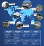
The rationale behind the Tower Semi acquisition and things to watch out for at Intel’s investor day.
Intel bids for Tower Semi
First I have to quote myself because Tower was an error of omission. In November in a piece that was likely too long for its own good, I mentioned that trailing edge fabs are in a huge position of strength… Read More
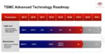
Recently, TSMC held their annual Technology Symposium, providing an update on the silicon process technology and packaging roadmap. This article will review the highlights of the silicon process developments and future release plans.
Subsequent articles will describe the packaging offerings and delve into technology … Read More
Summary
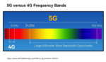
A recent process enhancement in advanced nodes is to support the fabrication of contacts directly on the active gate area of a device. At the recent VLSI 2020 Symposium, the critical advantages of this capability were highlighted, specifically in the context of the behavior of RF CMOS devices needed for 5G designs.
Introduction… Read More
On August 27, 2018, GLOBALFOUNDRIES (GF) announced that they were no longer going to compete in the race to the next smaller semiconductor node, at that time, the 7nm node. While surprising to some, on further analysis this move made sense. TSMC had announced its plan to invest around $25B in the 5nm technology node. GF revenue is … Read More
As analog and mixed-signal designers move to very advanced geometries, they must grapple with more and more complex considerations of the silicon. Not only do nanometer CMOS devices have limitations in terms of analog-relevant characteristics such gain and noise performance, but they also introduce new sources of variation… Read More