You are currently viewing SemiWiki as a guest which gives you limited access to the site. To view blog comments and experience other SemiWiki features you must be a registered member. Registration is fast, simple, and absolutely free so please,
join our community today!
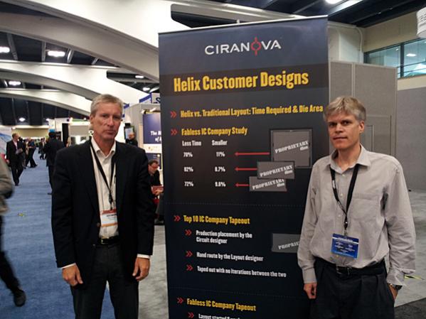
Three people from Ciranova met with me at DAC this year: Eric Filseth (CEO), David Millman (Marketing) and Lindor Hendrickson (CTO). They gave me an update on how the Helix tools are being used to automate the layout of custom IC designs at 28nm and smaller nodes.… Read More
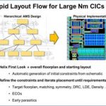
Ciranova presented a hierarchical custom layout flow used on several large advanced-node designs to reduce total layout time by about 50%. Ciranova itself does automated floorplanning and placement software with only limited routing; but since the first two constitute the majority of custom layout time, and strongly influence… Read More
On Tuesday, June 5th, starting at 3:05 pm in San Francisco, the planet Venus will cross, or transit, the sun. If you stop by Ciranova’s DAC booth #1608 anytime on Monday or Tuesday, they will give you a free pair of solar viewing glasses that will let you view the transit safely.
According to the NASA website, Transits of Venus… Read More
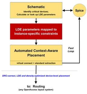
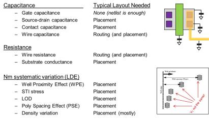
At 28nm and below, a number of electrical variation effects become significant which depend not only on individual devices, but the physical interaction between neighboring devices, wells, etc during the manufacturing process. Some of these effects have become collectively referred to as “Layout Dependent Effects” (LDE);… Read More
Recently I was researching the keynote speeches of isQED (International Society for Quality Electronic Design) Symposium 2012 and saw the very first, great presentation, “Taming the Challenges in Advanced Node Design” by Tom Beckley, Sr. VP at Cadence. I know Tom very well as I have worked with him and I admire his knowledge, authority… Read More
As analog and mixed-signal designers move to very advanced geometries, they must grapple with more and more complex considerations of the silicon. Not only do nanometer CMOS devices have limitations in terms of analog-relevant characteristics such gain and noise performance, but they also introduce new sources of variation… Read More
There are various rumors around about Cadence starting to close up stuff that has been open for a long time. Way back in the midst of time, as part of the acquisition of CCT, the Federal Trade Commission forced Cadence to open up LEF/DEF and allow interoperability of Cadence tools (actually only place and route) I believe for 10 years.… Read More
Verifying circuits on advanced process nodes has always been difficult, and it’s no easier with today’s nanometer CMOS processes. There’s a great paradox in nanometer circuit design and verification. Designers achieve their greatest differentiation when they implement analog, mixed-signal, RF and custom … Read More