VLSI’s business grew healthily but it never threw off enough cash to fund all the investment required for process technology development and capital investment for a next generation fab. They made a strategic partnership with Hitachi covering both 1um process technology and a significant investment, which meant that VLSI could build its second fab in San Antonio TX and had a competitive 1um process to run in it. At about the same time the San Jose fab was upgraded from 5” to 8” wafers.
The PC chipset business was very successful but it was clear that it would eventually become a low margin business due to competition from Asia, and probably would finally be owned by Intel who could design more and more functionality to work intimately with their own next-generation microprocessors. VLSI decided to invest in system knowledge for the GSM cellular standard that was starting to get off the ground, as well as some other attractive end markets such as digital video.
Also, in that era, Apple decided to build the Newton. They selected Acorn’s RISC processor and insisted it was spun out as a separate company. So ARM was created with Apple, Olivetti (that by then owned Acorn) and VLSI as the owners. VLSI’s expectations were that when the Newton took off that they would be building all the ARM silicon for Apple. This was still in an era where a 32 bit processor was a standalone chip. Of course, it turned out that the Newton didn’t take off and was canceled, and ARM had to create a new business model, licensing their processor cores to any semiconductor company that wanted it. Since only a few semiconductor companies had their own internal microprocessor development teams, this turned out to be a lot of companies. At the time, VLSI was not happy about having so many competitors in the ARM market, but once they discovered that they no longer had to convince customers that it was safe to use a microprocessor the customer had never heard of, that business grew strongly.
Meanwhile, market for second generation (digital) GSM phones exploded. European companies, especially Nokia and Ericsson, were the most successful handset manufacturers. At one point Ericsson was 40% of VLSI’s entire business. VLSI also built up a GSM chipset business selling to second tier manufacturers who didn’t have the system knowledge to develop GSM baseband chips internally.
In 1991 it was clear that VLSI was really two companies that should already have separated: an EDA company with some of the best VLSI design tools on the market, and an ASIC/ASSP company manufacturing silicon. So the design tool business was spun out as Compass Design Automation.
Compass struggled to shake off the perception that it wasn’t really independent of VLSI and as a result it had a relatively unattractive ecosystem of semiconductor companies that fully supported it with ASIC libraries. But Compass also had its own libraries, and by standardizing on the Passport design rules, which pretty much any fab could manufacture, it created a sizable library business of its own with standard cells, memory compilers and other foundation IP.
Compass grew to nearly $60M but it was never profitable. They had a fully integrated suite of design tools in an era when the large EDA companies, which had grown through acquisition, had educated the market to pick best-in-class point tools and use their internal CAD departments to do the integration. So Compass was swimming against the tide and despite the fact that every VLSI ASIC and every VLSI standard product was designed exclusively using Compass tools and libraries, they never shook off the perception that they were not leading edge and CAD groups were reluctant to standardize on Compass, at least partially because they would have nothing to justify their existence.
Eventually Compass was sold to Avant! who were mostly interested in the library business to complement their own software business. Of course, Avant! in turn was acquired by Synopsys. The software part of the business by then was largely based in France and the entire group in France was hired by Cadence en masse where many of the individual engineers still work today.
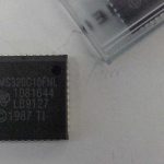
VLSI’s semiconductor business, both the ASIC business and the ASSP business grew to about $600M. There was a focus on wireless (not just GSM, VLSI had a CDMA license from Qualcomm too), digital video, PC graphics and an ASIC business that was diversified into many separate segments.
In 1999, Philips Semiconductors (now called NXP) made a hostile bid for VLSI Technology. Philips was a very bureaucratic company and struggled to bring processes to market quickly along with the required libraries. As the ASIC business got more and more consumer oriented, this became a big problem. VLSI’s lifeblood was ASIC and they were much quicker at getting designs going in new process generations, so Philips figured that acquiring VLSI would shake up their internal processes and also give them a network of leading design centers (by then renamed technology centers). After some back and forth negotiation, eventually VLSI was acquired by Philips Semiconductors for just under a billion dollars and it ceased to be an independent company.
VLSI’s Wikipedia page is here.