Semiwiki EDA Webinar 800x100

DFT Approaches for Giga-gate SoC Designs

DFT Approaches for Giga-gate SoC Designs
by Daniel Payne on 10-26-2016 at 12:00 pm

In the early days of IC design there were arguments against using any extra transistors or gates for testability purposes, because that would be adding extra silicon area which in turn would drive up the costs of the chip and product. Today we are older and wiser, realizing that there are product pricing benefits to quickly test each new SoC before packaging and even in the field. The biggest annual event in the test world has to be the International Test Conference (ITC), coming up November 15-17 in Fort Worth, Texas. I was able to speak with Ron Press of Mentor Graphics by phone about what they are doing at ITC this year. Here’s an overview:

  • Keynote by Wally Rhines, The Business of Test: Test and Semiconductor Economics (Tuesday, Nov 15, 9AM)
  • Tutorial 5, Diagnosis-driven Yield Analysis (Sunday, Nov 13, 1PM – 4:30PM)
  • Tutorial 9, Mixed-signal DFT and BIST: Trends, Principles and Solutions (Sunday, Nov 13, 1PM – 4:30PM)
  • Session 2.1, Test point Insertion in Hybrid Test Compression/LBIST (Tuesday, Nov 15, 2PM – 4PM)
  • Session 2.4, Minimal-Area Test Points for Deterministic Patterns
  • Session 17.1, Automated Measurement of Defect Tolerance in Mixed-Signal ICs (Thursday, Nov 17, 1:30PM – 3:30PM)

Full details of Mentor at ITC are online here. By the way, Ron is the General Chair for ITC 2016. The big three themes that I learned from Ron about testability this year were:

[LIST=1]

  • Giga-gate designs require hierarchical DFT approaches
  • Automotive test is growing and demanding
  • FinFET designs have unique diagnosis requirements

    Our present era has now enabled SoC designs with billions of gates, so how are you going to test that kind of a chip in a reasonable amount of time? The answer is to divide and conquer, applying the concept of hierarchical test to reduce ATPG run times, minimize RAM usage, and actually generate ATPG results much earlier in the design flow. This methodology lets test engineers create and validate patterns for each block, then automation enables reuse of the patterns as each block is placed in an SoC.

    Mentor also offers Embedded Deterministic Test (EDT) points that works with test compression to further reduce pattern volume giving you 2X to 4X additional compression on top of what their TestKompress approach offers.

    In the automotive world reliability of electronics is paramount, so they’ve created a standard called ISO 26262 and the EDA and semiconductor IP vendors have responded with both memory and logic BIST approaches. Field return analysis (RMA) is another key requirement for automotive. Mentor has created much of the test technology to meet the strict automotive requirements:

    The final of three major points is diagnosing faults in FinFET technology, where the challenge is to identify the root cause of a particular type of physical failure. The three letter acronym they use is called Root Cause Deconvolution (RCD) and this technique uses statistical enhancement to pinpoint failures starting from the logical diagnosis and ending up at the layout location:

    Transistor-level defects in FinFET designs can be located using cell-aware diagnosis for all of the pattern types (stuck-at, transition faults, cell-aware, etc.). The tools look at the FinFET layout and circuit schematic, then creates a cell-aware fault model specific to FinFET. Mentor has been using this sophisticated fault modeling since the 32nm node and smaller.

    If you attend ITC this year then consider checking out what the actual users of Mentor tools are talking about in their test experiences at the Posters: Samsung, Teradyne, Spreadtrum.


  • New Frontiers in the Storage System Market Call for the Best of ICE and Virtual Emulation

    New Frontiers in the Storage System Market Call for the Best of ICE and Virtual Emulation
    by Richard Pugh on 10-26-2016 at 7:00 am

    The storage market has reached what Andy Grove once described as “…a strategic inflection point.”[1] This is the stage in the life of a business when its fundamentals are about to change.

    Changing fundamentals in the storage market—where solid state drives (SSD) are now at the forefront of multiple storage applications, from enterprise-based datacenters to PCs—create both great opportunities and significant challenges. Both arise from new technical innovations, emerging standards, and the desire to reach higher performance, increase storage capacities, and meet the needs of system-level infrastructures—all at a lower cost per device.

    Delivering solutions for these challenges are where the Mentor Veloce® emulation platform demonstrates its strength as the hub of a sophisticated and comprehensive functional verification solution. One that gives design teams a catalyst to differentiate their enterprise storage devices that use SSD and NAND technologies.

    Emulation can verify the hundreds of millions of gates and multiple protocols now seen in SSD controllers along with the complex software that drives them. It has the speed to support full-chip hardware/software co-verification so that the RTL IP and software specific to a particular SSD controller can be verified together.

    Many protocols are still widely used in storage systems today (including SATA, SAS, PCIe, and NVMe). SSD device manufacturers need an emulation tool kit that offers solutions for them all. The Veloce emulation platform is without peer in this regard. Veloce provides in-circuit emulation (ICE) components (iSolve), virtual models (VirtuaLAB), and a unique new application (Veloce Deterministic ICE) to verify the design using the chosen host interface. Veloce also provides all the NAND, DDR, and NOR models used in conjunction with the SSD controller and software.

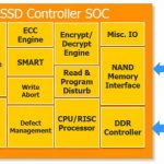
    Figure 1: SSD controller architecture.

    The Veloce iSolve library offers a full complement of hardware components to build a robust in-circuit emulation (ICE) flow, which is needed for many SoC verification scenarios.

    The Veloce Deterministic ICE App complements and extends the usability of an ICE-based environment by delivering a repeatable and virtual debug flow. In addition to offline SW debug, the Veloce Deterministic ICE App enables advanced debug capabilities, power analysis, and coverage closure methodologies.

    And the Veloce VirtuaLAB environment represents a new-generation of verification solutions delivering high-speed verification for multiple host protocols and memory devices, HW/SW system-level debug, power analysis, and system performance analysis.

    SSD on ICE
    When an SSD SoC design needs to be connected to real devices or custom hosts, the DUT (instantiated in the emulator) must be connected to physical hardware. In this case, teams use an emulation platform to set up the test environment by connecting the required peripherals/hosts using speed adapters/bridges to communicate with the SoC design mapped to emulator. Software teams make use of the ICE environment for firmware development and to run real applications. Verification teams use it to exercise various test methods to interact with the interfaces to verify the functionality of their SoC designs. Most designs today have an embedded CPU, and ICE is used for testing the OS boot cycles as well. ICE is also used for connecting proprietary hardware or proprietary operating systems (OS) to reproduce issues found in prototype or in a post-silicon lab setup.

    Making ICE Repeatable
    There are significant challenges in using ICE in certain scenarios, many of which are found in SSD verification. These include limitations on trace depth, long and iterative debug cycles, random and asynchronous events, and inflexibility in how the emulator can be deployed and shared. In addition, advanced verification techniques, such as power estimation, are not the best fit for a traditional ICE environment.

    The Veloce Deterministic ICE App addresses these challenges by creating a virtual debug model of an ICE run. Significantly, it adds determinism to the debug environment by making the test run repeatable cycle-by-cycle. It does this by generating a replay database to re-run or repeat the same test without the need for hooking up to ICE targets.

    Figure 2: ICE run.
    Figure 3: Using the replay database without ICE targets.

    While in replay mode, a user can choose to dump waveforms for an entire design for the duration of a test, or activate various other debug features (like live monitoring of important signals using streaming waveforms, enable displays, and protocol monitors), or do both. Having the ability to stop and inspect both data and full waveforms provides a rich debug platform and increased productivity in addition to efficient use of emulation resources.

    The Veloce Deterministic ICE App makes the test environment portable to other emulators or teams located in different places as the test is no longer dependent on the external ICE hardware. It also gives the flexibility to use other Veloce Apps like power analysis, SW debug, coverage, and assertions that would not have been feasible without this technology.

    The Virtual Lab
    Virtualization is the game changer for enterprise verification. Virtualization, which Mentor pioneered almost 10 years ago, allows emulators to be moved to centralized data centers to establish company-wide virtual platforms that support multiuser, software-driven SoC verification in a 24/7 enterprise server environment. Verification engineers can now access an emulator from their desktop, even from remote locations thousands of miles away from the emulator.

    Peripherals are virtualized via the Veloce VirtuaLAB environment. VirtuaLAB provides the same host interfaces as iSolve, including NVMe, but instead of using external hardware that must be cabled to the emulator, VirtuaLAB uses software protocol models. And, as VirtuaLAB uses the same IP as in ICE solutions, so it delivers the same functionality as iSolve hardware peripherals.

    Importantly, VirtuaLAB delivers emulation performance equivalent to that of ICE, making it an attractive alternative that is better suited to multiple users and applications.

    VirtuaLAB allows an SSD controller designer to run and debug the same software applications in the VirtuaLAB environment as they would on the real hardware. VirtuaLAB also eliminates the need for hardware speed adapters/bridges, and supports third-party performance analysis and power analysis applications. This means designers can do all of the same statistics, analysis, and metrics that they would do on the real design, but it’s done pre-silicon.

    The Best of Both Worlds
    With the Veloce emulation platform, verification teams have access to the best of both worlds—ICE and virtual emulation—powered by the world’s most versatile and flexible emulation technology.

    The Veloce emulation platform is radically recasting the emulation landscape, making emulation friendlier and more useful, while delivering all of the speed, visibility, and performance of traditional ICE-based emulation. The Veloce emulation platform is uniquely built with highly scalable hardware, an extensible operating system, proven virtual solutions, and a growing library of apps that solve application-specific verification challenges.

    To learn more about the rise of SSD technology and Mentor’s emulation solutions for storage system designs, check out the new whitepapers Veloce Delivers Best of ICE and Virtual Emulation to the SSD Storage Market and Using the Veloce Deterministic ICE App for Advanced SoC Debug.

    [1]Only the Paranoid Survive, Andy Grove, Crown Publishing Group, May 5, 2010


    2016 semiconductor capex highest in 5 years

    2016 semiconductor capex highest in 5 years
    by Bill Jewell on 10-25-2016 at 4:00 pm

    Global semiconductor capital expenditures (capex) are expected to return to the level of 2011 either this year or next. 2011 was the record year for capex as the industry returned to growth following the 2009-2010 recession. IC Insights’ August 2016 forecast called for 3.5% growth in capital spending to reach $67.1 billion, the highest level since $67.4 billion in 2011. Gartner’s October 2016 projection was a slight 0.3% downturn in 2016 followed by 7.4% growth in 2017 to reach $69.3 billion, surpassing $65.8 billion in 2011.

    Semiconductor manufacturing equipment accounts for about half of semiconductor capital spending. In August 2016, SEMI called for 4.1% growth in equipment in 2016, accelerating to 10.6% in 2017. Gartner’s October forecast has fab equipment growing in the 6% to 7% range in both 2016 and 2017. Neither SEMI nor Gartner has 2017 equipment returning to the 2011 levels of $44 billion to $45 billion.

    Solid growth in semiconductor fab equipment in 2016 is supported by data from SEMI and the Semiconductor Equipment Association of Japan (SEAJ). Combined SEMI and SEAJ data shows 3[SUP]rd[/SUP] quarter 2016 semiconductor manufacturing equipment billings were $8.5 billion, up 7% from the prior quarter and up 12% from a year ago. Bookings were $8.6 billion up 27% from a year ago but down 2% from the prior quarter. The resulting book-to-bill ratio was 1.02. We at Semiconductor Intelligence are projecting full year 2016 equipment billings will be up 12% from 2015. The slowing in bookings could be indicating billings are close to a peak. However even if billings remain at the 3[SUP]rd[/SUP] quarter 2016 level through the end of 2017, 2017 growth would be around 8%.

    Which companies are driving semiconductor capital spending? For several years, capex has been dominated by microprocessor giant Intel, the largest memory company Samsung, and the major wafer foundry TSMC. These three companies have accounted for 44% to 56% of total capex for each of the last five years. The table below shows the largest companies in capital spending based on 2016 projections. Most of the 2016 numbers are based on company guidance. IC Insights estimates were used for Samsung, GlobalFoundries and total capex.

    Samsung should have the largest capex in 2016 at $11.0 billion, according to IC Insights. Samsung has had the largest capex for several years. Intel and TSMC are each projecting 2016 capex of about $9.5 billion. The four largest memory companies account for 37% of capex. Besides Samsung, Micron Technology capex is $5.4 billion (based on fiscal 2016 ended September 1) and SK Hynix projects $5.2 million. Micron should pass SK Hynix to become the second largest memory company in capex for the first time. Flash Ventures, a joint venture flash memory company between Toshiba and SanDisk (now part of Western Digital) should spend $3.5 billion.

    The four largest foundry companies total 26% of projected 2016 capex. After TSMC, the next largest companies are GlobalFoundries at $3.0 billion, SMIC at $2.5 billion and UMC at $2.2 billion in capex. GlobalFoundries has lowered capex each of the last two years after peaking at $5.0 billion in 2014. China-based SMIC has been aggressively increasing capex averaging 50% annual growth over the last four years to hit $2.5 billion in 2016.

    Other companies make up 23% of projected 2016 capex. This category includes major semiconductor companies such as Infineon Technologies, NXP Semiconductor (now including Freescale), Renesas Electronics, STMicroelectronics and Texas Instruments. As new wafer fabs have become more expensive (now costing several billion dollars) these companies are depending less on internal fabs and increasingly turning to foundries. Intel is an exception since it has a large economy of scale and sees its process technology as a competitive advantage. The memory companies also have economies of scale. In addition, the memory market is highly commoditized and price sensitive, making it difficult for a company to compete without its own wafer fabs.

    The “other” category has been declining as a percentage of total semiconductor capex, from 39% in 2010 to 23% in 2016. The category will continue to decline in the future as capex is increasingly dominated by memory companies, foundry companies and Intel.


    End-to-End Secure IoT Solutions from ARM

    End-to-End Secure IoT Solutions from ARM
    by Bernard Murphy on 10-25-2016 at 11:30 am

    ARM announced today a comprehensive suite of solutions for IoT support, from IP optimized for applications in this space all the way to cloud-based support to manage edge devices in the field. Their motivation is to provide a faster path to secure IoT, from the chip to the cloud. One especially interesting component of this solution is a cloud-based software-as-a-service (SaaS) to manage, provision and update edge devices through a common platform. Simply put, ARM’s offering is about how little you now have to build or integrate yourself to get an end-to-end secure IoT solution up and running.

    Before we go to the cloud, let’s start with what ARM is doing for edge nodes. First, they have introduced two new microcontroller cores: Cortex-M33 and Cortex-M23. These cores build on the ARMv8-M architecture and are the first in the Cortex-M family with TrustZone built-in. The M33 provides a lot of flexibility, with DSP and FPU on board and with a co-processor interface, yet is 80% smaller than the Cortex-A5. ARM anticipates that this platform will become the mainstream MPU for secure embedded. The M23 is 75% smaller still and 50% more energy efficient. To give an idea how low power this can be, think about pulling an insulin pen out of a holder. Sufficient kinetic energy can be harvested from this action to support battery-free operation.

    TrustZone architecture, now available in these new M-class cores, provides similar capabilities to those available in other families. A Corelink SIE-200 fabric connects the processor to peripherals, mediating secure-world versus normal-world access under control of the processor which itself transparently time-slices between the two worlds with no need for programmer intervention. You get secure operation without needing an extra security CPU.

    Cryptocell-312 adds the security resources required to build a trusted execution environment (TEE), through faster and lower-power cryptography performance. It also offers symmetric and asymmetric ciphers, hashing and random number generation, lifecycle management and root-of-trust controls, along with many more features. And it’s configurable so you can dial area and power down to address just what you need in your solution.

    Another very important aspect supported in this series is secure debug. Cryptocell allows you to define and control a debug policy allowing differing levels of debug access in manufacturing, to the OEM and (per OEM grants) to field-deployment and maintenance teams.

    Then there’s the Cordio radio. The latest release supports both Bluetooth 5 and 802.15.4 for ZigBee and Thread, covering the most popular choices for IoT. You can get the radio as a hard macro in TSMC 40LP/ULP or 55LP/ULP processes or in UMC 55ULP, or you can use the link-layer controller RTL and stack with a 3[SUP]rd[/SUP]-party radio front-end and process of your choosing. You can also have both Bluetooth and 802.15.4 in one Cordio-C50 macro with a modest increase in area and you can dynamically switch between modes. ARM mentioned that it was also feasible to operate Cordio on harvested energy, where appropriate.

    ARM also offers all of this together in the pre-packaged Corelink SSE-200 subsystem: an ARMv8-M core, CryptoCell 312, the Cordio radio, memories and peripherals, all tied together with the CoreLink fabric and built on top of the Artisan IoT physical IP optimized to a low-power IoT use-model and targeted to the TSMC 40nm ultra-low-power process. That subsystem gets you a fast, low-power, secure and low-risk solution ready-made, allowing you to focus on adding your own special sauce.

    Which brings me finally to mbed Cloud. A high security edge device isn’t very useful unless you also secure cloud-based management of those devices. Now think about trying to integrate a mix and match solution between multiple providers of devices and cloud access. I have a hard time imagining how you could avoid deploying a solution with security holes and power-wasting communication bugs. Third-party applications still have a role, but sitting on top of a secure, low-power foundation managed by one provider. ARM’s extension to provide the cloud part of this foundation through a SaaS solution is a new departure of course, but it seems to me unavoidable given security demands.


    mbed Cloud has four major objectives: to be multi-cloud capable, to cover any device (not just ARM-based systems), to be very energy-efficient in management of devices and to secure every transaction. ARM acknowledge they are going to have to fold into legacy networks – devices, OSes, gateways and more, so the management solution has to span all of these. For connectivity mbed Cloud will communicate through CoAP, also OMA LWM2M, for provisioning it will take care of injecting security assets into a device and will manage access rights through the device lifecycle. And it provides fail-safe and secure update through broadcast and mesh-friendly packages.

    Together with Mbed OS 5.2, mbed Cloud 1.0 has been announced at ARM TechCon 2016. The solution is already open to a number of lead partners in smart factory, industrial IoT, asset tracking and healthcare applications. ARM expects the release to be more broadly available in Q1 of 2017. The business model for cloud support apparently will be similar to other SaaS models – an OEM subscribes to just the features they use. You can learn more about ARM IoT solutions HERE.

    More articles by Bernard…


    Emergence of Segment-Specific DDRn Memory Controller

    Emergence of Segment-Specific DDRn Memory Controller
    by Eric Esteve on 10-25-2016 at 7:00 am

    The semiconductor industry is served today by memory devices supporting various protocols, like DDR4, DDR3, LPDDR4, LPDDR3, GDDR5, HBM, HMC, etc. The trend is clearly to define application specific memory-protocols and in some cases, application specific devices. But developing many, and different, memory controllers IPs is resource and time consuming and not the best option for a vendor. For the chip-maker developing the System-on-Chip (SoC), the goal is to select memory protocol allowing integrating cost optimized memory devices, offering the best performance to cost ratio. If we look at the various, above listed, protocols, the DDR3 (DDR4) and LPDDR3 (LPDDR4) devices are offering by far the best cost/performance compromise. The DDRn or LPDDRn protocols support a wide range of applications, from low power mobile application processor to high performance, high bandwidth infrastructure application, like servers, storage or networking.

    The question is how to define a unique memory controller which could be optimized to best support various applications like high-end consumer, mobile and infrastructure through parameterization. The memory controller IP is the most crucial piece of design in a SoC. If this IP fails, the SoC is simply not usable. That’s why the SoC chipmaker will take advantage of a unique memory controller design that is more robust, stable and easier to maintain by the IP vendor than a variety of hard macros. This paper summarizes a white paper from Cadence “Emergence of Segment-Specific DDRn Memory Controller IP Solution” and the technical data are related to Cadence’ memory controller IP products developed in 28 nm and 16 nm.

    SoCs developed for networking applications requires the delivery of high bandwidth while running high performance computing and achieving large memory capacity. High bandwidth, along with large memory capacity and performance requirements, are expected to be directly translated to the memory controller IP and expected to deliver more data per cycle at the highest possible frequency. SoC targeting infrastructure segments have to provide a rich set of enterprise-class RAS (reliability, availability, and serviceability) features.

    The protocols supported reduce to DDR3, DDR3L, and DDR4, as there is no need for LPDDRn support. The maximum data rate is 3200Mbps (note that overclocking is not supported in order to keep maximum data integrity and not impact the reliability). The data bus is set to 72 bits by default (it can be 16, 32, 40, 64 or 72 bits wide), and the address bus is set to 18 bits by default, allowing the user to access the largest possible memory space. Several features have been specified to best fit with the requirements of infrastructure applications, like DQ-to-DQS ratio (set to 4:1 compared to 8:1 in the other two configurations) to minimize the maximum skew between clock (DQS) and data (DQ). The memory controller supports per-rank-leveling (PRL) as well as write leveling for x4 DRAM to maximize data integrity, the goal being to optimize system reliability.

    In the infrastructure segments, the CPU must use as much memory space as possible, and using dual inline memory modules (DIMM) is a must-have feature. The Cadence memory controller IP solution supports registered DIMM (RDIMM), unregistered DIMM (UDIMM) and load reduced DIMM (LRDIMM). In fact, these DIMM configurations are not supported in the other segments, the feature is infrastructure specific.

    The white paper will tell you about the other two set of configuration features, defined for the mobile segment and for high-end consumer applications. Developing 100% application specific IP would be an ideal solution, but not realistic. Based on a unique architecture, this memory controller IP is highly configurable, this configurability allowing supporting the requirements of applications as different as servers/storage, mobile application processors or high-end consumer.

    The white paper “Emergence of Segment-Specific DDRn Memory Controller IP Solution” is available on Cadence web site: http://ip.cadence.com/uploads/1102/wp-dip-ipnest-ddr-for-apps-final-pdf

    By Eric Esteve from IPNEST


    FPGAs for a few thousand devices more

    FPGAs for a few thousand devices more
    by Don Dingee on 10-24-2016 at 4:00 pm

    An incredibly pervasive trend at last year’s ARM TechCon was the IoT, and I expect this year to bring even more of the same, but with a twist. Where last year was mostly focused on ultra-low power edge devices and the mbed ecosystem, this year is likely to show a better balance of ideas across all three IoT tiers. I also expect a slew of ADAS applications to hit the show.

    The two IoT tiers besides the edge – gateway, and infrastructure – have room for bigger, more capable chips with either power-over-Ethernet, or wall power available. ADAS applications have vehicle power to work with, and while they have thermal restrictions limiting power dissipation, we’re also seeing larger chips to handle tasks like embedded vision, radar, and lidar.

    Every time I bring up “IoT” and “FPGA” in the same sentence, people pounce. I get it, though my first response is the IoT does not equal edge sensors and actuators and mobile devices. FPGAs don’t fit the power profile of most edge devices, but with fog computing taking on a larger role things are starting to change.

    Economically, we have the “a billion is the new million” problem, and the lower volume applications don’t make sense for custom silicon starts. Somebody still has to take care of those applications needing a few thousand devices. In the past, that was often a merchant microprocessor on a COTS single board computer with daughtercard mezzanines to customize I/O requirements.

    We’ve also talked a lot about optimization making sense for IoT chip starts, and most FPGA designs don’t seem optimized versus an ASIC solution. Yet, these applications are ripe for solutions such as Xilinx Zynq, combining the benefits of dual core processing with programmable logic. For decades, FPGAs have succeeded at relatively low volume, heavily customized applications such as broadcast video solutions and defense signal processing. Industrial IoT solutions call for low to mid-range volumes in the gateway and infrastructure tiers.

    Optimization is an interesting discussion. It gets really hard to optimize things when what you really need is flexibility. With specifications moving around, consortia merging, and market forces still not indicating a clear winner for industrial IoT solutions, FPGAs present an opportunity. Designs can be completed in programmable, accelerated hardware, fielded, and changed quickly to respond to the next customer requirement.

    ADAS is a bit more complicated, because there are millions of cars out there and the volumes are attracting merchant chip starts. However, we are seeing the same fragmentation – he who owns the algorithms and the maps will ultimately win. Committing to a strategy, be it GPUs, CNNs, DSPs, or hardware-accelerated instructions, is expensive. It might win a particular customer and completely miss the wants of another. There are questions of differentiation and ecosystems and who is willing to make joint investment instead of demanding NRE.

    Experimentation is rife in ADAS space. In a lot of ways, the algorithm scientists own the problem right now. This is almost the case for what John Bruggeman tried to pitch several years ago, where the silicon would self-organize around the software. We’re a long way from ASICs doing that, but development tools such as Xilinx SDSoC taking algorithms directly from C/C++ to FPGA hardware can approximate at least the compute intensive part of the solution.


    One of the first press releases to cross my desk for this year’s ARM TechCon is from Aldec, parlaying Zynq technology into both ADAS and IoT applications. They are demonstrating two embedded development kits (EDKs) based on their TySOM family:

    • Their ADAS setup has their TySOM2 module plus an FMC with four camera interfaces streaming four First Sensor Blue Eagle cameras, complete with edge detection, colorspace conversion, and frame merging in programmable logic.
    • For IoT gateway applications, the TySOM1 is showing off MQTT and Amazon Web Services (AWS) integration with sensors of various protocols connected to the gateway. Aldec has been working with hardware-accelerated encryption for this platform, as well as adding more sophisticated vision sensors.

    Also in booth #215, Aldec will be showing co-emulation using ARM Cortex-A15 fast models running SCE-MI. More on the Aldec presence at ARM TechCon:

    Aldec to Showcase Xilinx Zynq-based ADAS and IoT Gateway Development Platforms at ARM TechCon 2016

    Maker modules took the IoT world by storm because they are only twiddling a few bits with an MCU or dealing with a couple standard I/O ports off a mobile SoC. For the next wave of industrial IoT and ADAS applications, where customization and hardware acceleration of code are differentiators, Aldec and other Zynq-based module suppliers have a better formula.


    Making your AMS Simulators Faster (webinar)

    Making your AMS Simulators Faster (webinar)
    by Daniel Payne on 10-24-2016 at 12:00 pm

    I’ve been following Cadence Design Systems ever since it was formed in 1988 by the merger of SDA Systems and ECAD, Inc. At that time I was working at Silicon Compiler Systems, soon to be acquired by Mentor Graphics. ClioSoft is another company that I’ve known about for several years now, mostly for their design management tools that work inside of popular EDA environments like the Cadence Virtuoso system used by AMS designers.

    Related blog – 3 small-tem design productivity challenges managed

    Some of the challenges with AMS designs for IC teams today is that design engineers can be spread across multiple sites, even in different time zones or in different countries. With a time to market deadline looming, it can be difficult to properly communicate with all of the designers about which version of every IP block to be using on their project, when there can be hundreds of different blocks. Fortunately for us these two EDA vendors – Cadence and ClioSoft, have been working together on integrating design management into the Virtuoso environment.

    Related blog – Organizing data is first step in managing AMS designs

    There’s a webinar on Wednesday, October 26th at 10:30AM PST that you will want to attend if you use any of the Cadence tools, like:

    • Virtuoso ADE Explorer
    • Virtuoso ADE Assembler
    • Virtuoso Variation Option
    • Virtuoso ADE Verifier
    • Maestro View

    Related blog – 10 challenges in IP design collaboration

    Steve Lewis from Cadence will be talking about their analog design suite and how Virtuoso IC6.1.7 works in an IC design flow. Next up in the webinar is Karim Khalfan from ClioSoft to demonstrate how their SOS7 design management tools work inside of the Cadence Virtuoso environment. You’ll also get to see how Maestro View works and how the IC6.1.7 release has gotten quicker to use.

    Register for the Webinar today.

    The SOS software from ClioSoft is used for both design and semiconductor IP management by hardware designers on an IC team. It’s kind of unique because it spans digital, analog, RF and mixed-signal designs. Your design teams can be in a single or even multiple design centers, then collaborate using automation on their projects.

    About ClioSoft
    ClioSoft was launched in 1997 as a self-funded company, with the SOS design collaboration platform as its first product. The objective was to help manage front end flows for SoC designs. The SOS platform was later extended to incorporate analog and mixed-signal design flows wherever Cadence Virtuoso[SUP]®[/SUP] was predominantly used. SOS is currently integrated with tools from Cadence[SUP]®[/SUP], Synopsys[SUP]®[/SUP], Mentor Graphics[SUP]®[/SUP] and Keysight Technologies[SUP]®[/SUP]. ClioSoft also provides an enterprise IP management platform for design companies to easily create, publish and reuse their design IPs.

    Also Read

    3 small-team design productivity challenges managed

    Organizing data is first step in managing AMS designs

    Webinar alert – helping mixed signal not be mixed up


    CEO Interview: Simon Butler of Methodics

    CEO Interview: Simon Butler of Methodics
    by Daniel Nenni on 10-24-2016 at 7:00 am

    It has been interesting to watch Methodics transform from an EDA company with their VersIC design management product to Life Cycle Management with ProjectIC, and now a Systems Company with WarpStor. Methodics was founded in 2006 by 2 ex-Cadence experts in the Custom IC design tools space, Simon Butler and Fergus Slorach. Today Methodics delivers state-of-the-art IP Lifecycle Management, Design Data Management, and Storage and Workspace optimization and acceleration tools for analog, digital, SoC, and software development design teams.

    The term “IP” gets tossed around a lot, but it seems to mean different things to different people. How do your customers view the term “IP” and do you see the definition converging to any particular class?
    “IP” and design re-use are closely related. Companies realize that the only way to meet new time to market demands and cost constraints is to be able to either reuse as much design as possible from previous designs, or purchase “IP” from third parties to meet these goals. Therefore, IP takes many different definitions depending on where it is coming from. It can be design data, software code, PDK’s, configuration files, documentation, hierarchical “blocks of blocks”, almost anything related to the design process. This is what the challenge is.. how can this disparate data be managed?

    As companies adopt strategies that help them reuse their existing IP alongside 3rd party IP, are you seeing other methodologies that can help even further?
    The biggest challenge is once you decide to re-use IP, you still have a configuration and connectivity issue. These IP blocks must work together. The problem is how to not lose the benefit of not having to redesign everything, only to spend the same time integrating the IP blocks. Companies are now starting to look towards “Platform Based Design” strategies, where IP is integrated before a new design starts into a platform that already works. To make this work, IP’s are designed to be plug and play into a common platform prior to be targeted towards a new design. Therefore, design teams are not downloading individual blocks that they must make work together, but a known good starting point of a functioning platform and can concentrate on any customization or new code development for the final design. This also simplifies product families within companies, because products are naturally grouped by the commonalities of IP used.

    What challenges do you see companies need to overcome to realize these IP reuse and platform based design methodologies?
    First, there has to be a change in mindset on what IP is… that “designing for re-use” is not a heavyweight methodology shift requiring additional work from designers to make happen. Configuration information, meta data, and related design artifacts need to be able to be easily maintained in order to facilitate adoption.

    Also, the notion that there needs to be a major methodology change to make this happen needs to be dispelled. A system for facilitating IP reuse needs to be easy to integrate into existing design flows with little to no overhead.

    With all the consolidation that is happening in the Semiconductor Industry, what impact do you see on the need to adopt IP reuse methodologies?
    These mergers are being driven so that companies can maintain a healthy and competitive business. With companies merging to increase product portfolios, or to move to a more complete solution for their customers, they must create efficiencies in the product design flows. If a company doubles it product portfolio, or vertically integrates designs to provide a more complete system, you cannot lose business optimizations to a decrease in design productivity. Companies must be able to leverage all IP within the new organization in order to maintain efficiencies that were brought about by the merger. It is business critical to make sure the infrastructure is in place to facilitate design reuse throughout the new, post-merger organization.

    What do you see as a requirement within companies to be able to effectively adopt IP re-use methodologies?
    Companies need a collaborative platform that tracks the IP being created in the system, and how those same IP’s are being used by designers in multiple projects. There should be no differentiation between design data and IP, because any design artifact can be IP in another design. You should not limit your IP catalog to some static, manually maintained catalog determined by some librarian or IT person that does not have visibility into all designs, but allow designers to search all designs for possible IP and re-use candidates.

    There are many solutions out there for semiconductor design data management and IP management, what makes Methodics unique?
    Methodics has a system of collaboration that connects IP consumers to IP creators. It tracks the IP lifecycle in a project context that can be summarized in easily configured dashboards with all access to IP meta data. Any interested party has access to what IP is available, its state and quality, and how and where it’s used in other projects. Importantly, Methodics does not differentiate between design data and IP data – it is all treated the same and can be made accessible to anyone at anytime based on access policies and permissions. The IP management platform is lightweight and can be seamlessly integrated in design environments. With IP management in place, design decisions are more historically informed and contextually aware. Instead of being seen as a mandate that comes with a lot of overhead, “IP management” is a process that happens in the background and then becomes a guide to making better design decisions.

    Also read: 

    CEO Interview: Charlie Janac of Arteris

    CEO Interview: Marie Semeria of LETI

    CEO Interview: Geoff Tate of Flex Logix


    Foundry is Majority of KLAC Business!

    Foundry is Majority of KLAC Business!
    by Robert Maire on 10-23-2016 at 8:00 pm

    As we had projected, with KLA having the highest exposure to foundry/logic of any tool company, they are seeing the most near term strength as foundries (read that as TSMC) spend big for 10NM and 7NM. In addition the first tools you buy are yield management/metrology tools which KLA is the king of.

    KLA put up numbers well above estimates….Generating $751M in revenue versus expected $733M and EPS of $1.16 versus street of $1.03. More importantly next quarter revenue is expected to be between $805M-$865M and EPS is expected to be between $1.28 and $1.48 this is way above street estimates of $770M and $1.19 in EPS

    Is this to end or just begin? – Led Zep
    We think KLA is at the beginning of a long run of strong demand to support both the 10NM and 7NM nodes. Industry expectations of 7NM being a “big” node like 28NM means a lot of equipment will need to be bought. Meanwhile 28NM capacity continues to be added. Unlike other tool companies where there seems to be investor concern about the sustainability of the current spending cycle, we think KLA is at the beginning …

    Both Gen4 and Gen5…

    KLA is seeing strong interest in both revamped versions of its Gen4 tools as well as its latest and greatest Gen5 tools. KLA is also seeing broad demand across its different product segments. We see no new significant competition in its core markets, and the company maintains its very strong market share as well as high gross margin that goes with that dominance

    2017 could be a good year for KLA…
    Given the strong start to the fiscal year coupled with good product positioning & mix as well as better foundry/logic demand we think KLA could be back on track to the strong performance it previously enjoyed before memory became so dominant in the market. While its clear that 3D NAND spend is still going strong we think the balance with foundry/logic will be more normal going forward and that helps KLA

    The stock…
    If we were to guess about a potential $6 EPS number for fiscal 2017 and then applied KLA’s historical 15X PE multiple to it , we get a $90 stock valuation which we think is well within a conservative range given KLA’s superior financial model and market dominance.

    This obviously implies large potential upside in the stock, getting a nice dividend in the meantime doesn’t hurt either and likely limits the downside.

    The KLA story has been hidden beneath the covers of the KLAM deal for the last year and we think as large, long only funds rediscover the name, we will likely continue to see strong steady improvement in the stock.

    About Semiconductor Advisors
    Semiconductor Advisors provides this subscription based research newsletter, Semiwatch, about the semiconductor and semiconductor equipment industries. We also provide custom research and expert consulting services for both investors and industry participants on a wide range of topics from financial to technology and tactical to strategic projects.


    Foundry CAPEX Jumped from 17% to 37% of LAM Business

    Foundry CAPEX Jumped from 17% to 37% of LAM Business
    by Robert Maire on 10-23-2016 at 4:00 pm

    Lam- in line qtr but guides above street over near term. As with ASML, foundry is driver with subdued memory, The Math implies biz peaking-Looking for DRAM in 2017.

    Lam reported another great, record quarter, more or less in line with expectations with revenues coming in at $1.632B and shipments of $1.708B, generating EPS of $1.81. As we had previously predicted, forward guidance was off the charts with the December quarter revenues expected to be $1.84B +- $75M and shipments to be $1.85B +- $75M, generating $2.18 in EPS.

    The company paid back some debt that was earmarked for the KLAM deal and will likely restart and potentially increase buybacks and/or increase dividends with some leftover cash. Foundry jumped from 17% to 37% of business, with memory down and logic flattish. The subdued memory likely limited upside in the just reported quarter and Samsung was likely slower than previous memory spend.

    TSMC terrific….
    Foundry spending was the big driver with 10NM/7NM being at the core and we are sure TSMC, the biggest foundry, is prepping to produce parts for Apple’s next Iphone next year. While foundry spending was up 25%, Lam said its foundry business was up 40% suggesting significant share gains and SAM expansion.

    2017 will depend a lot on DRAM….

    With 3D NAND and foundry continuing their strong pace the missing link is DRAM which saw a drop of 40% in spending this year. The most significant variable in spending outlook in 2017 is wether or not DRAM comes back. So far the signs look promising as pricing is good but we still wouldn’t count our chickens before they are hatched.

    A new beginning (in New York)

    Lam pushed back its analyst meeting , which was originally intended to be a KLAM celebration, back by two days and East by 2500 miles to New York. Much as Applied did after the failed TEL merger, we heard the new business model and targets set forth. We expect both a reset on the Lam business model as well as renewed returns to shareholders either through buy backs or dividends.

    One issue we have is that its a bit of short time period to come up with a new plan and business model in 5 or 6 short short weeks after the end of the KLAM deal when planning for the KLAM deal went on for almost a year. We expect the real recovery to be more like 6 months or more to get fully back on track, much as we saw at Applied. But at least we will get an idea of the new strategic direction.

    Running the numbers…
    When we do the math on the guidance for the December quarter versus Lam’s expectations for the overall capex market next year it seems clear that the rate of growth will either slow or reverse. Much of the math is dependent on the state of DRAM and its recovery. Lam’s SAM has expanded greatly but we would likely to hear where the new SAM is coming from now without KLA, ….hopefully at the analyst meeting.

    As we had previously predicted the next few quarters will be strong but investors will want to understand the longer term as fear increases that we are nearing a top because in previous cycles we saw a similar spurt of growth before a downturn started.

    Predicting KLAC ….

    If foundries were good for Lam, they will be fantastic for KLAC as they get a much bigger benefit from foundry/logic spending trends we are currently seeing. The reports out of both ASML and Lam confirm the current foundry ramp.

    The stock…

    Given the December guidance of $2.18 EPS, we are looking at a potential of a $9+ in EPS in 2017 , even if we flat line earnings. $9 in earnings is likely worth $110 a share or better but investors need to be comfortable that growth will continue and not top out or fall off in 2017 after several strong quarters. We are sure management will make the case at the analyst meeting….so far the track record has been good…

    About Semiconductor Advisors
    Semiconductor Advisors provides this subscription based research newsletter, Semiwatch, about the semiconductor and semiconductor equipment industries. We also provide custom research and expert consulting services for both investors and industry participants on a wide range of topics from financial to technology and tactical to strategic projects.