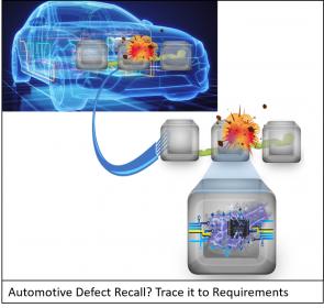
Next week is ARM TechCon which is one of my favorite conferences (SemiWiki is an event partner). This year is lucky number thirteen for ARM TechCon and it includes more than sixty hours of sessions plus more than one hundred ARM partners in the exposition. I will be signing free copies of our new book “Custom SoCs for IoT: Simplified” in the Open-Silicon booth #918. Please stop by Wednesday morning and get a book. It would be a pleasure to meet you!
This year Mentor Graphics, A Siemens Business, is a platinum sponsor and has an impressive line-up. Emulation of course is featured due to the conference emphasis on silicon design to software development. Emulation is a fast growing market and, coincidentally, is the topic of our next book (a collaboration with Mentor) which is due out early next year:
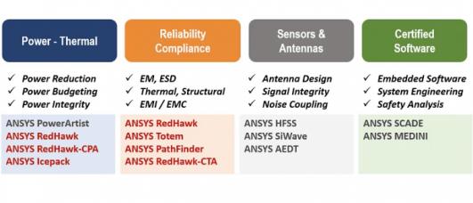
Mentor Graphics delivers the most comprehensive Enterprise Verification Platform™ available for ARM based SoCs and Interfaces: including the Visualizer™ Debug Environment for common debug across simulation, formal, emulation and prototyping, Questa® for high performance simulation, verification management and coverage closure, low-power verification with UPF, CDC, Formal Verification and Veloce® for high-performance system emulation, hardware/software co-verification or integration, system-level prototyping, and power estimation and performance characterization. This comprehensive platform supports UVM. Come check out our latest demos…
Tanner EDA is also featured this year which makes complete sense considering their focus on AMS and MEMs design. I worked with Tanner prior to the acquisition and am a big fan of their tools. I pushed for the acquisition believing that Mentor and Tanner would be a 1+1=3 proposition and I was right, absolutely.
Tanner EDA offers complete design flows for the design, implementation and verification of Analog, Mixed Signal and RF integrated circuits, as well as MEMS. Tanner enables the next generation of IoT edge devices by making it easier for to designers of sensors, MEMS and actuators to create custom SoCs…
Low power design has also been a top trending key word on SemiWiki as it touches just about every market segment and I do not expect that to change ever. Low power design is also prevalent at Arm events for obvious reasons which is why Catapult is also featured:
The Catapult® High Level Synthesis (HLS) PowerPro® Register Transfer Level (RTL) Lower-Power family of products enable ASIC, SOC and FPGA designers to quickly create fully-verified, power-optimized RTL for downstream synthesis and physical design…
And of course Mentor Embedded is featured due to the more than four thousand embedded designers that are expected to attend:
Mentor solutions for Arm® processors enable the development of advanced embedded systems, scalable footprint for Cortex®-M and Cortex®-A applications targeting single to heterogeneous multicore devices for high-performance, power-efficient, secure and safety certified embedded devices. Embedded developers can create systems with the latest Arm processors and micro-controllers with commercially supported and customizable Linux®-based solutions including the industry-leading Sourcery™ CodeBench and Mentor® Embedded Linux products. For real-time systems, developers can take advantage of the small-foot-print and low-power-capable Nucleus® real-time operating system (RTOS)…
See the full Mentor ARM TechCon landing pageHERE
See the ARM TechCon WebsiteHERE
See SemiWiki ARM contentHERE
See SemiWiki Mentor ContentHERE