 Mentor, A Siemens Business, just released a new white paper entitled, “The True Costs of Process Node Migration” written by John Ferguson. This is a good quick read that highlights some of the key areas that are often over looked when contemplating a shift of process nodes for your next design.
When considering a shift to a more advanced node we normally think of cost reductions brought on by smaller transistor sizes and pitches. The smaller the transistors and the tighter the pitch, the more logic you can fit on a die, essentially reducing the cost per transistor.
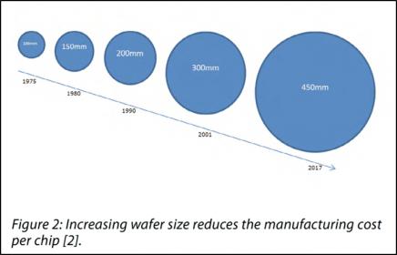 Over time, foundries further ingrained this idea by compounding savings through shifts to larger wafer sizes, again usually associated with new process nodes. Wafer sizes have grown from 100mm in 1975 to 450mm presently being used in state-of-the-art processes. The bigger the wafer, the more die that can be produced for the cost of that wafer. While prices for 450mm wafers are considerably higher than their 100mm counterparts, the number of die that can be processed on a wafer goes up as a function of the available area (e.g. square function) and the aggregate costs per die come down. That’s the good news.
John’s white paper goes on to expose many of the hidden costs that people often forget to consider. One hidden cost is that if the die size stays constant and the logic size increases, it follows that more interconnect will be required to connect the logic. This comes at the price of additional metallization layers which adds to both the wafer processing costs and non-recurring engineering (NRE) costs for the extra metallization masks. Additional metallization implies additional chip power to push the signals through the extra layers and vias. More power can also mean a more expensive package to handle the extra heat generated.
Another hidden cost comes from the fact that the geometric pitch on advanced nodes really hasn’t decreased much since the transition to nodes requiring multi-patterning lithography (e.g. 20nm and below). The good news here is that the transistor pitches are still shrinking as we’ve turned the transistor on its proverbial side using FinFET technology. However, the wafer processing and mask NRE costs to perform these miracles are rising at a much higher rate than previously, so the incremental cost savings expected from moving to a more advanced node is not as clear as it once was in the past.
The most overlooked costs of moving to a more advanced process node seems to come from the impacts that new manufacturing approaches have on design constraints and the tools and flows that are used to implement and verify them.
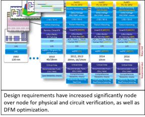
In general, advanced process nodes have significantly more design constraints and rules to which the electronic design automation (EDA) tools must adhere. Examples of this include advanced parasitic extraction and analysis tools to handle the more complex interconnects as well as detailed stress analysis that may be needed to ensure the behavior of each transistor.
Additionally, as multi-patterning is required for the super small geometries, more work must be done by the EDA tools to ensure that the layout of a dense layer can be successfully split into multiple masks.
These new constraints translate into the hidden costs of new tools as well as training for the designers who use them. As designs get bigger, design team sizes are growing and along with that comes the need for more EDA tools. While it may be unfair to blame these costs on a shift in process node, they are in fact real costs that must be considered when planning a new design.
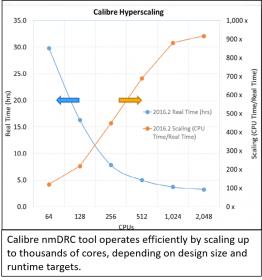
Coupling the larger number of constraints and rules, with larger teams and larger designs, the real kicker comes in the form of the amount of extra hardware required to process all the design and verification tasks. Arguably, some of the highest compute demands comes from the physical verification and modeling tools.
The more advanced the technology process the more advanced the modeling and design verification methods required. Many of the design verification steps are not even feasible without some kind of hyper-scaling capability. Fortunately for us, companies like Mentor are fielding products that can take advantage of hyper-scaling. Calibre nmDRC can scale up to thousands of cores. Without this we wouldn’t be able to do the kinds of system-on-chip (SoC) circuits that we do today.
The hidden cost here is the cost to provision and maintain large compute farms on which all the tools can be run. Some companies choose to provision these compute farms internally while others are looking to leverage the cloud. Either way, the cost is real. Thankfully these costs can be amortized over many designs, design tasks and process nodes.
Another key issue is the worry of sunk EDA tool investments. Will the company be able to continue to use the tools they purchased or will they need entirely new tools to handle the next process node? Along this vein, Mentor’s Calibre nmDRC team has done a great job of segregating and layering their capabilities to ensure that a company’s previous investments in their tools are not lost when migrating to a new process node. Calibre’s capabilities and features are set up so that advanced functionality can be added on an as-needed basis. Core features required by all foundries are grouped and preserved in the base capabilities of the tool while features such as multi-patterning, pattern matching, advanced fill technology, and advanced reliability checking can be readily added to the base features when and as they are needed.
In summary, the trade-offs for shifting to a new process node comes down to comparing higher NRE costs associated with the newer process node versus the expected return on investments derived from enhanced chip performance, reduced bill of materials through integration and lower overall unit prices. The good news for designers looking to move to more advanced process nodes is that the EDA providers like Mentor continue to improve their tool capabilities and performance while making it economically feasible to add capabilities as you go.
See also:
Mentor White Paper for more details
Mentor Calibre nmDRC products


Comments
4 Replies to “Whitepaper : The True Costs of Process Node Migration”
You must register or log in to view/post comments.