Last month I did an article about Intrinsix and their Ultra-Low Power Security IP for the Internet-of-Things (IoT). As a follow up to that article, I was told by one of my colleagues that the article didn’t make sense to him. The sticking point for him, and perhaps others (and that’s why I’m writing this article) is that he couldn’t see why you would want hardware acceleration for security in IoT edge devices. He wasn’t arguing the need for security. He was simply asking why you would spend the extra hardware area in a cost-sensitive device when you could just use the processor you already have in the device to do the work in software.
I thought this was a good question and one that needed more than a flippant answer from me, so I went back to Intrinsix and had an interesting discussion with Chuck Gershman, director of strategic development at Intrinsix. It turns out the short answer is “power.” Edge devices spend a large percentage of their life not doing much. Many of the newest edge devices run off the tiniest of batteries and use energy harvesting from vibrations, pressure, light, etc. to fuel themselves. To do this, however, they must literally be able to shut themselves down for long periods of time.
So, how do security accelerators help? Well, most IoT edge devices that use their CPUs for security tasks don’t really shut down. They go into a sleep mode that keeps system registers alive so that they don’t lose device state. If you lose device state, the device must do a secure boot when it is time to wake up, and that takes CPUs both time and energy.
Intrinsix has shown that by using their hardware accelerated IP, they can fully shut down the device and then do a secure reboot in milliseconds instead of multiple seconds it takes a CPU to do the same thing. By using a dedicated hardware accelerator, they can boot the system up to 800 times faster, and the amount of power saved by being fully shut down instead of simply sleeping can lead to a 1000X power reduction and up to 10X better battery life.
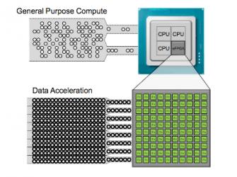
Not to be totally rebuffed, my colleague then made the point that we were talking about IoT edge devices that were supposed to cost in the sub $1 / device range (in some cases in the pennies per device range). Hardware accelerators implied bigger die which means higher costs. In one sense my colleague was correct. It’s well known that cloud servers and IoT network hubs are expected to have lots of encrypted traffic as the cloud servers could be dealing with hundreds of network hubs, and the network hubs could be dealing with thousands of edge devices. One would expect to see dedicated security hardware in these devices to handle all the secure connections. The edge device, however, is likely only to be talking to just a few or maybe only one network hub.
Time for another discussion with Chuck who was all too happy to explain that the beauty of the Intrinsix security IP was that it was highly scalable. It turns out when Intrinsix designed their IP, they used an architecture that let them use configurable parallel computing for the security features. This means that they can optimize the design to meet different power, performance, and area (PPA) trade-offs while still giving you the benefit of having hardware acceleration.
So, you can still get the power benefits provided by the accelerators while having a minimal area penalty (which could be insignificant depending on the silicon technology used, pinout and package). And, since the IP is configurable, you can optimize the IP for whatever work load the device is expected to see. For network hubs and servers that means you can significantly boost their performance by adding more parallel compute lanes in the IP.
Last statement from my doubting colleague, was “Ok, so it sounds like I have to be a security guru to know how to optimize this IP to make the implied trade-offs”. For this one, I already knew the answer, which was, “no, you don’t.” Intrinsix is a design services firm that has the platforms, process, and people required to ensure first-turn success of your semiconductor project. They already have security expertise in-house and the necessary knowledge to optimize the IP for you. You tell them what you are trying to do and they can generate a fully optimized security IP for the job that is ready to drop into your ASIC. And… If you so desire, they can also help you to embed the IP into your ASIC or do the entire ASIC as well.
So, for those readers who had the same doubts as my colleague, I hope this article has cleared things up. Of course, if you want more details the Intrinsix team will be happy to talk to you.
If you want to learn more about Intrinsix and their IoT offerings, you can find them online at the link below. You may also want to download their IoT eBook.
See also:
eBook: IoT Security The 4[SUP]th[/SUP] Element
Intrinsix Fields Ultra-Low Power Security IP for the IoT Market
Intrinsix Website