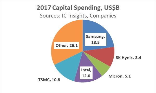
RVN! 26 Banner revised (800 x 100 px) (600 x 100 px)

Designing at 7nm with ARM, MediaTek, Renesas, Cadence and TSMC

Designing at 7nm with ARM, MediaTek, Renesas, Cadence and TSMC
by Daniel Payne on 07-11-2017 at 12:00 pm

The bleeding edge of SoC design was on full display last month at DAC in Austin as I listened to a panel session where members talked about their specific experiences so far designing with the 7nm process node. Jim Hogan was the moderator and the panel quickly got into what their respective companies are doing with 7nm technology already. Earlier this year we heard about the first 10nm chip being used for the Qualcomm Snapdragon 835 chip, so I was quite interested to here what the next smaller node at 7nm was going to bring us.

Continue reading “Designing at 7nm with ARM, MediaTek, Renesas, Cadence and TSMC”


Synopsys New EV6x Offers 4X More Performance to CNN

Synopsys New EV6x Offers 4X More Performance to CNN
by Eric Esteve on 07-11-2017 at 7:00 am

When Synopsys bought Virage Logic in 2010, ARC processor IP was in the basket, but at that time ARC processor core was not the most powerful on the market, and by far. The launch of EV6x vision processor sounds like Synopsys has moved ARC processor core by several orders of magnitude in term of processing power. EV6x deliver up to 4X higher performance on common vision processing tasks than the previous generation, delivering up to 4.5 TMAC/s in 16nm process.

In fact, even if EV6x is part of ARC CPU IP family, this vision processor is a completely new product, defined to address high throughput applications such as ADAS, video surveillance and virtual/augmented reality. If an architect is still hesitating between CPU, GPU, H/W accelerator or DSP based solution, both the performance, power efficiency and flexibility of such solution like EV6x should greatly ease the decision.

Why does Convolutional Neural Network (CNN) becoming key part of a vision processor? Because CNN is supporting deep learning and this approach outperforms other vision algorithms. Attempting to replicate how the brain sees, CNN recognizes objects directly from pixel images with minimal pre-processing. If we look at the relative performance of the various algorithm since 2012 and compare the result with human error, we notice two important points. Since 2014, Deep Convolutional Network algorithm are giving better result than human, moreover, the deeper the network, the better is will be, see ResNet with 152 layers. We can also derive from this evolution across time the fact that for such very fast-moving technology, flexibility is mandatory and that customer designed solutions based on H/W accelerator are quickly become obsolete…

But the latest vision requirements need increasing computational bandwidth and accuracy. Image resolution and frame rate requirements have moved from 1MP at 15 fps to 8MP at 60 fps, and the neural network complexity is greatly increasing, from 8 layers to more than 150 layers. That’s why the new EV6x has been boosted, delivering up to 4.5 TMAC/s, keeping in mind the power consumption. For CNN, the power efficiency is up to 2,000 GMAC/s per Watt in 16nm FinFET technology (worst case conditions). Because performance is key, architects can integrate up to four vision CPU for scalable performance and vision CPU supports complex computer vision algorithms including pre -and post- CNN processing.

Synopsys has used techniques to reduce data bandwidth requirements, and decrease power consumption. For example, the coefficient and feature map are compressed/decompressed. The EV6x solution include CNN engines using 12-bit computations, leading to less power and area but with the same accuracy as 32-bit floating point. This is a wise choice, if you consider that a 12-bit multiplier is almost half the area of a 16-bit multiplier! To be ready for the next technology jump, the EV6x supports neural networks trained for 8-bit precision… and we have seen that CNN vision is a fast moving domain.

For vision, CNN can be used to process multiple tasks, like image classification, search for similar images, or object detection, classification and localization. These tasks are supporting automotive ADAS systems, for example, but not only. EV6x vision processor will support surveillance application as well as drones, virtual or augmented reality, mobile, digital still camera, multi-function printers, medical… and probably more to come!

Availability
The DesignWare EV61, EV62 and EV64 processors are scheduled to be available in August 2017. The MetaWare Development Toolkit and EV SDK Option (which includes the OpenCV library, OpenVX runtime framework, CNN Graph Mapping tools and OpenCL C compiler) are available now.

From Eric Esteve from IPnest


Mentor & Phoenix Software Shed Light on Integrated Photonics Design Rule Checking

Mentor & Phoenix Software Shed Light on Integrated Photonics Design Rule Checking
by Mitch Heins on 07-10-2017 at 12:00 pm

Just prior to the opening of the 54[SUP]th[/SUP] Design Automation Conference, Mentor, a Siemens company, and PhoeniX Software issued a press release announcing a new integration between their tools to help designers of photonic ICs (PICs) to close the loop for manufacturing sign-off verification. This is a significant piece of the overall flow puzzle that up till now has been missing. While at the conference, I was able to sit in on a presentation and demonstration to get first impressions of the new flow.


Anyone who has ever taped out a PIC knows it’s prudent to leave time in the schedule to work through a host of false violations seen by foundries trying to use standard CMOS design rule checks for photonics. Curvilinear PIC layouts are particularly challenging for design rule checking (DRC) and logic vs schematic (LVS) applications due to curvilinear shapes represented in GDSII as multi-point polygons.

To get a feel for the amount of errors one might have to wade through, Mentor and PhoeniX used a typical photonic layout module known as a 90-degree hybrid used for communications protocols like QPSK. They had Calibre run both a normal CMOS DRC deck and an Equation-based DRC deck on the layout and compared violations found. The results were astounding with 6,420 errors flagged by the regular deck and only 15 flagged by the Equation-based rule deck. The 15 violations found by the equation-based rule deck were real errors. The rest were not. Lest anyone think this is a demo set up to make a point – well, it is – but I can also tell you it is quite indicative of what you would see in real life. Remember this isn’t even a full chip. It’s only a small module or part of a photonics chip.

Foundries are working to upgrade their DRC decks to use more of Calibre’s advanced features such as pattern matching and equation-based design rule checking to reduce the number of false errors flagged. However, even with these changes, the DRC runs are still being done at the foundry right before fabrication which means that real problems are still being found far too late in the design cycle where changes are expensive.


A better solution would be one where the sign-off rule checks could be done incrementally during the design process so that any required circuit changes could be quickly made without having to re-engineer the entire layout. Most PIC design flows today use PhoeniX Software’s OptoDesigner platform for layout synthesis. While OptoDesigner does a great job of correct-by-construction layout, designers are now moving from photonic module development to full blown photonic circuit layout and in that effort, they are cutting corners to create smaller more area-efficient designs which can inevitably cause inadvertent design rule violations.

The integration between OptoDesigner and the Calibre nm Platform enables designers to run Calibre verification directly from the OptoDesigner design tool using the Calibre Interactive GUI. Results can then be viewed in OptoDesigner using the Calibre RVE results viewing environment. The Calibre RVE interface enables violation highlighting, zooming, waiver management and error debugging, all while making corrections in OptoDesigner. This was shown live in the demo as the final 15 real errors were quickly changed in OptoDesigner and Calibre was run in real time showing a clean result.

OptoDesigner can also import the Calibre results directly into the tool, if the designer so desires. The interface was developed by PhoeniX Software through Mentor’s OpenDoor program, a mechanism that supports the development, certification, and distribution of interfaces among EDA vendors to promote open interoperability.

The new interface brings some much-needed formalism to the verification of PIC layout for manufacturing design rules. Additional work is underway between the two companies to formalize a better mechanism for photonic LVS. This is still early days for PIC LVS as most PIC designers are still doing the design in a layout tool as opposed to a schematic, but this too is changing as PICs become more complex.


Mentor Calibre is also quite famous for its ability to model manufacturing effects such as Chemical Mechanical Polishing (and the requisite fill patterns needed for it) as well as lithography. These areas look to be natural extensions to the work already done by Mentor and PhoeniX Software. While photonic curvilinear shapes are large in comparison to electronic components, such as FinFet transistors, the performance of the photonics is highly susceptible manufacturing variations such as differences in layer thicknesses and the fidelity of the printed curved shapes.

Calibre SmartFill is Mentor’s tool for handling constraint-driven fill. SmartFill can be used to post-process the design layout to add foundry-specified metal-fill that meets density targets needed to ensure good layer planarity and thickness control while at the same time ensuring that the fill does not impact optical behavior of the photonic circuit.

Similarly, Calibre LFD (Litho Friendly Design) is Mentor’s tool for simulating the patterned shapes based on the lithography setup of the foundry. Resulting contours from simulations can be used to analyze the impact of lithography printing effects such as rounding and pinching on the photonic device. Used in conjunction with OptoDesigner, these capabilities would enable designers to adjust the layout prior to tape-out to counter any negative impacts the lithography may have on the design.

All in all, this was a very impressive presentation and demonstration that was well received by those attending the session. It appears that the design flows for integrated photonics are coming together nicely.

See also:
Mentor / PhoeniX Software Press Release
Mentor Calibre nm Platform Product Page

PhoeniX Software OptoDesigner Product Page


Cadence Explores Smarter Verification

Cadence Explores Smarter Verification
by Bernard Murphy on 07-10-2017 at 7:00 am

Verification as an effectively unbounded problem will always stir debate on ways to improve. A natural response is to put heavy emphasis on making existing methods faster and more seamless. That’s certainly part of continuous improvement but sometimes we also need to step back and ask the bigger questions – what is sufficient and what is the best way to get there? Cadence hosted a panel at DAC this year on that topic, moderated by Ann Mutschler of SemiEngineering. Panelists were Christopher Lawless (Intel Director of customer-facing pre-silicon strategies), Jim Hogan (Vista Ventures), Mike Stellfox (Cadence fellow) and David Lacey (Verification scientist at HP Enterprise). I have used Ann’s questions as section heads below.

What are the keys to optimizing verification/validation?
Chris said that the big challenge is verifying the system. We’re doing a good job at the unit level, both for software and hardware components, but complexity at the (integrated) system level is growing exponentially. The potential scope of validation at this level is unbounded, driving practical approaches towards customer use-cases. David highlighted challenges in choosing the right verification approach at any point and how best to balance these methods (e.g. prototyping versus simulation). He also raised a common concern – where is he double-investing and are there ways to reduce redundancy?

Jim saw an opportunity to leverage machine learning (ML), citing an example in a materials science company he advises. He sees potential to mine existing verification data to discover and exploit opportunities that may be beyond our patience and schedules to find. Mike echoed and expanded on this saying that we need to look at data to get smarter and we need to exploit big data analytics and visualization techniques, along with ML.

Of the verification we are doing today, what’s smart and what’s not?
David said a big focus in his team is getting maximum value out of the licenses they have. Coverage ranking (of test suites) is one approach, cross coverage ranking may be another approach. Mike said that formal is taking off, with interest in using these methods much earlier for IP. And that creates need to better understand the coverage contribution and how that can be combined with simulation-based verification. He added that at the system level, portable stimulus (PS) is taking off, there’s more automation appearing and it is becoming more common to leverage PS across multiple platforms. Chris was concerned about effectiveness across the verification continuum and wanting to move more testing earlier in that continuum. He still sees need for hardware platforms (emulation and prototyping) but wants them applied more effectively.

What metrics are useful today?
Chris emphasized that synthetic testing will only take you so far in finding the bugs that may emerge in real OS/applications testing. Real workloads are the important benchmark. The challenge is to know how to do this effectively. He would like to see ML methods extract sufficient coverage/metrics from customer use-cases ahead of time, and to propagate appropriate derived metrics from this across all design constituencies to help each understand impact on their objectives.

Mike felt that, while it may seem like blasphemy, over-verifying has become a real concern. Metrics should guide testing to be sufficient for target applications. David wants to free up staff earlier so they can move on to other projects. In his view, conventional coverage models are becoming unmanageable. We need analytics to optimize coverage models to address high-value needs.

Is ML driving need for new engineers?
Jim, always with the long view, said that the biggest engineering department in schools now is CS, and that in 10 years it will be cognitive science. He believes that we are on cusp of cognitive methods which will touch most domains. Chris wouldn’t commit to approaches but said Intel is exploring ways to better understand and predict. He said that they have many projects stacked up and need to become more efficient, for example in dealing with diverse IoT devices.

David commented that they are not hiring in ML but they are asking engineers to find new ways to optimize, more immediately to grow experience in use of multiple engines and to develop confidence that if something is proven in one platform, that effort doesn’t need to be repeated on other platforms. Following this theme, Chris said that there continues to be a (team) challenge in sharing data across silos in the continuum. And Mike added that, as valuable as UVM is for simulation-centric work, verification teams need to start thinking about building content for multiple platforms; portable stimulus is designed to help break down those silos.

Where are biggest time sinks?
David said, unsurprisingly, that debug is still the biggest time sink, though the tools continue to improve and make this easier. But simply organizing all the data, how much to keep, what to aggregate, how to analyze it and how to manage coverage continues to be a massive problem. This takes time – you must first prioritize, then drill down.

Chris agreed, also noting the challenge in triage to figure out where issues are between silos and the time taken to rewrite tests for different platforms (presumably PS can help with this). Jim wrapped up noting that ML should provide opportunities to help with these problems. ML is already being used in medical applications to find unstructured shapes in MRI data – why shouldn’t similar approaches be equally useful in verification?

My take – progress in areas we already understand, major moves towards realistic use-case-based testing, and clear need for big-data analytics, visualization and ML to conquer the sheer volume of data and ensure that what we can do is best directed to high-value testing. I’ll add one provocative question – since limiting testing to realistic customer use-cases ensures that coverage is incomplete, how then do you handle (hopefully rare) instances where usage in the field strays outside tested bounds? Alternatively, is it possible to quantify the likelihood of escapes in some useful manner? Perhaps more room for improvement.


Exclusive – GLOBALFOUNDRIES discloses 7nm process detail

Exclusive – GLOBALFOUNDRIES discloses 7nm process detail
by Scotten Jones on 07-08-2017 at 7:00 am

In a SemiWiki EXCLUSIVE – GLOBALFOUNDRIES has now disclosed the key metrics for their 7nm process. As I previously discussed in my 14nm, 16nm, 10nm and 7nm – What we know now blog GLOBALFOUNDRIES licensed their 14nm process from Samsung and decided to skip 10nm because they thought it would be a short-lived node. At 7nm GLOBALFOUNDRIES has taken advantage of the additional technical resources they acquired from IBM to develop their own process.


GLOBALFOUNDRIES 7LP
As Dan Nenni previously discussed in his GlobalFoundries 7nm and EUV Update! blog 7LP (Leading Performance) will offer a greater than 40% performance improvement relative to 14nm or greater than 60% lower power. Area scaling will be approximately 2x and the die cost reduction will be greater than 30%, with greater than 45% in target segments. Initial customer products on 7LP are expected to launch in the first half of 2018 with volume production in the second half of 2018.

The 7LP process will be produced with optical lithography and what we now know is the Contacted Poly Pitch (CPP) will be 56nm and the Minimum Metal Pitch (MMP) will be 40nm produced with Self-Aligned Double Patterning (SADP). A 6-track cell will be offered with a cell height of 240nm. The high density 6T SRAM cell size is 0.0269 microns squared. A 7LP+ process is also planned that will take advantage of EUV when it is ready to offer improved performance and density.

GLOBALFOUNDRIES is also in the unique position of providing an in-house ASIC platform FX-7 on their 7LP process. FX-7 provides a comprehensive suite of tailored interface IP including High Speed SerDes (60G, 112G), differentiated memory solutions including low-voltage SRAM, high-performance embedded TCAM, integrated DACs/ADCs, ARM processors, and advanced packaging options such as 2.5D/3D

Comparison to other processes

In my 14nm, 16nm, 10nm and 7nm – What we know now blog I looked at Intel’s 10nm process compared to Samsung and TSMC’s 7nm processes. Due to the lack of available information on GLOBALFOUNDRIES 7nm process I didn’t include it, I can now add it to the comparison but first I need to make a few updates to the data previously discussed.

Previously I used a 44nm CPP for Samsung basing it off the IBM, Samsung, GLOBALFOUNDRIES IEDM 2016 paper. I am now hearing their actual CPP is 54nm. Of the 4 processes being compared Samsung is the only process that will use EUV initially and therefore the process has the latest risk production date of the four and likely the highest risk of missing that date (something Samsung appears to recognize with their recent announcement of an optically based 8nm process due to enter risk production in late 2017). The use of EUV should result in a lower mask count that the competing processes and we are currently forecasting Samsung will use EUV for contacts, vias and metal block masks as part of a Self-Aligned Quadruple (SAQP) Patterning scheme for 1x metal layers.

In the same article, I used 54nm for TSMC’s CPP and although that is a claimed value for the process, I am hearing that their actual libraries have a 57nm CPP.

The following table compares the latest data we have for 10nm/7nm:

[INDENT=2]
[INDENT=2][1] IC Knowledge estimates.
[INDENT=2]Table 1. 10nm/7nm process comparison.

The data in the table illustrates the need for design-technology co-optimization (DTCO) at the leading edge. Intel and Samsung have the smallest CPP and MMP values but because GLOBALFOUNDRIES and TSMC offer 6T cells, they achieve smaller cell heights and ultimately GLOBALFOUNDRIES has the smallest CPP x Cell Height value. Samsung achieves the smallest SRAM cell size and through the use of EUV we expect Samsung to have the lowest mask count.

Conclusion
GLOBALFOUNDRIES 7LP adds a competitive 7nm process to customer options for leading edge design and production. The process parameters are competitive across the board and provide leading density. The availability of the FX-7 ASIC platforms offers customers an additional engagement path not available at other foundries.


Embedded FPGA’s create new IP category

Embedded FPGA’s create new IP category
by Tom Simon on 07-07-2017 at 12:00 pm

FPGA’s are the new superstar in the world of Machine Learning and Cloud Computing, and with new methods of implementing them in SOC’s there will be even more growth ahead. FPGA’s started out as a cost effective method for implementing logic without having to spin an ASIC or gate array. With the advent of the web and high performance networking hardware, discrete FPGA’s evolved into heavy duty workhorses. The market has also matured and shaken out, leaving two large gorillas and a number of smaller players. However, the growth of AI and the quest for dramatically improved cloud server hardware seems to be the expanding the role of FPGA’s.


At DAC in Austin I came across Achronix a relatively new FPGA company that is experiencing a renaissance. I stopped by the speak to Steve Mensor, their VP of Marketing. There was reason enough to speak with him because of their recent announcement that their YTD revenues for 2017 are already over $100M. This is largely the result of solid growth in their Speedster 22i line of FPGA chips. Achronix originally implemented this line at the debut of Intel’s Custom Foundry on the then state of the art 22nm FinFET node. This gave them the distinction of being the first customer of Intel’s Custom Foundry.


Building on this, Steve was eager to talk about their game changing IP offering of embedded FPGA cores – aptly named Speedcore eFPGA. These are offered as fully customized embedded FPGA cores that can be integrated right into system level SOC’s. To understand why this important, we have to look at a recent research project by Microsoft called Catapult with the goal of significantly boosting search engine performance. Microsoft discovered that there was a big advantage in converting a subset of the search engine software into hardware optimized for the specific compute operation. This advantage is amplified when these compute tasks can be made massively parallel – exactly the kind of thing that FPGA’s are good at. They also studied the same approach for cloud computing with Azure and found performance benefits there too.

The next market factor that starts to make embedded FPGA cores look extremely attractive is Neural Networks. Both training and recognition require massive computing that can be broken into parallel operations. The recognition phase – such as the one running in an autonomous vehicle – can be implemented largely with integer operations. Once again this aligns nicely with FPGA capabilities. So if FPGA’s can boost search engine and AI applications, what are the barriers to implementing them in today’s systems?

If you look at the current marketing materials for Altera and Xilinx you can see that they dedicate a lot of energy to developing and promoting their IO capabilities. Getting data in and out of an FPGA is a critical function. Examining the floor plan for an FPGA chip, you will see a large area used for programmable IO’s. Of course along with the large areas resources used, comes the need for higher power consumption.


Embedding an eFPGA core means that interface lines can be directly connected to the rest of the design. With less area for each signal, wider busses can be implemented. Interfaces can run faster, now that interface SI and timing issues have been reduced with on-chip integration.

The other benefit alluded to earlier is that eFPGA can be configured to achieve optimal performance. The adjustable parameters include the number of LUT’s, embedded memories and DSP blocks. Customers get GDS II that is ready to stitch into their design. The tool chain for Speedcore eFPGA’s can accommodate the custom configurations.


Steve told me that today the largest share of their impressive revenue is standalone chips, but by 2020 he expects 50% of their sales to be embedded. Another application for FPGA’s is use as chiplets for 2.5D designs. But more on that in future writings.

Steve emphasized that designing FPGA’s is pretty tricky. There are power and signal integrity issues that need to be solved due to their massive interconnect. Real improvement only comes over time with years of experience optimizing and tuning architecture. Steve suggested that many small improvements over time have added up to much better results in their FPGA’s.

Right now it looks like Achronix is positioned to break away from the pack of smaller FPGA providers and potentially revolutionize the market. With this new appproach, FPGA’s can be said to have decisively transitioned from their early days of being a glue logic vehicle to a pivotal component of advanced computing and networking applications. For more details on Achronix eFPGA cores take a look at their website.


LETI Days 2017: FD-SOI, Sensors and Power to Sustain Auto and IoT

LETI Days 2017: FD-SOI, Sensors and Power to Sustain Auto and IoT
by Eric Esteve on 07-07-2017 at 7:00 am

I have attended last week to the LETI Days in Grenoble, lasting two days to mark the 50[SUP]th[/SUP] anniversary of the CEA subsidiary. Attending to the LETI Days is always a rich experience: LETI is a research center counting about 3000 research engineers, but LETI is also a start-up nursery. The presentations are ranging from high level communication, to panels involving actors from the semiconductor and electronics industry (like “Future Applications and New Technologies” with Rajesh PANKAJ, Qualcomm, Alain MUTRICY, Globalfoundries and Antun DOMIC, Synopsys) or start-up sessions, all the start-up being issued from LETI!

We also had a very interesting keynote presentation from Jean-Marc CHERY, STMicroelectronics, passing a very realistic message to the industry. STM doesn’t play anymore in the smartphone application processor game, this market is dominated by Samsung, Apple and the Chinese chipmakers for the design side, and by a couple of foundries (TSMC, Samsung …) heavily investing to support the most advanced FinFET nodes, but sensors from STM are integrated in the major smartphones. STM is now developing innovative technology to support new power electronics devices, like SiC (Silicon Carbide) and supporting automotive with plenty of new devices, going up to ADAS through Mobileye support on FDSOI.

Instead of burning cash trying to stay in the very competitive race for maximum integration (application processors for smartphones, set-top-box, etc.), capitalize in the company strengths with sensors, microcontrollers, power electronics to address highly growing markets (automotive, industrial IoT) looks like a wise decision from a mature semiconductor company… who is also a start-up issued from LETI long time ago (1972)!

The next event was the press conference given by Marie SEMERIA, CEA-LETI CEO and Fraunhofer Group for Microelectronics Chairman Hubert LAKNER, who just signed an agreement to “…develop next generation microelectronics to strengthen European strategic and economic sovereignty.” This announcement is linked with the recent billion euros investment from Bosch to build a 12” wafer fab in Dresden to deliver chips for IoT and mobility, back up by the German government as well as a €300 million investment recently made by the French government in microelectronic…

We (the press) have carefully heard Marie Semeria and Hubert Lakner explain that the collaboration will focus on specific R&D projects like:

– Silicon-based technologies for next generation processes and products, including design, simulation, unit process as well as production techniques
– Extended More than Moore technologies for sensing and communication applications
– Advanced-packaging technologies

That I like with press conferences, by opposition to keynotes talk, is that you can ask for clarification after the talk. My question was about the level of investment made in semiconductor in Europe, to be compared with the $100 billion claimed by the Chinese government, or even this made by TSMC in Taiwan to build a new fab for FinFET – in the $10 billion range for a single fab!

The answer from Marie Semeria was frank, and very interesting. She said that European electronics and semi companies are no more involved into the smartphone race, and shouldn’t try to pursue Moore’s law up to the technology limit, this is simply requiring too much cash. Let’s try to be realistic, and develop the technologies supporting the applications and systems where the European industry is strong, namely FDSOI, sensors and power devices.

This strategy will allow to go up in the value chain and manufacture in Europe the systems based on the above-mentioned devices or technologies. At this point, you may want to make a comparison with IMEC, the well-known Belgium research center. IMEC is involved into the development of the most advanced technologies (Moore’s law), and do it very well. Unfortunately, these technologies are transferred to wafer fab and semiconductor companies based out of Europe…

FD-SOI: Power consumption, Performance and Cost
FDSOI technology can be a key differentiator, GlobalFoundries is implementing fabs supporting 22FDX and 12FDX in Europe, thanks to the licensing agreement with LETI.

Sensors
Many emerging applications, like ADAS in automotive or Industrial IoT, require more and more sensors. The next step is to put intelligence into sensors. Companies like STMicroelectronics are focusing on sensors and ship everywhere, including to the European industry.

Power Electronic
These devices will be more and more used, for example with the development of electric cars or industrial equipment and IoT. Europe is well positioned both in automotive and industrial segments. See also STM investment into SiC.

To conclude, I would like to remind you the development of LiOT by LETI. LiOT is an IP platform that developers could use to design ASIC for their IoT applications. I saw a paper from LETI during IP-SoC in Grenoble and it was very good, so I have suggested to LETI to present a paper describing LiOT during the DAC in Austin. This paper was well received by the audience and demonstrate LETI strong involvement into IoT.

And this paper was good enough to obtain the “DAC Best Paper Awards” in the Design/IP track category!

From Eric Esteve from IPNEST


Webinar: Synopsys on Clock Gating Verification with VC Formal

Webinar: Synopsys on Clock Gating Verification with VC Formal
by Bernard Murphy on 07-06-2017 at 12:00 pm

Clock gating is arguably the mostly widely-used design method to reduce power since it is broadly applicable even when more sophisticated methods like power islands are ruled out. But this style can be fraught with hazards even for careful designers. When you start with a proven-correct logic design and add clock gating, the logic (and timing) can change in ways which are not an intuitively simple extension of the original design, raising the need to validate that those changes have not broken the logic intent.

REGISTER HERE for Webinar on July 11[SUP]th[/SUP] at 10am PDT

The problem sounds similar to validating that synthesized logic is functionally equivalent to original RTL and we know how to deal with that problem – run logic equivalence checking between the RTL and the synthesized netlist. But that doesn’t work for clock gating checks because conventional equivalence checking (mostly) checks combinationallogic equivalence between reference points. However, clock gating structures are inherently sequential; traditional equivalence engines don’t work with this kind of problem – you need to use sequential equivalence checking (SEQ), still a formal-based check but allowing for cycle-shifted equivalence.

Why not simply use dynamic verification to verify the correctness of this gating? You could but (a) you have to extend your testbenches to add directed tests for clock-gating, not only increasing the complexity of testing but also dramatically increasing verification run-times and (b) you have to consider all possible variations of switching versus functionality in each case. Or you could verify formally, which doesn’t impact your dynamic verification setup or run-times at all and is intrinsically complete. And, by the way, VC Formal SEQ is an app, so much easier to use than traditional formal. Hmm – which way to go? Maybe you should check out the webinar.

REGISTER FOR THIS WEBINAR to learn how you can use VC Formal to formally verify the sequential equivalence of a clock gated circuit with the original logic, to have full confidence that your logic intent has been preserved.


ADAS and Vision from Cadence

ADAS and Vision from Cadence
by Daniel Payne on 07-05-2017 at 12:00 pm

A huge theme at #54DAC this year was all things automotive and in particular the phrase ADAS (Assisted Driver Assistance Systems), so I followed up with Raja Tabet a corporate VP of emerging technology at Cadence. We met on Monday in a press room where I quickly learned that Cadence has been serving the automotive industry for the past 15 years with IC tools, IP and services.

Cadence acquired Tensilica back in March 2013, gaining instant access to an app-specific acceleration platform with DSP features that was easy to customize, generated SW, and custom instructions. This technology fits quite well with ADAS features for vision, radar, Lidar and even sensor fusion. I’ve been following Tensilica over the years because my former roommate Chris Rowen founded the company, and we both worked at Intel starting in 1978.

Related blog – A Brief History of Tensilica

The latest version of Tensilica (P6) supports both imaging and vision functions. The Vision C5 is a CNN (Convolution Neural Network) processor, recently announced that gives you 1TMAC/sec computational capacity. What makes the C5 a bit unique is that in a single chip you get both a CNN and CPU together, instead of separate components from different vendors. Here’s a quick snapshot of the Tensilica product offerings:

Customers would first conceive of a neural network for their application, train the network, then embed the network using software to compile it into Tensilica hardware. Competitive approaches in this space include vendors that use GPUs or hardware accelerators. With the approach in the C5 you get a power/performance metric that is quite high and is easy to program. With Cadence you now have the technology to create your own ADAS system.

Related blog – Cadence to acquire Tensilica

The automotive infotainment world is well served by standards, however ADAS is so new that there are no standards out their to quickly choose from. Expect defacto standards to begin emerging as automotive companies form alliances or adopt specific vendor tools and flows.

Related blog –CPU, GPU, H/W Accelerator or DSP to Best Address CNN Algorithms?

From a design viewpoint there’s a lot to consider for the automotive market, like:

  • Functional safety
  • Compliance with the ISO26262 requirements, ASIL A to ASIL D
  • Fault simulation
  • Static and formal analysis
  • Fault analysis with emulation

The technology at Cadence has matured to the point of offering a comprehensive methodology for automotive design. Adjacent to the automotive market is a related market for robotic technology where imaging and vision are fundamental requirements for industrial robots. What intrigues me the most about neural networks is the ability for the machine to get smarter with each new encounter, or a new release of firmware that is downloaded over a wireless network.

Related blog – The CDNLive Keynotes

Along the path to fully autonomous driving which is level 5, are the four lower levels of automation. No matter which level you are trying to design for there are common questions:

  • Which architecture is the best one?
  • Centralized sensors or distributed intelligence per sensor?
  • Hybrid architecture?

The approach at Cadence is to let you decide how you want to implement ADAS by making your own decisions. In 2017 there are some 17 ADAS events that Cadence will participate at, so this opportunity is large and growing, which is always a good thing.