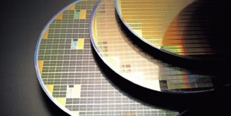
RVN! 26 Banner revised (800 x 100 px) (600 x 100 px)

Why Ansys bought CLKDA

Why Ansys bought CLKDA
by Bernard Murphy on 07-18-2017 at 7:00 am

Skipping over debates about what exactly changed hands in this transaction, what interests me is the technical motivation since I’m familiar with solutions at both companies. Of course, I can construct my own high-level rationalization, but I wanted to hear from the insiders, so I pestered Vic Kulkarni (VP and Chief Strategist) and Joāo Geada (Chief Technologist and previously CTO at CLKDA) into explaining their view of the background and benefits.


Ansys already has a strong position in integrity/reliability for electronic systems, from chip design up through the package and the board level. This is important, for example, in design for total system reliability and regulatory compliance in ADAS systems under challenging constraints such as widely varying temperature environments (in front of a windscreen in Death Valley, or in an unheated enclosure in Barrow, Alaska). Particularly at the chip-level, through their big data/elastic compute approach to fine-grained multi-physics analytics rather than margin-based analysis, they assert that they can offer higher-confidence in meeting integrity and reliability goals in reduced area with faster design turn-times. What they presented at DAC seems to bear this out.


This is an important advance, but as always in semiconductor design, the goal-posts continue to move. Vic and Joāo said that customers are finding increasing difficulty in getting to timing signoff at 16nm and below, often starting with 10k+ STA violations, which can take 3-4 weeks to close. They are managing process variation factors (OCV) though use of the latest standards for timing in Liberty models but there are also dynamic factors to consider. At these feature sizes, operating voltage can drop to 0.6-0.7V, but threshold voltages don’t drop as much, so sensitivity to power noise increases and that can lead to intermittent timing failures in what would otherwise appear to be safe paths. Equally, clock jitter as a result of power noise can cause intermittent failures.

Of course you could follow the standard path and over-design the power distribution network (PDN) to margin for worst possible cases across the die. But that over-design becomes increasingly expensive and uneconomic, especially at these aggressive nodes, so you settle for a compromise between area and risk in which you hope you covered the most likely corner cases. Based on presentations at DAC this year, Ansys has already demonstrated that they can replace this uncertain tradeoff in related problems with multi-physics analysis delivering low risk integrity/reliability across the die with significantly less over-design than the traditional approach.

Which bring us to the reason Ansys wanted the CLKDA FX tool-suite. To address these dynamic timing problems, they needed to fold a high-accuracy timer into their multi-physics analysis to enable analysis of timing side-by-side with dynamic voltage drops (DvD). The point here is to analyze locally across the design to guide local adjustment of the PDN where appropriate. In an area where there’s enough slack, maybe you’re not too worried if timing sometimes stretches out a bit, so there’s no need to upsize the local PDN. Where timing is tight, you upsize enough to ensure that DvD will not cause the path to fail. Similarly, multi-physics analysis will highlight where clock jitter sensitivity could cause failures and may require mitigation in the local clock distribution.

Getting this right requires an accurate timer, better than a graph-based STA, closer to Spice-level accuracy but much faster than Monte-Carlo Spice (MC Spice) so it can be effective on large designs. That of course has been the value-proposition of the FX family for many years – a technology which can propagate statistical arrival times and true waveform shapes while also maintaining correct distribution, yet run 100X faster than MC Spice. Since FX already has a bunch of customers, I have to believe that’s not just a marketing pitch 😎.

So where does this go next? I’m sure there will be continuing integration and optimization with the SeaHawk and Chip-Package-System flow. Joāo also pointed out a number of additional opportunities. Ansys’ strength is multi-physics analysis so there are opportunities to cross other factors in analysis – variability and timing or aging and timing for example. CLKDA has tilted at the variability windmill before, lobbying for a transistor-level static timing analysis approach, for example to better model the influence of accumulating non-Gaussian distributions along a path. Perhaps their concept will start to gain traction in this new platform. Their work in signoff for timing aging is also very intriguing and I think is likely to attract significant interest in high reliability/ long lifetime applications (automotive maybe?)

So now you know why Ansys acquired CLKDA. For me this seems like an even better home for the FX technology. You can learn more about ANSYS solutions, including the FX products, HERE.


HLS update from Mentor about Catapult

HLS update from Mentor about Catapult
by Daniel Payne on 07-17-2017 at 12:00 pm

I recall back in the late 1980’s when logic synthesis tools were first commercialized, at first they could read in a gate-level netlist from one foundry then output an optimized netlist back into the same foundry. Next, they could migrate your gate-level netlist from Vendor A over to Vendor B, giving design companies some flexibility in negotiating the best foundry terms. Finally, they could accept RTL code as an input, then create foundry-specific gate-level netlists that were optimized.

Since Synopsys came to dominate the RTL logic synthesis market in the 1990’s, many competitors have aimed to sit on top of logic synthesis with their own High Level Synthesis (HLS) tool. EDA vendors have tried over the years with varying degrees of commercial success to grow the HLS market. All of the big three in EDA have made inroads with HLS tools and sub-flows, so I met up with Badru Agarwala, GM at Mentor during DAC in Austin last month to get an update on what’s been happening with their Catapult product line.

Q: What are the industry trends with HLS these days?

A: HLS is only one pice of an ecosystem moving up to use the C++ language now, so one goal is to make C++ design as robust as RTL verification is.

Q: What customers are using HLS, has it gone mainstream yet?

A: Some big company names that you should recognize that are using HLS now include: NVIDIA, Qualcomm, Google and STMicroelectronics.

Q: Is there a sweet spot for using an HLS tool flow?

A: Yes, segments like machine vision, computer vision, 3D TV all enjoy an HLS methodology.

Q: What about design capacity with HLS, is that an issue?

A: We’ve seen a 25 Million gate design completed with Catapult, so the capacity is there.

Q: What benefits do HLS designers enjoy the most?

A: Three things that are common benefits include: Verification is more thorough, the design process is much faster than RTL, and designers can make more changes at the last minute of their projects.

Q: How is HLS impacting the verification process?

A: Now with HLS you can start verification much earlier than before, in parallel with the design process, then when the code is stable start to do RTL design.


Q: What are some of the challenges of coding with C++ for an HLS language and how is Catapult changing?

A: Most existing C++ tools are for SW developers, not really well suited for HW developers, so there’s not much linting or property checking going on. HLS users really need coverage tools, along with bit accuracy and loop unrolling. We just announced Catapult DesignChecks to help an HLS user find bugs while coding, so they don’t have to debug as much with simulation and synthesis. There’s both a static mode of DesignChecks for fast linting plus a formal engine for checking. These approaches don’t even require a testbench to be coded.

A second new tool we’re talking about is Catapult Coveragewhich gives you code coverage for C++ and enables faster closure of synthesized RTL. Designers can reach 100% C coverage, then start to do HLS synthesis. We’ve had coverage tools for gate-level and RTL, so it only makes sense to raise that up to the C level too.

We also have SLEC (Sequential Logic Equivalence Checking) HLS a new C to RTL equivalence tool, so that you know that the RTL coming out of Catapult really is the same as the C++ that went into it, without having to run simulation and verification cases. Setup is more automated now.

Summary
Mentor with the Catapult family of tools has been at this HLS methodology for a long while now and have continued to invest in making the whole tool flow more integrated and easier to use for digital designs. I was impressed with the three StreamTV engineers in the Mentor booth who showed a 3D TV design using Catapult in their 15 month project because of how few people were required to do such a complex design so quickly, and consumers view 3D without glasses.


NetSpeed’s Pegasus Last-Level Cache IP Improves SoC Performance and Reduces Latency

NetSpeed’s Pegasus Last-Level Cache IP Improves SoC Performance and Reduces Latency
by Mitch Heins on 07-17-2017 at 7:00 am

Memory is always a critical resource for a System-on-Chip (SoC) design. It seems like designers are always wanting more memory, and the memory they have is never fast enough to keep up with the processors, especially when using multi-core processors and GPUs. To complicate matters, today’s SoC architectures tend to share memory across heterogeneous environments including temporal (isochronous, steady, random) and functional (fully coherent, IO-coherent and non-coherent) features. System designers are forever trading off performance and latency against the sharing of memory resources, power reduction and ensuring system timing integrity.

Many designers are now turning to what is known as last-level cache (LLC) to avoid SoC memory access bottlenecks and congestion among heterogeneous masters. Some designers primarily think of a LLC as simply a L3 cache, however the people at NetSpeed have taken the LLC concept to a much higher level. Pegasus is the product name for NetSpeed’s LLC IP and when used in combination with NetSpeed’s NocStudio design software, Pegasus can be used to optimize circuit throughput, reduce latency and improve memory efficiency.

Pegasus is a parameterized and configurable LLC architecture that is layered over NetSpeed’s Orion and Gemini Network-on-Chip (NoC) technologies. Pegasus leverages NetSpeed’s core NoC capabilities to ensure quality of service (QoS) and deadlock avoidance while also allowing the designer to support coherent, non-coherent and mixed architectures. The IP provides support for design-time programmable coherent-cache and coherent-memory modes along with memory error-correcting code (ECC) capabilities.

Pegasus also features runtime modes that enable soft partitioning of cache associativity per master. This allows designers to better utilize their cache resources through integration of some system IPs and by enabling the use of some or all their LLCs as directly addressable RAM. This latter capability is particularly useful when having to support multiple applications processors on the SoC that differ in their RAM requirements.


A key feature of Pegasus is that the IP is both design and runtime programmable and it supports multiple modes including, coherent cache, reduced coherent latency, power reduction, memory cache, increased bandwidth through locality and improved software coherency by avoiding the need for flushes. Not all slave agents are created the same and having multiple LLCs, based on address ranges, gives designers the ability to customize each LLC based on the slave characteristics.

Pegasus also works with NocStudio’s understanding of the SoC’s floorplan to enable distributed LLCs which can aid in connectivity-congestion mitigation and improve overall system bandwidth and latency through locality. In addition, Pegasus can do all of this while working in coordination with ARM’s Trust Zone capabilities to ensure complete protection of a device from bad outside actors trying to breach the SoC’s key memory and code blocks. This is an essential feature for designs targeted at the Internet-of-Things (IoT) market.

Since Pegasus is used with NetSpeed’s NocStudio software many steps to configure and program the LLCs are automated making it easier for designers to incorporate Pegasus into their designs. Using NocStudio, designers can simulate their SoCs with different configurations of LLCs over different work-loads and expected traffic patterns to ensure latency and performance are optimized. This is important as coherent SoCs often have processors with conflicting needs and which may have some traffic flows that are highly sensitive to CAS latency while others are more sensitive to bandwidth requirements. Striking a balance in a heterogenous SoC is non-simplistic and Pegasus along with NocStudio makes the job a lot easier.


Not only can the Pegasus LLC IP help with system throughput, bandwidth and latency, it can also be used by designers to reduce their overall SoC power consumption. Pegasus enables better memory efficiency resulting in lower power consumption by removing unnecessary look-ups and making intelligent decisions on managing, optimizing, and accessing memory. A configurable LLC can be tailored to the specific characteristics of the DDR controller and can augment the optimizations of the controller by making smart decisions within the LLC.

Additionally, LLC RAM banks are relatively easy to selectively power down. Pegasus allows runtime configuration of the LLCs to enable designers to selectively shut down all or part of the LLCs when the SoC goes into low-power mode. This feature can be exploited to squeeze out the last bit of spare power in the system.

So, to summarize, NetSpeed’s LLC is not a simple L3 cache. If you are building complex SoCs with a heterogeneous mixture of coherent and non-coherent IPs, the use of NetSpeed’s Pegasus LLC IP can help you to buffer and smooth out conflicting NoC traffic, eliminate memory bottlenecks, boost overall system performance, reduce traffic-dependent latencies, improve overall memory efficiency and reduce overall system power. That’s a whole lot of functionality for one IP.

See also:
NetSpeed Pegasus product web page
NetSpeed Gemini product web page
NetSpeed Orion product web page


Airliners without Pilots

Airliners without Pilots
by Matthew Rosenquist on 07-16-2017 at 10:00 am

Boeing will begin testing pilotless jetliners in 2018. Yes, the future of air travel may include planes without pilots. Just computers and calculations to get passengers safely to their destinations. Advances in Artificial Intelligence (AI) is opening up possibilities to make flying safer, more consistent, easier to manage, and cost efficient.

the basic building blocks of the technology clearly are available ,”said Mike Sinnett, Boeing’s vice president of product development.


Automation and Safety

Planes already are under the control of computers most of the time. They can take off, fly to their destination, and even land in semi-automatic modes. The question is not if it is technically possible, but rather would it be safe in all situations where risks of safety to passengers arise. It is not about the 99% of flight time, but rather those unexpected and unforeseen moments when snap decisions are required to keep the passengers safe.

Not too long ago, Captain Chelsey Sullenberger made a miraculous effort avoid disaster when a flock of geese struck his plane shortly after takeoff. He was able, against serious odds after the engines were rendered ineffective, to avoid populated areas of New York city and glide the plane to a safe landing on the Hudson River. The pilot saved 150 passengers and potentially countless people on the ground.

Cybersecurity Factors
Autonomous planes, carrying passengers, flying with significant force, and carrying tremendous amount of highly flammable fuel may be a prime target for certain cyber threats. Total control would be the ultimate goal, but even the ability to disrupt operations may be sufficient to cause horrendous loss. As a result, autonomous flight development will be a huge test for AI security fundamentals, integration, and sustainable operations. AI controlled airborne transport vehicles is an admirable goal with significant potential benefits for all, but the associated risks that must be overcome and maintained consistently over time are mind boggling.

Consider this: a malicious actor taking control of an AI controlled car could cause a handful of deaths. Taking over an AI controlled plane can result in situations like 9/11 where thousands of people die, many more are injured (short and long term), and most importantly sending an indelible message to an entire society that strikes a chord of long-lasting fear. Every day there are tens of thousands of flights occurring in the skies above. Aside from the passengers at risk, each one could be used as a weapon against targets on the ground.

The business risks are equally severe. It could crater a plane manufacturer, if such a situation manifested and one or more of their planes were hacked and intentionally brought down. The viability of the plane manufacturer or airline company would cease to exist.


The Fallible Control

Personally, I like humans in the loop. There is no doubt people are fallible, unpredictable, and inconsistent. Which, from a cybersecurity perspective, they can be tough for an attacker to anticipate. The very weakness humans bring to complex systems is ironically a safety control against malicious attackers.

Then there is the fear factor. A flesh and blood pilot has a committed stake in the safety of the plane, passengers, and themselves. It is their lives at risk as well. Under pressure, humans have a remarkable ability to adapt and overcome when facing unexpected or new situations that put their mortality in the balance. I am not sure that concept is something that can be programmed into a computer.

We are entering the age of AI. It will bring with it enormous benefits, but humanity still has a lot to learn when it comes to deciding the proper role and trust we will place in digital intelligence. Large scale human safety may be one of those places where AI is better suited as an accompaniment to human involvement. Such teamwork may bring the very best of both worlds. We are learning, just as we are teaching machines. Both human and AI entities still have a lot to discover.

Interested in more? Follow me on LinkedIn, Twitter (@Matt_Rosenquist), Information Security Strategy, and Steemit to hear insights and what is going on in cybersecurity.


Standard Node Trend

Standard Node Trend
by Scotten Jones on 07-15-2017 at 4:00 pm

I have previously published analysis’ converting leading edge logic processes to “standard nodes” and comparing standard nodes by company and time. Recently updated details on the 7nm process node have become available and in this article, I will revisit the standard node calculations and trends.

Continue reading “Standard Node Trend”


Why Embedded FPGA is a New IP Category?

Why Embedded FPGA is a New IP Category?
by Eric Esteve on 07-14-2017 at 12:00 pm

Yes, embedded FPGA is clearly an IP function, or design IP, and not a software tool or anything else. The idea to embed an FPGA block into an ASIC is not new, I remember the discussions we had in the ASIC marketing team when I was working for Atmel, back in 2000. What is new is the big interest for eFPGA in the semiconductor industry, even if a company like Menta is now 10 years old and propose today the 4th version of their eFPGA product.

We can see two main approaches for the eFPGA offering: The first comes from an FPGA vendor, who decide to “cut” an FPGA block in a standard FPGA product and deliver this as a FPGA IP. The other approach is to design from scratch a family of eFPGA IP, all based on the same architecture but of various size. In the first case, the FPGA block will be based on cells designed specifically to build the FPGA parent product, or full custom cells. Full custom cells have been designed using the design rules of a specific technology node developed by a specific foundry. If your design targets this precise node and this precise foundry, no problem. Now, when the eFPGA block has been designed to be an IP, it also can be based on full custom cells targeting a specific node/foundry, but not necessarily.

Menta has taken another approach, design their eFPGA IP based on standard cells. Obviously, the design is still linked with a specific node/foundry, but we will see how it makes a difference when the ASIC embedding the eFPGA IP targets a different node/foundry.

Let’s have a look at the numerous benefits offered by the integration of an eFPGA IP into an ASIC, compared with an ASIC based solution, an FPGA based solution, or a mixed of two, ASIC plus FPGA standard product.

The pure ASIC solution will always be the less expensive, offering higher performance and lower power consumption. But, if you need flexibility, to support evolving standard or to adapt neural network algorithms after running a learning phase, to take a few examples, you would need to re-spin the ASIC. Re-spin is just prohibitive, in terms of development cost and Time-to-Market. OK, let’s go to an FPGA solution!

The FPGA technology is fully flexible as the device is (infinitely) re-configurable and this is one of the reasons why FPGA have been widely adopted in networking or communication (base stations) applications, to name a few. This flexibility is not for free, in term of power consumption and device cost. The device configuration, including internal interconnections, is usually loaded at start-up in SRAM memory, leading to an extra power consumption on top of the internal logic. Some FPGAs are supporting very complexes applications, leading to high power consumption… and high device ASP, several $100’s, if not $1000’s.

That’s why it could be a good option to integrate the stable logic functions into an ASIC and complete the design with a smaller FPGA. This solution will probably lead to a cheaper total cost of ownership, especially if the ASIC maybe be reused from a previous generation. In this case, one drawback may come from the power dissipated in the interfaces between the ASIC and the FPGA, usually multiple I/Os based on high speed SerDes (10 Gbps) to support the high bandwidth requirement of networking or data center. The other drawback is probably the total cost of the two devices.

Now, if your architecture is based on a large ASIC plus a companion FPGA, needed to bring flexibility, you should consider the embedded FPGA solution. When the FPGA logic is embedded in the SoC, the communication between the eFPGA and the SoC is made through internal signals with two main consequences. At first, you may use as many signals to interface the eFPGA, as you are no more limited by the chip size (I/O limited FPGA). But the most important gain is the much lower power consumption of internal signaling compared with external I/O, function of the capacitance. To evaluate the cost benefit, you will need to think in term of total cost of ownership, adding the IP license price to the SoC NRE, as well as the royalty paid to Menta, but I am sure that in 95% of the cases, this single chip solution cost will be lower than the SoC plus FPGA.

Let’s come back to the eFPGA technology and evaluate the impact of the selected vendor on the Time-to-Market. The eFPGA IP from Menta is unique, and for two reasons: the FPGA logic is based on standard cells and not on full custom designed cells, and the FPGA configuration is stored in registers instead of SRAM. To design an eFPGA block on a specific node, Menta is using pre-characterized, validated cells, even if the IP is delivered as a hard macro (GDSII) to guarantee the timing and functionality in any case.

If a customer, for any reasons, has to target a technology node (or a foundry) where the Menta eFPGA is not yet available, the process is simple. Menta must port the IP, using already validated cells, on the new node, and run IP qualification. If you compare this process with a complete redesign and qualification of all the full custom cells to port the eFPGA IP, and IP qualification, no doubt that the Menta approach is offering a faster Time-to-Market when selecting a new node/foundry. And safer as well, as the risk is minimized when using standard cells.

As far as I am concerned, I really think that the semiconductor industry will adopt eFPGA when adding flexibility to a SoC is needed. The multiple benefits in term of solution cost and power consumption should be the drivers, and Menta is well positioned to get a good share of this new IP market.

From Eric Esteve from IPnest


Checking Clock Gating Equivalence the Easy Way

Checking Clock Gating Equivalence the Easy Way
by Bernard Murphy on 07-14-2017 at 7:00 am

Synopsys just delivered a Webinar on using the sequential equivalence app (SEQ) in their VC Formal product to check that clock-gating didn’t mess up the functional intent of your RTL. This webinar is one in a series on VC Formal, designed to highlight the wide range of capabilities Synopsys has to offer in formal verification. They are obviously determined to have the design world understand that they are a serious contender for the formal verification crown (see also my write-up on their InFormal Chat blog).


I’ll deal with some basic questions first because I’ve heard these questions from at least some designers and others around semiconductor design who need some understanding but don’t need the gory details (sales, marketing, support, …). Starting with the easiest – why gate clocks? Because that’s a good way to reduce dynamic power consumption. Every power-sensitive design in the world gates clocks, to extend battery life, to reduce cooling costs, for reliability or for regulatory reasons.

That was a softball; answering the next question takes a little more thought. I use Power Compiler which allows me to infer clock gating from the RTL structure along with a little guidance from me to hint that it should insert clock gating here but not there). So I can let the tool take care of inserting the right gating logic. But I’m careful to check that synthesis didn’t make any mistakes so I use Formality Ultra to do equivalence checking between the original RTL and the generated gates. Formality Ultra will check the correctness of inserted clock gating along with correspondence of Boolean logic between the RTL and the gates. So why do I need a different tool to check clock gating equivalence?

I confess this also had me a bit puzzled until I thought about it harder and checked with Sean Safarpour at Synopsys. The flow I described above works fine for basic clock gating but there are reasons many design teams want to go beyond this capability, which require them to do their own clock gate insertion.

An important reason is that a lot more power can be saved if you are willing to put more thought into where you gate clocks. Automated gating is inevitably at a very low level since it looks at low-level structures around registers or register banks for opportunities to transform logic to add clock gating. This may still be valuable in some cases as a second-order saving but gating a larger block of logic can often save more power, and at lower area cost. As an obvious example, gating the clock on an IP block can disable clock toggling in the entire block at a cost of just one clock gate structure. This also shuts off toggling in the clock tree for that block, which is important since clock tree toggling contributes significantly to total dynamic power. Whether this is a workable option or not requires design use-case understanding to construct an appropriate enable signal so this is not automatable, at least today.

The other reason is that clock gating is part of the functional realization of your design so must necessarily be included in the verification plan. If clock gating is inferred in synthesis and therefore first appears in the gate-level netlist, that implies some part of your verification plan will have to be run on that gate-level netlist, which is not an attractive option for most of us.

So given you want to hand-craft clock gating in your design, VC Formal SEQ can help by formally comparing the pre-instrumented RTL netlist (before you insert clock gating) with the instrumented RTL netlist to verify that the two RTLs are functionally equivalent (apart, of course, from the fact that one allows for clock gating and the other doesn’t). The webinar walks you through the essentials of the flow – compile, initialization, solving and debug in Verdi where you can compare pre- and post-instrumented designs through generated waveforms and temporal flow diagrams for mismatch and un-converged cases.

Since this is sequential formal proving, there’s always the possibility of non-convergence in bounded proof attempts. It looks like Synopsys has put quite a bit of work into simplifying analysis in these cases. One such example is in building internal equivalence points in hard problems, helping you to reduce what remains to be analyzed to simpler problems or to see where changing effort level, or a little help with constraints or some blackboxing might bring a proof to closure. All this analysis and debug is naturally supported through the Verdi interface.

You can watch the webinar for the real details HERE.


Cadence’s Tempus – New Hierarchical Approach for Static Timing Analysis

Cadence’s Tempus – New Hierarchical Approach for Static Timing Analysis
by Mitch Heins on 07-13-2017 at 12:00 pm

While at the 54[SUP]th[/SUP] Design Automation Conference (DAC) I had the opportunity to talk with Ruben Molina, Product Management Director for Cadence’s Tempus static timing analysis (STA) tool. This was a good review of how the state-of-the-art for STA has evolved over the last couple decades. While the basic problem hasn’t changed much, the complexity of the problem has. Designers now deal with hundreds of millions of logic-gates, an explosion in the number of modes and corners to be analyzed as well as the added complexity of dealing with advanced process effects such as on-chip variation.

As design-size outpaced improvements in algorithm execution speed the industry went back to its trusted means of dealing with complexity – divide and conquer using hierarchy. For the last couple of decades, we have taught designers to cluster their logic into functional blocks which are then used and re-used throughout the design. A natural outgrowth of using design hierarchy was the use of ETMs (extracted timing models). The basic idea was to time the block at the gate level and then build an equivalent model with timing arcs for various input/output combinations. These models were faster and had smaller memory footprint but they suffered from many problems, most of which could be summed up under issues caused by lack of design context.

The very thing that made hierarchy powerful (e.g. the ability to work on a piece of the design in isolation and then re-use it) was also its Achilles heel. The devil is the details as they say, and the details all come about when you put the design block into context, or in the case of IC designs, hundreds or thousands of different design contexts. A notable factor that made ETMs not so useful is that at smaller process nodes wiring delay and signal integrity (SI) become dominant and are context sensitive, something that the ETMs did not comprehend well.

The industry next moved to ILMs (interface logic models). The idea here was to keep the hierarchical block’s interface logic and to remove the rest of the register-to-register logic inside the block. These models were more accurate than ETMs as they delivered the same timing for interface paths to the block as did a flat analysis. You could also merge the ILM netlist with some of the contextual impacts (parasitics, SI effects) at least for the interface logic.

ILMs still however lacked knowledge of over-the-block routing and its associated SI impacts and one still had to deal with creating a significant number of unique models for block instances to correctly handle multi-mode, multi-corner (MMMC) analysis. Additionally, things like common path pessimism removal (CPPR) from the top-level required special handling.

In the end, sign-off STA was still best done with a full flat analysis to handle all the important contextual information (logical, electrical and physical). The problem then, was back to how to get the compute time and memory footprint down while also enabling teams of designers to be able to work in parallel on a flat design.

Enter Cadence with Tempus. The Tempus team attacked the problem on two levels. From the beginning, the team developed a novel way of automatically breaking the design down into semi-autonomous cones of logic each of which could be run on different threads (MTTA – multi-threaded timing analysis) and across multiple machines (DSTA – distributed static timing analysis). As part of this, they worked out methods for inter-client communications that enabled the tool to pass important information like timing windows between associated cones of logic.

To be clear, Tempus is no slouch. Per Ruben, the raw speed of Tempus is quite amazing, allowing you to effectively run blocks of up to 40 million cells in a single client. Take that and distribute it and you can see how they can effectively handle very large designs. This turned out to be the answer for the first question. The second question however remained about how to enable teams of designers to work in parallel on flat data.

As it turns out, the first breakthrough led to the second. Once Tempus could automatically identify cones of logic that were dependent upon each other for accurate timing analysis, it was also realized that the inverse was true as well. Tempus knows which blocks of logic can be safely ignored for any selected block that is to be timed! Translated, that means Tempus can automatically carve out just enough logic around a selected block to ensure an accurate analysis without having to time the entire netlist.

This is essentially what is being done automatically for MTTA and DSTA, however now the Tempus team could enable designers to use this to their advantage. Designers could use the tool to semi-automatically carve the design up into blocks that could be given to multiple designers to work in parallel. In short, a new kind of hierarchy was being enabled whereby top-level constraints could be first handed to block implementers. Once implemented, the blocks could then be passed back to the top-level for assembly and routing. Once context is set, blocks could then be passed back down for final timing optimization. Of course, it’s never that simple but now designers had a way to iterate blocks with the top-level to converge on timing. Second problem solved!

The beauty of this flow is that the same timing scripts, constraints and use-model for flat timing analysis can be used for the top-level and block-level optimizations. All reporting commands operate in the same way as no tricks are required to handle CPPR and MMMC as all data for the flat run is present during top-level and block-level optimization. Scope-based analysis can be run in parallel either by multiple designers or through Tempus distributed processing. The flow provides a significant speed-up in runtime over full flat optimization and as a bonus, DSTA can be used to make parallel runs for MMMC analysis.

I really like what the Tempus team has done here. First, they improved overall tool performance without sacrificing accuracy. Second, they automated the book keeping part of the tool so that designers can stay focused on design tasks instead of wasting time manipulating data to enable the tool. Lastly, the tool is still flexible enough to allow designers to manage their own design methodology to iterate the design to timing closure. A job well done!

See Also:
Tempus Timing Sign-off Solution web page
Hierarchical Timing Analysis White Paper


Machine Learning in EDA Flows – Solido DAC Panel

Machine Learning in EDA Flows – Solido DAC Panel
by Tom Simon on 07-12-2017 at 12:00 pm

At DAC this year you could learn a lot about hardware design for AI or Machine Learning (ML) applications. We are all familiar with the massively parallel hardware being developed for autonomous vehicles, cloud computing, search engines and the like. This includes, for instance, hardware from Nvidia and others that enable ML training and ML inference. However, the most interesting wrinkle in this story is how ML is gaining traction in the software tools used for hardware design. Ever since I started working in the EDA field, it was apparent that the cycle of using current generation hardware/software to design next generation hardware was like a dog chasing its tail – always just a bit behind and never going to catch up.

Indeed, the history of EDA is one of using prodigious software and compute resources to eke out the next generation of hardware. Machine Learning is a massive discontinuity that is disrupting many applications – medical, data mining, security, robotics, autonomous vehicles and too many more to name. So now we see that Machine Learning is also delivering a huge discontinuity in the field of electronic design itself – even to the point of allowing the dog to finally catch its tail.

I attended a panel on using ML in semiconductor design hosted by Solido, arguably the company at the forefront of using ML in design. The panel featured presentations by Nvidia, e3datascience and Qualcomm. These names should be enough to tell you that ML is becoming an important and permanent part of chip design.

Ting Ku from nVidia covered the fundamentals of the field. His main point was to differentiate the terms point automation, machine learning and deep learning. He broke them each down based on three traits – style (deterministic or statistical), presence of a database, and whether the algorithm has predefined features. See the diagram below from his presentation to understand the differences.


Internally Nvidia is applying ML to new areas to improve efficiency. One of the more unique ones was their use of ML to compare data sheets of new products to previous versions to make sure there are no errors. One of Ting’s main points was that ML should be used to not just give designers more information, but rather it should add a layer to help make decisions. He cited their own use of Solido ML applications to arrive at a statistical PVT fully covering 4 sigma with only 300 simulation runs.

Eric Hall spoke next. He is presently at e3datascience, but was previously at Broadcom. He provided an introduction to the distinction between classification and regression. Classification is what we most commonly associate with ML – identifying things based on training. Regression is the ability to predict numerical values based on inputs. Regression is the application for ML that can help with power, area and timing trade offs. It is also extremely useful for the multidimensional analyses that are common in EDA.

Eric’s examples focused on finding optimal memory configurations. If you think of the plane of point defined by all the area and power combinations possible, you want to know the set of those points that are optimal and available for a specific application. Within this set of points there will be a power versus area trade off. But by applying ML regression it is possible to identify the best subset of optimal area and power configurations.

Eric talked about his experience creating his own ML-based memory characterization estimator. After this project, he had a chance to speak with Solido’s Jeff Dyck about their FFX regression technology. Eric felt that the Solido solution filled some of the gaps he encountered in his own endeavor. The slide below covers Eric’s experience with the Solido solutions.

The last speaker was Sorin Dobre of Qualcomm. He has been involved in new process bring up for a long time and is now focusing on 7nm and beyond. He sees bringing up each new node as a challenging undertaking that requires more time for each new technology. Yet, each new node needs to roll out on schedule or it can imperil leading edge projects. The underlying reasons are, of course, exploding data size and complexity.

In this environment Sorin sees major opportunities for ML. These include design flow optimization, IT resource allocation optimization, IP characterization and data management. One of the key benefits of using ML is that you can reduce resources – use fewer CPU’s running for less time – to get the same or better job done. Some of the specific design tasks he sees benefiting from ML are yield analysis, characterization, timing closure, physical implementation, and functional verification.

With three speakers, each having experience at some of the largest semiconductor companies, talking plainly about the practical benefits of ML, it seems that we are about to see some really interesting shifts in design flows as they incorporate ML. I’m not saying that it will make chip design become like autonomous driving. Nevertheless, it should make the designer’s job go faster and give them new tools to improve yield, power and performance. It will be interesting to see by next year’s DAC in San Francisco just how much further things have come. For more information on ML tools available now from Solido, visit their website.


Rob Bates on Safety and ISO26262

Rob Bates on Safety and ISO26262
by Bernard Murphy on 07-12-2017 at 7:00 am

Most of us would agree that safety is important in transportation and most of us know that in automotive electronics this means ISO26262 compliance. But, except for the experts, the details don’t make for an especially gripping read. I thought it would be interesting to get behind the process to better understand the motivation, evolution and application of the standard, particularly as it applies to EDA and software for embedded systems. During DAC I had a chance to talk with Rob Bates, Chief Safety Officer at Mentor, who has a better background in this area than most of us.


I should add that before moving to Mentor Rob was at Wind River for many years, most recently responsible for the core of VxWorks, including security and safety aspects, so he has a broad perspective. He started our discussion by noting that the auto industry has been concerned with electrical and ultimately electronic safety for many years, but work in this direction had moved forward with little structure until the complexity of these systems became so high that the need for a standard became unavoidable.

Automakers looked first at IEC 61508, which had gained traction in factory automation where it established a state of art standard for safety in those systems. Automakers felt this wasn’t quite what they needed so collaboratively developed their own standard, ISO 26262, first published in 2011. This set a new state of art standard for automotive systems safety process, very quickly demanded by OEMs from their Tier 1s, by Tier 1s from component suppliers and so on down the line.

Rob said that 26262 compliance naturally first impacted Mentor in the embedded software part of their business, because that software is used in final systems and is therefore intimately involved in the safety or those systems. Because Mentor has provided embedded software solutions for quite some time, they have been building expertise in the domain arguably for longer than other suppliers in the EDA space.

An obvious question is how this impacts EDA and other software tools. Rob said that the standard’s view on tools is to ask whether, if a tool fails in some manner, that can inject a failure into the device. Interestingly, this doesn’t just apply to tools creating or modeling design data. It applies just as much to MSWord for example; if a failure in that tool causes you to lose the last edit in a significant document, that falls just as much under the scope of the standard as an error in a simulation tool. The question then is whether you can mitigate/catch such failures. A design review to validate the design data/documentation against expectations meets the TCL1 level (tool confidence level). According to Rob, 80% of EDA tools fall into this category; in contrast, synthesis and test tools require a higher confidence level.

A common question from silicon product teams is why EDA companies are not required to step up to more responsibility in 26262. I’m going to cheat a little here and steal from a follow-on Mentor discussion on 26262 where Rob was a panelist and in which this topic came up. The answer according to Rob is simple. The standard does not allow any provider in the chain to assign responsibility for their compliance to their (sub-)providers. A chip-maker, for example, is solely responsible for their compliance in building, testing, etc the component they provide, just as a Tier 1 is solely responsible for compliance in the systems they provide to an OEM. What an EDA provider can do is help the component provider demonstrate compliance in use of their tools through documentation and active support through programs like Mentor Safe.

In a similar vein (and back to my one-on-one with Rob) he touched on what safety really means at each level. He noted that for example you can’t really say an OS is “safe”. The only place safety has a concrete meaning is in the final product – the car. What you can say about the OS is that it does what the specification says it will do, documentation/support is provided to help designers stay away from known problems and it provides features where needed to help those designers build a “safe” system.

Rob also touched briefly on safety with respect to machine learning and autonomous systems. Oceans of (digital) ink have been spilled on this topic, mostly from big-picture perspectives (eg encoding morality). Down at the more mundane level of 26262 compliance, Rob concedes that it’s still not clear how you best prove safety in these systems. Duplication of (ML) logic may be one possibility. Rob felt that today this sort of approach could meet ASIL B expectations but would not yet rise to the ASIL D level required for full automotive safety.

As for where 26262 is headed, Rob believes we will see more standardization and more ways of looking at failure analysis, based on accumulated experience (analysis of crashes and other failures), just as has evolved over time in the airline industry. He also believes there will be need for more interoperability and understanding in the supply chain, from the OEM, to 3[SUP]rd[/SUP] parties like TÜV, to Tier 1s, component suppliers and tool suppliers. By this he means that an organization like TÜV will need to understand more about microprocessor design as well as the auto application, as one example, where today this cross-functional expertise is mostly localized in the OEMs and Tier 1s. Might this drive a trend towards vertical consolidation? Perhaps Siemens acquisition of Mentor could be read as a partial step in this direction?