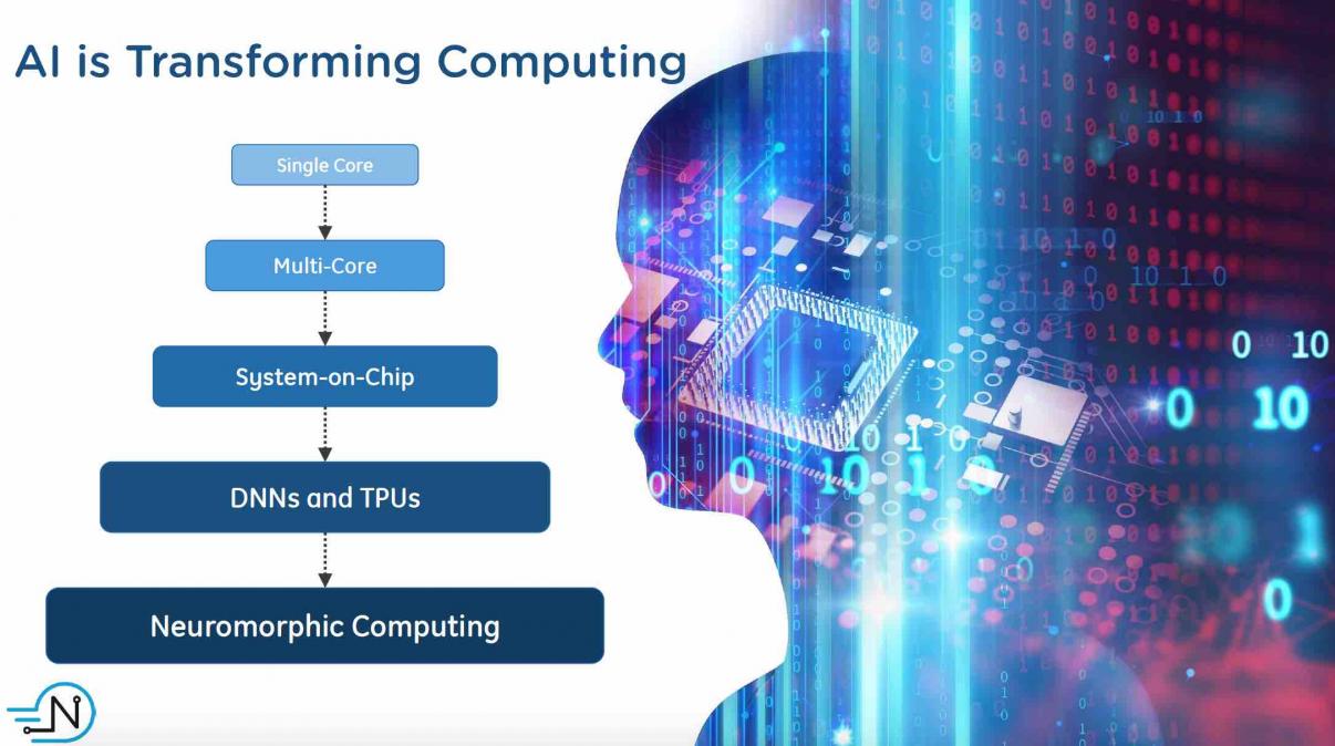
Bronco Webinar 800x100 1

More Than Your Average IP Development Kit

More Than Your Average IP Development Kit
by Bernard Murphy on 02-13-2018 at 7:00 am

When I think of an IP development kit, I imagine software plus a hardware model I can run on a prototyper or, closer to the kits offered by semi companies, software plus a board hosting an FPGA implementation of the IP along with DDR memory, flash and a variety of interfaces. These approaches work well for IP providers because hardware investment in both cases is relatively modest.

But neither of these solutions fits well for a kit supporting a high-speed IP. How do you effectively develop and test systems and software at GHz real-time speeds with a prototyping model running (best case) at 10’s of MHz or an FPGA implementation perhaps running (again best case) at 100MHz? The answer of course is that the implementation has to be an SoC.

This is exactly what Synopsys has built for their ARC HS development kit, which indeed will run at 1GHz. Of course the IC holds more than an ARC core. This is a full-featured SoC supporting up to quad-core HS3x configurations along with a Vivante GPU, and interfaces for DDR, SPI, I2C, WiFi/BT, Ethernet, USB, a variety of analog interfaces and more. The board itself hosts 4GB of DDR memory, 2MB of flash, EEPROM and SD card slot, WiFi/BT module and a variety of other slots, altogether making this a true high-performance and low-power single board computer.

Which is important because for a lot of the applications to which you might target ARC HS, you want to be able to run Linux, also supported in the kit, so you can be up and running out of the box. That said, the kit supports a wide range of open source software from bare metal drivers and RTOSes to complete Linux distributions, which can be built with Buildroot and Yocto. The embARC Open Software Platform (OSP) supports the ARC HS Development Kit and includes drivers, FreeRTOS and middleware targeted at IoT and general embedded applications. Toolchain support is provided by the GNU Toolchain for ARC Processors and the MetaWare Development Toolkit (a commercial offering from Synopsys). All the open source software is available from the embARC.org web site.

Allen Watson, product marketing manager for software development tools for ARC, told me the kit is very extensible, providing headers for Arduino, Digilent Pmod and mikroBUS modules, also for fast AXI tunneling to Synopsys’ HAPS prototyper. Allen told me it is also very easy to connect sensors to the kit. All of which should enable you to quickly assemble a system in support of software development and product prototyping, while your hardware design team gets on with the more detailed SoC architecture.

Where is a solution like this going to help development? Allen mentioned WiFi routers, IoT gateways, higher-end storage (such as SSDs), baseband control, digital TV and home appliances, all areas where high performance demands are common but with an expectation of low power, the sweet spot for ARC HS.

There is also a lot of activity in this area around automotive support. I can’t find a customer reference, but Synopsys cite the value in power, performance and area of ARC HS processors for automotive applications and their MetaWare tool-chain is ASIL-D certified, a level I can’t believe Synopsys would have gone to if they weren’t working with someone (several someones if they’re following their usual path). And there’s this piece suggesting the ARC HS is particularly targeted for use in initiating and scheduling control of BIST in safety-critical systems.

I find a couple of things especially interesting about this announcement. First, Synopsys is providing a development kit on a level with those provided by semiconductor enterprises (and ARM), based on an SoC rather than an FPGA. I don’t think this is their first (I think they have a similar solution for IoT support), but it’s quite interesting that they now feel comfortable shipping Synopsys-designed SoCs in products. No threat to their customers of course – these are very narrow purpose-built devices. Still, this is a logical outcome to having all the tooling, most of the IP, foundry relationships and a lot of in-house design expertise.

The second point I find interesting is their accommodation for makers, particularly through Arduino and mikroBUS support, as well as more traditional big semi flows. Allen told me that this is quite deliberate. He sees an opportunity with those in the maker community who need high-performance, low-power computing as a part of their solution. This could be an interesting new market for Synopsys.

You can learn more about the ARC HS development kit HERE.


IEDM 2017 – Leti Gate-All-Around Stacked-Nanowires

IEDM 2017 – Leti Gate-All-Around Stacked-Nanowires
by Scotten Jones on 02-12-2018 at 12:00 pm

At IEDM in December I had a chance to interview Thomas Ernst about the paper “Performance and Design Considerations for Gate-All-around Stacked-NanoWires FETs” by Leti and STMicroelectonics.

Leti published the first stacked nanowire in 2006, it was very new then, now stacked nanowire/nanosheets are starting to show up in commercial roadmaps. IBM working with Samsung and GLOBALFOUNDRIES has published on 5nm nanosheets at VLSIT in 2017 and Samsung has announced a foundry roadmap including 4nm nanosheets they refer to as multi bridge channel due in 2020.

Logic designs are built using standard cells where the size of a standard cell depends on the contacted poly pitch (CPP), minimum metal pitch (MMP) and track height, see figure 1.

Figure 1. 7.5 track standard cell

In order to shrink standard cells, the industry has moved to design-technology-co-optimization (DTCO) where CPP, MMP and track height are all shrunk.

CPP is made up of three elements, gate length (L[SUB]G[/SUB]), spacer thickness (t[SUB]SP[/SUB]) and contact width (W[SUB]C[/SUB]), see figure 2.


Figure 2. Elements that make up contacted poly pitch.

Where CPP is given by:

CPP = L[SUB]G[/SUB] + 2t[SUB]SP[/SUB] + W[SUB]C[/SUB]

In order to maintain good electrostatic control, a FinFET with gates on 3 sides of the channel has a minimum L[SUB]G[/SUB] limit of around 16nm [1]. Gate-All-Around (GAA) adds a gate on the fourth side of the channel and improves electrostatic control enabling an L[SUB]G[/SUB] of approximately 13nm [1].

Another important consideration is how to achieve acceptable drive current at shrinking dimensions. Drive current is proportional to the effective channel width W[SUB]eff[/SUB]. One current trend in the industry is reducing track height that results in fin depopulation, for example a 7.5-track cell as shown in figure 1 has 3 fins for the nFET and 3 fins for the pFET, a 6-track cell as shown in figure 3, only has 2 fins for the nFET and 2 for the pFET. TSMC and GLOBALFOUNDRIES have both implement 6 track cells at 7nm. At the same fin height, the W[SUB]eff[/SUB] decreases as the number of fins is reduced.


Figure 3. 6 track standard cell

Simply changing from a FinFET to a stacked horizontal nanowire with 3 wire and the same width and height as the fin, results in improved electrostatics but also a 14% reduction in W[SUB]eff[/SUB]. The ideal would be to be able to combine GAA electrostatics with FinFET drive current.

If instead of nanowires you make nanosheets by varying the width of the sheet you can achieve greater W[SUB]eff[/SUB] than a FinFET, see figure 4.


Figure 4. Weff for nanowires, FinFET and nanosheets [2].

The effect of nanosheet width on short channel effects is shown in figure 5.


Figure 5. Short channel effects versus nanosheet width [2].

Between figure 4 and figure 5, you can see that nanosheets achieve better electrostatics and drive current than FinFETs. The ability to trade-off/tune drive current and electrostatics ultimately offers better overall power -performance and power-performance tuning than FinFETs, see figure 6.

Figure 6. Power/performance trade-off [2].

Leti has shown patterning of up to 13 nanosheet layers while maintaining a crystalline film. There may be a trade-off between number of layers and performance due to capacitance, this is an area still being explored.

Strain management is critical to nanosheet performance and inner spacers are required to minimize capacitance.

There is still work to be done on nanosheet/nanowire development but it is showing great promise for post FinFET scaling.

In conclusion, horizontal nanosheets are a promising replacement for FinFETs with better electrostatics and higher drive current.

References

[1] J.P. Colinge, p 313, SISPAD (2014).
[2] S. Barraud, V. Lapras, B. Previtali, M.P. Samson, J. Lacord, S. Martinie, M.-A. Jaud, S. Athanasiou, F. Triozon, O. Rozeau, J.M. Hartmann, C. Vizioz, C. Comboroure, F. Andrieu, J.C. Barbé, M. Vinet, and T. Ernst, ” Performance and Design Considerations for Gate-All-Around Stacked-NanoWires FETs.” p 677, IEDM (2017).


Qualcomm Continues to Mislead its Own Stockholders

Qualcomm Continues to Mislead its Own Stockholders
by Daniel Nenni on 02-12-2018 at 7:00 am

The war of words continues between Broadcom and Qualcomm and the stock analysts still seem to be split on the merger. Please note that Broadcom is proposing to merge with Qualcomm instead of a tender offer which is what Qualcomm has proposed for the acquisition on NXP. Same result but two very different approaches. Another interesting point is that the merger agreement as it is written today will all but kill the NXP acquisition.

January 3[SUP]rd[/SUP], 2018 Broadcom PR:Qualcomm has once again made intentionally vague statements regarding “regulatory challenges” that are simply unfounded, misleading, and a disservice to Qualcomm stockholders. Qualcomm’s rhetoric is vague for a reason – because it is not grounded in reality. While it appears that Qualcomm will say anything to remain a standalone company, here are the facts:


Last week Broadcom issued a press release which included the proposed merger agreement. I’m sure this was already shopped around to the large QCOM stockholders but for us common folks it had more detailed information to sway public opinion. Remember, this will be Hock’s 7[SUP]th[/SUP] acquisition in five years under the AVAGO brand so let’s all assume he might just know what he is doing.

Here are the press releases and presentations from Broadcom:

  • Press Release with Letter and Merger Agreement Read More
  • Broadcom Presents Best and Final Offer for Qualcomm Read More
  • Broadcom Comments on Qualcomm’s Statements Read More
  • Broadcom Presentation – Feb. 5, 2018 Read More
  • A Conversation with Antitrust Counsel to Broadcom Read More

We can chat more about this in the comment section. The Merger Agreement is 80+ pages long and well above my pay grade so I had a good friend, who specializes in such things, take a close look and explain it to me using small words. His personal opinion, and I agree 100%, is that Hock is a very clever man who is trying to brute force this acquisition and will most probably succeed. If you don’t agree, my friend says short QCOM because without this acquisition the stock is going to get a serious haircut (15-20% drop), his words not mine.

The one thing that my friend did not know is how the semiconductor industry got to where it is today and where it is going tomorrow. The story I offered him (which is documented in our book “Fabless: The Transformation of the Semiconductor Industry”) started with the transformation of the semiconductor industry from IDMs “Real men have fabs” to the fabless model made possible by pure-play foundries (TSMC) and fabless chip companies (QCOM, NVDA, AVGO, etc…) that now dominate the $400B+ semiconductor industry.

The next transformation, the one that is currently taking place, is the transformation from fabless chip companies to fabless system companies such as Apple, Huawei, Samsung, Tesla, Amazon, and many MANY others. Consolidation amongst the fabless semiconductor companies has been fierce the past three years and that will continue as the fabless systems company transformation gains momentum.

We have a front row seat to this transformation on SemiWiki.com since we see which domains are reading which articles and can sort the analytics in dozens of different ways (company, market segment, topic, etc…). Fabless systems companies have dominated SemiWiki readership for the past three years and that trend is growing, absolutely.

My good friend then asked: Why would a systems company spend the money to build a chip they can buy? I presented him with a handful of reasons but the one that resonated with him the clearest is the FPGA Prototyping / Emulation case study. By using FPGA prototyping and emulation platforms, systems companies can start software development well before a chip is taped-out much less delivered which is a serious competitive advantage in regards to time-to-market as well as the ability to customize the chip for the software and vice versa.

Broadcom and Qualcomm will meet on Valentine’s Day to discuss the proposed merger agreement so we will no doubt hear more shortly thereafter from anonymous sources close to the discussions…. ❤️

Bottom line:
QCOM stock is headed for the tar pits without a sharp penciled businessman like Hock Tan at the helm, my opinion.

Also read:

Broadcom versus Qualcomm Update

Broadcom buying Qualcomm just won’t happen? (Poll)


Quantum computers may be more of an imminent threat than AI

Quantum computers may be more of an imminent threat than AI
by Vivek Wadhwa on 02-11-2018 at 7:00 am

Elon Musk, Stephen Hawking and others have been warning about runway artificial intelligence, but there may be a more imminent threat: quantum computing. It could pose a greater burden on businesses than the Y2K computer bug did toward the end of the ’90s.

Quantum computers are straight out of science fiction. Take the “traveling salesman problem,” where a salesperson has to visit a specific set of cities, each only once, and return to the first city by the most efficient route possible. As the number of cities increases, the problem becomes exponentially complex. It would take a laptop computer 1,000 years to compute the most efficient route between 22 cities, for example. A quantum computer could do this within minutes, possibly seconds.

Unlike classic computers, in which information is represented in 0’s and 1’s, quantum computers rely on particles called quantum bits, or qubits. These can hold a value of 0 or 1 or both values at the same time — a superposition denoted as “0+1.” They solve problems by laying out all of the possibilities simultaneously and measuring the results. It’s equivalent to opening a combination lock by trying every possible number and sequence simultaneously.

Albert Einstein was so skeptical about entanglement, one of the other principles of quantum mechanics, that he called it “spooky action at a distance” and said it was not possible. “God does not play dice with the universe,” he argued. But, as Hawkings later wrote, God may have “a few tricks up his sleeve.”

Crazy as it may seem, IBM, Google, Microsoft and Intel say that they are getting close to making quantum computers work. IBM is already offering early versions of quantum computing as a cloud service to select clients. There is a global race between technology companies, defense contractors, universities and governments to build advanced versions that hold the promise of solving some of the greatest mysteries of the universe — and enable the cracking open of practically every secured database in the world.

Modern-day security systems are protected with a standard encryption algorithm called RSA (named after Ron Rivest, Adi Shamir and Leonard Adleman, the inventors). It works by finding prime factors of very large numbers, a puzzle that needs to be solved. It is easy to reduce a small number such as 15 to its prime factors (3 x 5), but factorizing numbers with a few hundred digits is extremely hard and could take days or months using conventional computers. But some quantum computers are working on these calculations too, according to IEEE Spectrum. Quantum computers could one day effectively provide a skeleton key to confidential communications, bank accounts and password databases.

Imagine the strategic disadvantage nations would find have if their rivals were the first to build these. Those possessing the technology would be able to open every nation’s digital locks.

We don’t know how much progress governments have made, but in May 2016, IBM surprised the world with an announcement that it was making available a 5-qubit quantum computer on which researchers could run algorithms and experiments. It envisioned that quantum processors of 50 to 100 qubits would be possible in the next decade. The simultaneous computing capacity of a quantum computer increases exponentially with the number of qubits available to it, so a 50-qubit computer would exceed the capability of the top supercomputers in the world, giving it what researchers call “quantum supremacy.”

IBM delivered another surprise 18 months later with an announcement that it was upgrading the publicly available processor to 20 qubits — and it had succeeded in building an operational prototype of a 50-qubit processor, which would give it quantum supremacy. If IBM gets this one working reliably and doubles the number of qubits even once more, the resultant computing speed will increase, giving the company — and any other players with similar capacity — incredible powers.

Yes, a lot of good will come from this, in better weather forecasting, financial analysis, logistical planning, the search for Earth-like planets, and drug discovery. But it could also open up a Pandora’s box for security. I don’t know of any company or government that is prepared for it; all should build defenses, though. They need to upgrade all computer systems that use RSA encryption — just like they upgraded them for the Y2K bug.

Security researcher Anish Mohammed says that there is substantial progress in the development of algorithms that are “quantum safe.” One promising field is matrix multiplication, which takes advantage of the techniques that allow quantum computers to be able to analyze so much information. Another effort involves developing code-based signature schemes, which do not rely on factorizing, as the common public key cryptography systems do; instead, code-based signatures rely upon extremely difficult problems in coding theory. So the technical solutions are at hand.

But the big challenge will be in transitioning today’s systems to a “post-quantum” world. The Y2K bug took years to remediate and created fear and havoc in the technology sector. For that, though, we knew what the deadline was. Here, there is no telling whether it will take five years or 10, or whether companies will announce a more advanced milestone just 18 months from now. Worse still, the winner may just remain silent and harvest all the information available.

For more, you can read my book, The Driver in the Driverless Car: How Our Technology Choices Will Create the Future


Design Automation Conference Silicon and Technology Art Show

Design Automation Conference Silicon and Technology Art Show
by Daniel Nenni on 02-09-2018 at 7:00 am

This year the 55th annual Design Automation Conference is in San Francisco and the Silicon and Technology Art Show, one of my favorite DAC events, is back! Favorite because it’s something my beautiful wife and I can share. She is very artistic and has an eye for colors and I actually know what the art is so we make a good team. I am a judge again this year (with the help of my wife) but we need submissions to fill out the categories and that is where you come in. If you see the beauty in your work please share it at #55DAC! This is last year’s winner “14nm FinFET Technology by Coventor”.

DAC Silicon/Technology Art Show
At DAC, we want to showcase the beauty of our work for the rest of the world to see. That’s why we are hosting the Silicon/Technology Art Show for the second time at DAC this year, and we want you to participate by submitting your digital images.

Submission Deadline April 15, 2018

Examples of what we are looking for include but not limited to:

  • Die photoshots of silicon designs. These are the end product of hard EDA and design work, and often the result is breathtaking.
  • Design floorplans and placements, especially if they are illustrated in such a way to show interest.
  • 3D wiring or clock tree visualizations.
  • Lithographic images.
  • Thermal maps, congestion maps, interesting logic structures, or just about anything you can think of related to EDA and Semiconductor.
  • Submitted work can be either hardware design images or software design images.
  • We cannot accept movies, but you may submit a sequence of images (e.g., 6) that can be framed to show how an algorithm works.

This is your chance to have the work you (and or your company) produces to be recognized.

Each piece submitted will be printed on canvas and displayed at the Art Show starting on Monday, June 25, 2018 at Moscone Center West. Judges will have an opportunity to review the displayed pieces and winners for each category will be announced Monday night at the Art Show reception.

Pieces will be judged in several categories:
Best visualization
Most inspiring
Most insightful
Most artistic
Grand Prize – Best piece out of all categories

Winners in each category will receive a trophy for recognition and will also be on the cover of IEEE Design & Test magazine. Click the links below to see past covers.

IEEE Design & Test – January/February 2017 Cover
IEEE Design & Test – November/December 2016 Cover

DAC will handle the printing and coordinate the displays. All of those who submit artwork that is used in the art show are welcome to take the final piece home with them.

This is my 34th DAC and while I enjoy having it close to home I am really looking forward to next year’s venue which is Las Vegas. My second DAC was in Las Vegas in 1985 and it was the first DAC my wife attended. I remember her being a little shocked at how wild the parties were but we were newlyweds and had a great time. The EDA industry has matured now and the parties are much more sedate, but then so are my wife and I. It should be full of reminiscing and fun, absolutely!


Webinar: Multiphysics Reliability Signoff for Next-Generation Automotive Electronics Systems

Webinar: Multiphysics Reliability Signoff for Next-Generation Automotive Electronics Systems
by Bernard Murphy on 02-08-2018 at 7:00 am

In case you missed the TSMC event, ANSYS and TSMC are going to reprise a very important topic – signing-off reliability for ADAS and semi-autonomous /autonomous systems. This topic hasn’t had a lot of media attention amid the glamor and glitz of what might be possible in driverless cars. But it now seems like the cold light of real engineering needs are advancing over the hype, if this year’s CES is any indication (see my previous blog on CES). Part of that engineering reality is ensuring not only that we can build these clever systems but that they will also continue to work for a respectable amount of time; in other words that they will be reliable, a topic as relevant for today’s advanced automotive electronics as it is for the systems of tomorrow.

REGISTER HERE for this event on February 22nd at 8am Pacific Time

This topic is becoming a pressing concern, especially for FinFET-based designs. There are multiple issues impacting aging, stress and other factors. Just one root-cause should by now be well-known – the self-heating problem in FinFET devices. In planar devices, heat generated inside a transistor can escape largely through the substrate. But in a FinFET, dielectric is wrapped around the fin structure and, since dielectrics generally are poor thermal conductors, heat can’t as easily escape leading to a local temperature increase, and will ultimately escape significantly through local interconnect leading to additional heating in that interconnect. Add to that increased Joule heating thanks to higher drive and thinner interconnect and you can see why reliability becomes important.

ANSYS has developed an amazingly comprehensive range of solutions for design for reliability, spanning thermal, EM, ESD, EMC, stress and aging concerns. In building solutions like this, they work very closely with TSMC, so much so that they got three partner of the year awards at the most recent TSMC OIP conference!

Incidentally my CES-related blog is here: https://www.legacy.semiwiki.com/forum/content/7274-ces-exhibitor-s-takeaway.html

Summary
Design for reliability is a key consideration for the successful use of next-generation systems-on-chip (SoCs) in ADAS, infotainment and other critical automotive electronics systems. The SoCs manufactured with TSMC’s 16FFC process are advanced multicore designs with significantly higher levels of integration, functionality and operating speed. These SoCs must meet the rigorous requirements for automotive electronics functional safety and reliability.

Working together, ANSYS and TSMC have defined workflows that enable electromigration, thermal and ESD verification and signoff across the design chain (IP to SoC to package to system). Within the comprehensive workflows, multiphysics simulations capture the various failure mechanisms and provide signoff confidence not only to guarantee first-time product success, but also to ensure regulatory compliance.

Attend this ANSYS and TSMC webinar to learn about ANSYS’ chip-package-system reliability signoff solutions for creating robust and reliable electronics systems for next-generation automotive applications, and to explore case studies based on TSMC’s N16FFC technology.

Founded in 1970, ANSYS employs nearly 3,000 professionals, many of whom are expert M.S. and Ph.D.-level engineers in finite element analysis, computational fluid dynamics, electronics, semiconductors, embedded software and design optimization. Our exceptional staff is passionate about pushing the limits of world-class simulation technology so our customers can turn their design concepts into successful, innovative products faster and at lower cost. As a measure of our success in attaining these goals, ANSYS has been recognized as one of the world’s most innovative companies by prestigious publications such as Bloomberg Businessweek and FORTUNE magazines.

For more information, view the ANSYS corporate brochure.


Machine Learning And Design Into 2018 – A Quick Recap

Machine Learning And Design Into 2018 – A Quick Recap
by Alex Tan on 02-07-2018 at 3:00 pm

How could we differentiate between deep learning and machine learning as there are many ways of describing them? A simple definition of these software terms can be found here. Let’s look into Artificial Intelligence (AI), which was coined back in 1956. The term AI can be defined as human intelligence exhibited by machines. While machine learning is an approach to achieve AI and deep learning is a technique for implementing subset of machine learning.


During last year 30-Year Anniversary of TSMC Forum, nVidia CEO Jen-Hsen Huang mentioned two concurrent dynamics disrupting the computer industry today, i.e.,how software development is done by means of deep learning and how computing is done through the more adoption of GPU as replacement to single-threaded/multi-core CPU, which is no longer scale and satisfy the current increased computing needs. The following charts illustrate his message.


At this month Santa Clara DesignCon2018 there were multiple well-attended sessions (2 panels and 1workshop) addressing Machine Learning Advances in Electronic Design. Highlighted by panelists coming from 3 different areas (EDA, industry and academia) were some successful snapshots of ML application in optimizing design and its potential consequences as how we should handle the generated models and methodologies.

From the industry:
Chris Cheng, a Distinguished Engineer from HPE presented a more holistic view of ML potential use coupled with test instruments as substitute for a software model based channel analysis. He also projected ML use to perform more proactive failure prediction of signal buses or complicated hardware such as solid-state drives.


Ken Wu, Google Staff HW Engineer shared his works on applying ML in channel modeling. He proposed the use of ML to predict channel’s eye-diagram metrics for signal integrity analysis. The learned models can be used to circumvent the need of performing complex and expensive circuit simulations. He believes ML opens an array of opportunity for channel modeling such as extending it to analyze the four-level pulse amplitude modulation (PAM-4) signaling, and the use of Deep Neural Network for Design of Experiment (DOE).

Dale Becker, IBM Chief Engineer of Electronic Packaging Integration, alluded to the potential dilemma imposed by ML. Does it supersede today’s circuit/channel simulation techniques, or is it synergistic? With the current design methodologies still reflecting heavy human interventions (such as in channel diagnostics, evaluation, optimization, physical implementation), ML presents an opportunity for exploration. On the other side of the equation, we need to be ready to address standardization, information sharing and IP protection.

From the EDA world, both Synopsys and Cadence were represented:

Cadence team — David White (Sr. Group Director), Kumar Keshavan (Sr. Software Architect) and Ken Willis (Product Engineering Architect) highlighted Cadence contribution in advancing ML adoption. David shared what Cadence has achieved with ML over the years on Virtuoso product and raised the crucial challenge of productizing ML. For a more in-depth coverage for David’s similar presentation on ML, please refer to another Wiki article TSMC EDA 2.0 With Machine Learning – Are We There Yet ? Kumar delved into Artificial Neural Network (ANN) concept and suggested its application for DOE of LPDDR4 bus. Ken Willis was moderating the afternoon panel and highlighted the recently introduced IBIS ML versus AMI model as well as impact of ML on solution space analysis.


Sashi Obilisetty, Synopsys R&D Director pointed out that the EDA ecosystem comprising of academic research, technology availability and industry interest) is ready and engaged. What we need is a robust, scalable, hi-performance and near real time data platform for ML application.

Several academia also shared their research progress under the auspice of Center for Advanced Electronics Through Machine Learning (CAEML) since its formation in 2016:

Prof. PaulFranzon discussed how ML could shorten IC physical design step through the use of surrogate model. The concept is to train a fast global model to evaluate from multiple evaluations of a detailed model that is slow to evaluate. Given an SOC design requiring a 40 minute per route iteration, the team needs about 50 runs to complete the Kriging based model overnight. Using this model, an optimal design can be obtained in 4 iterations which otherwise requires 20 iterations. The design has 18K gates derived from Cortex-M0 with 10ns cycle time and 45nm generic process.

Prof. Madhavan Swaminathan presented another application of ML based solution using surrogate model on channel performance simulation.

His view: Engineer (thinker) + ML (enabler) + Computers (doers) = enhanced solution. Extending ML into design optimization through active learning may ensure convergence to global optima and minimizing required CPU time.

With the increased design activities and research efforts in ML/DL applications, we should anticipate more coverage of such implementation into 2018. The next question would be if it will create a synergy and enhance design efforts through retooling and methodology adjustments, or it will create disruption that may change the human designer roles at different junctures of design capture. We should see.


High Performance Ecosystem for 14nm-FinFET ASICs with 2.5D Integrated HBM2 Memory

High Performance Ecosystem for 14nm-FinFET ASICs with 2.5D Integrated HBM2 Memory
by Mitch Heins on 02-07-2018 at 10:00 am


High Bandwidth Memory (HBM) systems have been successfully used for some time now in the network switching and high-performance computing (HPC) spaces. Now, adding fuel to the HBM fire, there is another market that shares similar system requirements as HPC and that is Artificial Intelligence (AI), especially AI systems doing real-time image recognition. I traded notes with Mike Gianfagna at eSilicon to get more information and he pointed me to a webinar that eSilicon had recently presented (link below) in conjunction with Samsung, Rambus, Northwest Logic and the ASE group.

I reviewed the webinar recordings to which Mike had referred me and learned a great deal more about HBM-based systems. According to Lisa Minwell of eSilicon, both networking and AI applications typically have large ASIC die, greater than 400mm[SUP]2[/SUP], containing high-performance cores, up to 1 gigabit of configurable multi-port embedded memories, and high-bandwidth wide-word interfaces to HBM2 stacked memories all integrated in a 2.5D system-in-a-package (SiP).

These SiPs use cutting-edge technology and as a result are complex and require an ecosystem of partners to ensure successful design, implementation and test. And that, as it turns out, was exactly what the webinar was about.

The webinar had a ridiculously long title, something like “FinFET ASICs for Networking, Data Center, AI, and 5G using 14nm 2.5D HBM2 and SERDES”. I think that was more for Google search engines – and so I include it here as well. True to form though, the webinar did in fact cover all those topics and at pretty good depth, much more than I can summarize here. As mentioned, the webinar included panelists from the companies listed above and covered the following areas:

  • HBM2 memories – Samsung Electronics
  • 14nm FinFET silicon – Samsung Foundry
  • 2.5D packaging, interposers assembly/test and micro-bump road maps – the ASE group
  • ASIC design services, configurable memory compilers and PHY IP – eSilicon
  • High-speed SERDES IP – Rambus
  • HBM2 memory controller IP – Northwest Logic

Each company gave a brief overview of their offerings along with road map data for their part in the overall solution. There was a ton of excellent data in the webinar that simply would not fit in this space. If you are interested in road map data for any of these areas, please make sure to follow the link below to watch the webinar. The recording is indexed by subject matter so that you can quickly go to the section of your interest.

One thing all the members made sure to point out was that this wasn’t “futures” work. The work they were doing with HBM2 was being used in real products with significant performance, power and area improvements for their customers. Note the ~2.5X improvement in overall system performance gained over DDR architectures when using HMB2. HBM3 (generation 3), due out sometime toward the end of the decade, is supposed to have 2X more performance than HBM2.


One of the interesting parts of this type of design is that you are dealing with multiple components from different companies. The tricky part of course is where to look when things don’t work as planned. This is where the eco-system partners were all quick to jump in and ensure their listeners that they were all there to work out any issues that come up. And… given their previous history of working with each other, the message was clear that they had figured out how to do this in an efficient manner.

The other thing that came across from the webinar is that none of the systems that were discussed were exactly alike. In fact, just the opposite was true. While they all shared common characteristics, each design had been customized in some way and it was evident that each of the eco-system partners were prepared to help their customer in this customization process, whether that meant changing the amount or speed of the HBM2 stack, customizing different memory mapping for the stack, creating unique multi-port embedded memories for the ASIC, customizing a set of SERDES or a creating a customized interposer.

And that, is what makes their joint solution so compelling. It is the ability to use and customize a design using production proven 14nm FinFET technology with silicon verified IP blocks that have been verified against each other. That’s hard to do when all the pieces are coming from different places. If you are doing networking, HPC or AI applications you may want to check out this webinar at the link below!

See Also: (in the order in which they presented)
Webinar Link
Samsung HBM2 website
Samsung Foundry website
the ASE Group website
eSilicon website
Rambus website
Northwest Logic website


Increased Processing Power Moves to Edge

Increased Processing Power Moves to Edge
by Tom Simon on 02-06-2018 at 12:00 pm

Recently there has been a lot of buzz about 5G networks. Aside from the talk about it possibly being nationalized, 5G will be a lot different than its predecessors. Rather than a single data link in a predetermined band, 5G will consist of a web of connections all working together to support existing types of data traffic and many new types, including automotive, IoT and others. In urban areas, there will be a large number of smaller nodes using GHz bands that do not travel far. Also, it will support IoT and automotive data traffic traffic that will require low latency and packet sizes suited to the data payloads.

Many of the effects of this shift in mobile data architecture are readily understandable, but there are other more subtle shifts in data communication and processing that are going to affect where compute resources are deployed. We live in the era of cloud computing. This is exemplified by light weight edge computing power augmented by heavy duty processing resources in the cloud. Many tasks manifest only as a user interface or have low compute requirements on edge devices, and the heavy lifting is done at data centers.

However, we are about to enter another cycle where the location of processing activity makes a significant migration. IoT and the automotive communications known as V2V (vehicle to vehicle) and V2X (vehicle to other) demand lower latency and more localized processing. A recent white paper by Achronix talks about these trends and the requirements they will impose on processing devices. The paper, “2018 Ushers in a Renewed Push to the Edge”, provides many specific examples of why edge processing demands will expand significantly.

Coming back to 5G, one of the new capabilities will be millisecond latency. Older networks have much higher latency and extended backhaul routing can add to huge delays to system responsiveness. In the case of moving vehicles dealing with their environment or other vehicles, time is of the essence. V2X is one of the more interesting topics. Roadside beacons can aggregate and communicate information about road surface conditions, traffic, obstacles, and other cars. V2V can be used to enhance safety to broadcast obscured hazard information.

Another harbinger of how computing is moving to the edge that is discussed in the Achronix white paper are services like Amazon Web Services’ Greengrass offering. Instead of requiring all network traffic to return to AWS for processing, Greengrass lets system designers define IoT based applications in the cloud and then instantiate them in remote/edge processing nodes that can operate without an active connection to AWS. An edge processing unit is used to network IoT devices to create a local IoT network. One example is in a hospital where there might be pulse, temperature and other sensors that can be linked together in a patient’s room to provide intelligent monitoring.

Greengrass uses Amazon’s flavor of FreeRTOS for the hub at the edge in the processing unit. When internet connections are available the edge processor can update the cloud, but it can operate on its own without the need for a cloud connection.

The drive to add processing power at the edge raises the question of what is the best hardware design for achieving reliability, power, security and performance goals. We have seen, through Microsoft’s Catapult project, how marrying traditional CPU’s and programmable logic can boost server performance. Achronix asserts that the same benefits accrue at the edge. Programmable logic can be uniquely tailored to the specific edge processing needs. FPGA based packet and data processing can occur in parallel with low overhead for a range of tasks. If we look at security needs, because these edge nodes may not reside in physically secure facilities, they need to be fundamentally more secure. Embedded FPGA fabric admittedly is more secure and reduces power. Also, lower part count and reduced board interconnect can lead to better reliability. Achronix makes a convincing case that for many applications that require enhanced edge processing, that their embedded eFPGA fabric is a desirable solution. You should download the paper if you are interested in learning about the other motivations for increased edge processing power, and also to learn about how effective solutions can be architected.


CES: An Exhibitor’s Takeaway

CES: An Exhibitor’s Takeaway
by Bernard Murphy on 02-06-2018 at 7:00 am

There are few tech promises these days as prominent as those surrounding driverless cars (trucks, buses, …). But thanks to always-on media amplifiers, it’s not always easy to separate potential from reality. I recently talked to Kurt Shuler, VP Marketing at Arteris, who shared his view after returning from this year’s CES. Kurt is much an enthusiast as anyone but pointed immediately to the Gartner media-hype curve, saying that pitches were more muted this year, particularly in moving away from live demos, perhaps thanks to last year’s less than stellar performances. On the hype curve, Kurt feels we’ve moved past peak hype and are now into the long slog of delivery.

He’s not alone in this view. Others are also digging into the details, looking more closely at what it takes to get to different levels of autonomy and are more skeptical that wide-scale autonomy is right around the corner. No-one is saying it’s not going to happen, but reality is setting in on how long it’s going to take. In Kurt’s view, we’re 80% of the way there, but the last 20% is going to take years, maybe even decades.

Which obviously contrasts with the marketing message, since no-one wants to signal that they’re intentionally stretching out plans. Intel are making a big push with their acquisition of Mobileye, however a lot of what they are doing is immediately relevant to ADAS, whether or not autonomy takes longer. Tier1 companies are following a variety of strategies, some building their own systems (HW+SW), others using commercial branded systems under the hood and Baidu, Google Waymo push their big data mining/management advantage, though still unclear to me how far Google will get, given their spotty record on Other Bets.

Among OEMs, there’s a wide spectrum, from Tesla who always market to the hilt and seem to want to boil the ocean as fast as possible (witness now autonomous trucks), to perhaps Volvo who initially said they would offer autonomy in 2020 and now have pulled back, focusing more on driver assistance.

Obviously that last 20% represents the difference between what is possible and what is functionally safe, reliable and cost-effective, as in we’re prepared to let these things on the road in the real world and we can afford them. In our neck of the woods in semiconductor design, solution providers are still working hard to push into products more functionality with the “right” HW/SW and PPA balance. What makes for right depends on perspective. The Tier1s are pushing for more to be done in hardware, especially when integrating their IP, and less in software since that means less software problems to manage in the field, a less complex software BOM and generally a reduced safety/security problem around that software.

This naturally requires jamming more functions into a system on chip. Mobileye is adding more hardware accelerators to the bus and Kurt said that NVIDIA is now adding fixed-point accelerators in their latest architecture. The NVIDIA move shouldn’t be surprising. While they dominate in neural net (NN) training, that’s running in the cloud where power isn’t such a big issue and the MAC instructions central to NNs can use floating-point accelerators. In a car, power is very much an issue, which is why NNs on edge applications (inferencing rather than training) have moved to more power-efficient fixed-point accelerators.

Still on the subject of power, functional safety tends to increase power since it requires levels of redundancy. A common method to mitigate the impact of hardware failures in a CPU (through soft errors for example) is to have two (or more) CPUs doing the same calculations, then compare the results. In other areas, duplication or triplication of logic is common in safety-critical functions. Good for safety, not so good for power.

And while on safety, naturally this demands a very high quality of service, even though there are all these units hanging off the bus, along with traffic from the growing number of sensors around the car. Kurt made the point that when you’re traveling at 70 mph and someone cuts in front of you, that clever electronics has milliseconds to respond; cars don’t stop on a dime. Rolling that back into the system, functions on the bus have to be responding at picosecond levels – reliably, not “most of the time unless bus traffic gets heavy”. This takes very careful optimization and a bus architecture which can support that optimization; I’m pretty sure everyone would agree this has to be a NoC .

One more point on safety. When functionality is divided up between multiple components provided by multiple suppliers and assembled by a solution builder, how does the system builder ensure overall system safety? Through redundancy certainly, but how do they deal with varying or differing levels of safety management between these functions? More responsibility for safety management probably has to fall on or at least be mediated by the interconnect.

Looks like there’s still a lot of hard work to be done to turn autonomy promise into a scalable reality but that shouldn’t be a big surprise. Meantime on-chip interconnect, particularly NoC interconnect, is likely to play a significant role in those solutions. You can learn more about Arteris solutions HERE.