Intento Design builds responsive analog EDA. The ID-Xplore tool is used for analog design acceleration and technology porting at the functional level, helping companies move analog IP quickly between technology nodes and across business units. The Intention view is a simple, elegant, and powerful concept that gives the speed of digital design to the analog designer for the first time. Intento Design receives a lot of questions on how the Intention view was conceived and how it works.
The following is a Q&A discussion with Dr. Caitlin Brandon of Intento Design:
How did Intento Design create the Intention view?Well, Analog EDA has proven very difficult for many reasons but mostly because the approach used by analog designers was not considered. From their training, analog designers are much more pen-and-paper than digital designers and these processes are counterintuitive to automate.
For instance, the first training an analog designer receives is usually the DC bias of an amplifier. The DC bias and sizing are calculated with pen-and-paper, transistor size data is entered in the schematic by hand and an AC performance simulation is started with a SPICE simulator. Performance results from the hand-calculated DC bias calculation are now seen for the first time. Clearly, using a pen-and-paper approach, getting to the performance results is slow.
But, here’s the interesting thing, before starting an AC analysis, the SPICE simulator first calculates the DC operating point using a DC solver. Likewise, a TRAN analysis also requires the starting DC operating point calculation, with energy stored in components. For Periodic AC, a more complex analysis necessary for modern mixed-signal analog systems, multiple DC operating points are calculated using – you guessed it – the DC solver. Spot the trend? Yes – SPICE simulation relies on the DC solver.
There it is – if a designer could directly choose their optimal DC operating point, the AC, TRAN and other performances would be met in an almost straightforward manner. The importance of DC analysis has been underestimated in analog design automation. And the EDA industry has failed to provide a tool for design of the analog circuit DC bias – until now.
So, the Intention view is used for DC bias and transistor size calculations? Yes, ID-Xplore uses the testbench directly for performance analysis, and the innovation of the Intention view provides the ability to quickly calculate transistor size data.
In creating the Intention view, it became really clear that the DC bias itself is not a simple act to follow. During calculation of a DC bias, the analog designer uses substantial explicit/trained knowledge and implicit/gained knowledge. Their trained knowledge obviously involves applied circuit analysis, such as Kirchhoff laws and known circuit topologies, whereas their gained knowledge may involve knowing by experience where signal frequency content will be lost due to the physical implementation. The designer understands – at a glance of the schematic – how analog sub-blocks work together to achieve block-level performance. To calculate a good DC operating point, the analog designer translates sub-block DC bias parameters into a first order model of some performance objectives and then calculates preliminary transistor sizing. It is this unique combination of advanced trained knowledge and advanced gained knowledge that makes analog circuit design challenging.
So – if it isn’t broke, why fix it?
Exactly. The analog designer knows how to describe their DC bias. What they really need is an automation tool to help them explore a range of bias and sizing in a technology PDK. Intento Design responded to this analog automation gap with the ID-Xplore tool and the Intention view.
What is the Intention view?
The Intention view is a text-based description of the analog circuit DC bias, written in a way which is very similar to the paper-and-pen version. The Intention view itself is technology independent, and an exploration can be done in any PDK. Electrical and physical parameters described in the DC bias, such as channel inversion, node voltage, branch current, transistor length – the list goes on – can be explored in just minutes to hours. With many varying parameters, the potential number of DC bias points can be quite large, often in the 100’s of millions, which obviously requires ID-Xplore automation to handle.
So, as a way of thinking about it, the Intention view is old-school – just like the pen-and-paper approach – and the ID-Xplore tool is new-school, advanced, automation enabling large scale exploration of the designer intentions (the Intention view).
But what happens to the performance specifications? As a plugin tool, the testbench performance specifications are evaluated at full SPICE accuracy for each individual DC bias point. Transistor sizing, previously handcrafted into transistor parameter fields in traditional design, is now fully automated. The ID-Xplore tool uses the OpenAccess database to back-annotate the designer selected DC bias and transistor sizing.
Does the Intention view play well with others – for collaboration? Yes, because collaboration and individual member experience are among the strongest factors impacting analog design team performance, the Intention view and ID-Xplore enable both knowledge transfer and training. Engineers share Intention views directly when they share the schematic database. For training, the ID-Xplore tool is useful to understand circuit sensitivity and design impacts at the performance level of the PDK. Exploration can uncover trends or verify hard limits of performance, illustrating where to concentrate design effort or when it is necessary to implement an entirely different schematic topology.
In short, the Intention view was created to allow designers to design, document and share a vision for the analog circuit performance as they see it – transistor by transistor.
Is Intention-based exploration faster than size-based optimizers?
Yes. Analog designers are plenty smart. At Intento Design, we like to think we are plenty smart too – for designing EDA tools. Here’s why.
Size-based optimizers use the SPICE DC solver on the whole circuit – even when only minor incremental or local size changes are required, resulting in substantial excess calculation. In addition, being size-based, the exploration requires many steps and can sometimes produce non-realizable results.
For ID-Xplore, we took a different approach. Using graph-theory, we analyzed the nodes and edges of the DC solver matrix and created a structural approach. While graph-theory itself can be very complex, the simple fact is that the number of SPICE calculations is much, much lower. In addition, variation of electrical parameters, rather than size, ensures that an exploration stays within a designer-validated region.
Analog designers appreciate right away the graph-based structural approach. Structural, of course, refers to the fact that the arrangement of the transistors in the circuit is taken in account while calculating size and bias. For instance, take a differential pair with a varying tail bias current. Assuming the input gate-voltage is fixed, the differential pair source-voltage varies with the current. Consequentially, changes can occur in the tail current transistor drain-voltage and the differential pair bulk-source voltage. Graph theory allows ID-Xplore sizing operations to accurately transmit branch-level, or even circuit-wide, information so local transistor sizing is correct-by-construction, taking into account both gross changes (current) as well as local effects, such as threshold voltage variation. When you think about it, this is exactly what the analog design engineer does with pen-and-paper.
So, the pen-and-paper approach of the analog designer really is best?Yes, that’s true, compared with a size-based optimizer, which is a brute force approach, the pen-and-paper approach is already more intelligent. The Intention view, combined with the exploration capabilities and data analytics of ID-Xplore, are designed to mirror quite closely the applied training of the analog designer. This means corporate investment in analog design team knowledge is not lost – but accelerated.
How does the Intention view enable technology porting?This is simple to understand. The Intention view is a parameterized description of the DC bias. And, while default values may be set inside the Intention view, it’s really inside the ID-Xplore tool that values are assigned for exploration in any given PDK. To move from one technology to another, the ID-Xplore tool is simply pointed at another technology PDK and the default parameters are adjusted for the exploration.
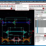
What tool is used to create the Intention view?The Intention view is created inside the Constraint Editor[SUP]TM[/SUP] of Cadence. To do this, a transistor or group of transistors is selected and then the Intento Design pull-down menu in the Constraint Manager tab is selected which opens the constraint entry field. The constraint data fields take parameterized electrical descriptions of the DC bias parameters, such as bias current and overdrive voltage. Once complete, the Intention view is exported to the ID-Xplore tool for design exploration using testbenches already setup in ADE-XL or ADE Assembler.
Figure 1 Creation of the Intention view inside the Constraint Editor of Cadence
Can you show an example of an ID-Xplore Intention view exploration?Yes, the following image shows design curve results in ID-Xplore. Each curve shows specifications that resulted from a unique DC bias point; the design curves together show the range of performances for the number of design points simulated. Selecting a specific solution shows the electrical values in the design point, the performances, and transistor size data. In this way the ID-Xplore tool really displays DC bias vs. performance, and size data is directly available for back-annotation.
Figure 2 ID-Xplore showing results of exploration of Intention view
How fast is Intention-based exploration using ID-Xplore?
Fast. Moving into 2018, Intento Design has worked on enhanced data display and faster operations to produce almost 200x speed performance under-the-hood of ID-Xplore. With multi-core parallel partitioning and advanced graph analysis, exploration on the DC bias of a multi-stage, fully-differential 75 transistor CMOS amplifier now takes only a few minutes.
Figure 3 Design acceleration using ID-Xplore
Minutes?
Well, the creation of the Intention view itself can take an hour or more, because this is really the analog hand-crafting aspect of the tool, but the exploration takes only minutes – yes. And, once created, the Intention view stays attached to the schematic to enable more exploration or technology porting. We believe ID-Xplore using the Intention view is an elegant, powerful and disruptive analog EDA – putting the speed of digital design into the analog designer’s hands for the first time.
Related Blog