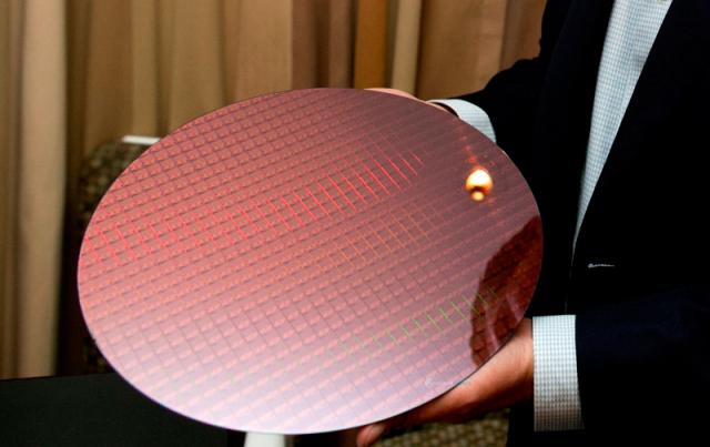
Bronco Webinar 800x100 1

First Line of Defense for Cybersecurity: AI

First Line of Defense for Cybersecurity: AI
by Ahmed Banafa on 02-25-2018 at 7:00 am

The year 2017 wasn’t a great year for cyber-security; we saw a large number of high-profile cyber attacks; including Uber, Deloitte, Equifax and the now infamous WannaCry ransomware attack, and 2018 started with a bang too with the hackingof Winter Olympics. The frightening truth about increasingly cyber-attacks is that most businesses and the cybersecurity industry itself are not prepared. Despite the constant flow of security updates and patches, the number of attacks continues to rise.

Beyond the lack of preparedness on the business level, the cybersecurity workforce itself is also having an incredibly hard time keeping up with demand. By 2021, there are estimated to be an astounding 3.5 million unfilled cybersecurity positions worldwide, the current staff is overworked with an average of 52 hours a week, not an ideal situation to keep up with non-stop threats.

Given the state of cybersecurity today, the implementation of AI systems into the mix can serve as a real turning point. New AI algorithms use Machine Learning (ML) to adapt over time, and make it easier to respond to cybersecurity risks. However, new generations of malware and cyber-attacks can be difficult to detect with conventional cybersecurity protocols. They evolve over time, so more dynamic approaches are necessary.

Another great benefit of AI systems in cybersecurity is that they will free up an enormous amount of time for tech employees. Another way AI systems can help is by categorizing attacks based on threat level. While there’s still a fair amount of work to be done here, but when machine learning principles are incorporated into your systems, they can actually adapt over time, giving you a dynamic edge over cyber criminals.

Unfortunately, there will always be limits of #AI, and human-machine teams will be the key to solving increasingly complex #cybersecurity challenges. But as our models become effective at detecting threats, bad actors will look for ways to confuse the models. It’s a field called adversarial machine learning, or adversarial AI. Bad actors will study how the underlying models work and work to either confuse the models — what experts call poisoning the models, or machine learning poisoning (MLP) – or focus on a wide range of evasion techniques, essentially looking for ways they can circumvent the models.

Four Fundamental Security Practices
With all the hype surrounding AI we tend to overlook a very important fact. The best defense against a potential AI cyber-attack is rooted in maintaining a fundamental security posture that incorporates continuous monitoring, user education, diligent patch management and basic configuration controls to address vulnerabilities. All explained below:

Identifying the Patterns
AI is all about patterns. Hackers, for example, look for patterns in server and firewall configurations, use of outdated operating systems, user actions and response tactics and more. These patterns give them information about network vulnerabilities they can exploit.

Network administrators also look for patterns. In addition to scanning for patterns in the way hackers attempt intrusions, they are trying to identify potential anomalies like spikes in network traffic, irregular types of network traffic, unauthorized user logins and other red flags.

By collecting data and monitoring the state of their network under normal operating conditions, administrators can set up their systems to automatically detect when something unusual takes place — a suspicious network login, for example, or access through a known bad IP. This fundamental security approach has worked extraordinarily well in preventing more traditional types of attacks, such as malware or phishing. It can also be used very effectively in deterring AI-enabled threats.

Educating the Users
An organization could have the best monitoring systems in the world, but the work they do can all be undermined by a single employee clicking on the wrong email. Social engineering continues to be a large security challenge for businesses because workers easily can be tricked into clicking on suspicious attachments, emails and links. Employees are considered by many as the weakest links in the security chain, as evidenced by a recent survey that found that careless and untrained insiders represented the top source of security threats.

Educating users on what not to do is just as important as putting security safeguards in place. Experts agree that routine user testing reinforces training. Agencies must also develop plans that require all employees to understand their individual roles in the battle for better security. And don’t forget a response and recovery plan, so everyone knows what to do and expect when a breach occurs. Test these plans for effectiveness. Don’t wait for an exploit to find a hole in the process.

Patching the Holes

Hackers know when a patch is released, and in addition to trying to find a way around that patch, they will not hesitate to test if an agency has implemented the fix. Not applying patches opens the door to potential attacks — and if the hacker is using AI, those attacks can come much faster and be even more insidious.

Checking Off the Controls

The Center for Internet Security (CIS) has issued a set of controls designed to provide agencies with a checklist for better security implementations. While there are 20 actions in total, implementing at least the top five — device inventories, software tracking, security configurations, vulnerability assessments and control of administrative privileges — can eliminate roughly 85 percent of an organization’s vulnerabilities. All of these practices — monitoring, user education, patch management and adherence to CIS controls — can help agencies fortify themselves against even the most sophisticated AI attacks.

Challenges Facing AI in Cybersecurity

AI-Powered Attacks
AI/Machine Learning (ML) software has the ability to “learn” from the consequences of past events in order to help predict and identify cybersecurity threats. According to a report by Webroot, AI is used by approximately 87% of US cybersecurity professionals. However, AI may prove to be a double-edged sword as 91% of security professionals are concerned that hackers will use AI to launch even more sophisticated cyber-attacks.

For example, AI can be used to automate the collection of certain information — perhaps relating to a specific organization — which may be sourced from support forums, code repositories, social media platforms and more. Additionally, AI may be able to assist hackers when it comes to cracking passwords by narrowing down the number of probable passwords based on geography, demographics and other such factors.

More Sandbox-Evading Malware

In recent years, sandboxing technology has become an increasingly popular method for detecting and preventing malware infections. However, cyber-criminals are finding more ways to evade this technology. For example, new strains of malware are able to recognize when they are inside a sandbox, and wait until they are outside the sandbox before executing the malicious code.

Ransomware and IoT
We should be very careful not to underestimate the potential damage IoT ransomware could cause. For example, hackers may choose to target critical systems such as power grids. Should the victim fail to the pay the ransom within a short period of time, the attackers may choose to shut down the grid. Alternatively, they may choose to target factory lines, smart cars and home appliances such as smart fridges, smart ovens and more.

This fear was realized with a massive distributed denial of service attack that crippled the servers of services like Twitter, NetFlix , NYTimes, and PayPal across the U.S. on October 21st , 2016. It’s the result of an immense assault that involved millions of Internet addresses and malicious software, according to Dyn, the prime victim of that attack. “One source of the traffic for the attacks was devices infected by the Mirai botnet”. The attack comes amid heightened cybersecurity fears and a rising number of Internet security breaches. Preliminary indications suggest that countless Internet of Things (IoT) devices that power everyday technology like closed-circuit cameras and smart-home devices were hijacked by the malware, and used against the servers.

A Rise of State-Sponsored Attacks

The rise of nation state cyber-attacks is perhaps one of the most concerning areas of cyber-security. Such attacks are usually politically motivated, and go beyond financial gain. Instead, they are typically designed to acquire intelligence that can be used to obstruct the objectives of a given political entity. They may also be used to target electronic voting systems in order to manipulate public opinion in some way.

As you would expect, state-sponsored attacks are targeted, sophisticated, well-funded and have the potential to be incredibly disruptive. Of course, given the level of expertise and finance that is behind these attacks, they may prove very difficult to protect against. Governments must ensure that their internal networks are isolated from the internet, and ensure that extensive security checks are carried out on all staff members. Likewise, staff will need to be sufficiently trained to spot potential attacks.

Shortage of Skilled Staff

By practically every measure, cybersecurity threats are growing more numerous and sophisticated each passing day, a state of affairs that doesn’t bode well for an IT industry struggling with a security skills shortage. With less security talent to go around, there’s a growing concern that businesses will lack the expertise to thwart network attacks and prevent data breaches in the years ahead.

IT infrastructure
A modern enterprise has just too many IT systems, spread across geographies. Manual tracking of the health of these systems, even when they operate in a highly integrated manner, poses massive challenges. For most businesses, the only practical method of embracing advanced (and expensive) cybersecurity technologies is to prioritize their IT systems and cover those that they deem critical for business continuity. Currently, cybersecurity is reactive. That is to say that in most cases, it helps alert IT staff about data breaches, identity theft, suspicious applications, and suspicious activities. So, cybersecurity is currently more of an enabler of disaster management and mitigation. This leaves a crucial question unanswered — what about not letting cybercrime happen at all?

The Future of Cybersecurity and AI

In the security world AI has a very clear-cut potential for good. The industry is notoriously unbalanced, with the bad actors getting to pick from thousands of vulnerabilities to launch their attacks, along with deploying an ever-increasing arsenal of tools to evade detection once they have breached a system. While they only have to be successful once, the security experts tasked with defending a system have to stop every attack, every time.

With the advanced resources, intelligence and motivation to complete an attack found in high level attacks, and the sheer number of attacks happening every day, victory eventually becomes impossible for the defenders.

The analytical speed and power of our dream security AI would be able to tip these scales at last, leveling the playing field for the security practitioners who currently have to constantly defend at scale against attackers who can pick a weak spot at their leisure. Instead, even the well-planned and concealed attacks could be quickly found and defeated.

Of course, such a perfect security AI is some way off. Not only would this AI need to be a bona fide simulated mind that can pass the Turing Test, it would also need to be a fully trained cyber security professional, capable of replicating the decisions made by the most experienced security engineer, but on a vast scale.

Before we reach the brilliant AI seen in Sci-Fi, we need to go through some fairly testing stages – although these still have huge value in themselves. Some truly astounding breakthroughs are happening all the time. When it matures as a technology it will be one of the most astounding developments in history, changing the human condition in ways similar to and bigger than, electricity, flight, and the Internet, because we are entering the AI-era.

READ MORE SemiWiki IoT blogs

Ahmed Banafa Named No. 1 Top VoiceTo Follow in Tech by LinkedIn in 2016. Read more articles at IoT Trends by Ahmed Banafa

References

https://www.csoonline.com/article/3250086/data-protection/7-cybersecurity-trends-to-watch-out-for-in-2018.html
https://gcn.com/articles/2018/01/05/ai-cybersecurity.aspx
https://www.darkreading.com/threat-intelligence/ai-in-cybersecurity-where-we-stand-and-where-we-need-to-go/a/d-id/1330787?
https://www.itproportal.com/features/cyber-security-ai-is-almost-here-but-where-does-that-leave-us-humans/
https://www.linkedin.com/pulse/wake-up-call-iot-ahmed-banafa

All figures: Ahmed Banafa


Herb Reiter on the Challenges of 2.5D ASIC SiPs

Herb Reiter on the Challenges of 2.5D ASIC SiPs
by Daniel Nenni on 02-23-2018 at 12:00 pm

Years ago my good friend Herb Reiter promoted the importance of 2.5D packaging to anybody and everybody who would listen including myself. Today Herb’s vision is in production and the topic of many papers, webinars, and conferences. According to Herb, and I agree completely, advanced IC packaging is an important technology for leading edge chip companies who are focused on high performance and low power. TSMC agrees of course supported by their CoWoS and INFOs packaging technology which has been adopted by leading semiconductor companies (Apple, Nvidia, Xilinx, etc…).

The latest trend for 2.5D packaging is the leading ASIC companies enabling the masses and as we write about it the word is spreading quickly to emerging AI chip companies (Nervana, DeePhi, Mythic, Groq) and the systems companies that are now doing their own chips (Google, Amazon, Facebook). On March 6[SUP]th[/SUP] you have the opportunity to hear it from Herb himself via a webinar sponsored by leading ASIC company Open-Silicon:

Solutions and Strategies to Mitigate the Physical Design, Assembly and Packaging Challenges of 2.5D ASIC SiPs

This Open-Silicon webinar, moderated by Herb Reiter of eda 2 asic Consulting, Inc., will address the unique physical design, assembly and packaging challenges of 2.5D ASIC SiPs, and outline the proven solutions and strategies that are available to mitigate these issues in order to successfully ramp ASIC SiP designs into volume production. Using a 2.5D HBM2 ASIC SiP as a case study, the panelists will cover all aspects of physical design of the interposer, ASIC, signal integrity analysis and STA, rail analysis and power integrity analysis. They will also address the package design, assembly and testing both at the wafer level and the SiP level.


The panelists will emphasize the importance of understanding the entire 2.5D ASIC SiP manufacturing supply chain ecosystem and all of its stakeholders, such as the HBM2 memory, ASIC, interposer, package substrate, assembly house, foundry and more. Attendees will learn about system planning, 2.5D ASIC SiP requirements and implementation strategies, package assembly flows, verification, test, and signoff. By understanding the implementation and manufacturing challenges associated with 2.5D ASIC SiPs and the solutions available, designers and architects will be better equipped to achieve high volume manufacturing with lower risk, higher performance and faster time-to-market.

This webinar is ideal for chip designers and SoC architects of the next generation of high bandwidth applications in HPC, networking, deep learning, virtual reality, gaming, cloud computing and data centers.

Herb has more than 30 years of semiconductor experience and he has been a tireless promoter of 2.5D packaging for many years. Herb writes for and works with industry organizations on 2.5D work groups and events at conferences around the world. I have worked with Herb on various conferences and recommend him professionally at every opportunity. Herb’s company EDA 2 ASIC Consulting started with single die designs in 2002 and now helps with the transition to multiple dies in a single package. This is one webinar that you don’t want to miss, absolutely.

About Open-Silicon

Open-Silicon transforms ideas into system-optimized ASIC solutions within the time-to-market parameters desired by customers. The company enhances the value of customers’ products by innovating at every stage of design — architecture, logic, physical, system, software and IP — and then continues to partner to deliver fully tested silicon and platforms. Open-Silicon applies an open business model that enables the company to uniquely choose best-in-industry IP, design methodologies, tools, software, packaging, manufacturing and test capabilities. The company has partnered with over 150 companies ranging from large semiconductor and systems manufacturers to high-profile start-ups, and has successfully completed 300+ designs and shipped over 130 million ASICs to date. Privately held, Open-Silicon employs over 250 people in Silicon Valley and around the world. www.open-silicon.com


An AI assist for 5G enhanced Mobile Broadband for mobile platforms

An AI assist for 5G enhanced Mobile Broadband for mobile platforms
by Bernard Murphy on 02-23-2018 at 7:00 am

If you’re not up-to-speed on 5G, there are three use-cases: eMBB(enhanced mobile broadband) for mobile platforms (Gbps rates, immersive gaming, VR, AR – spectrum usage also extends up to mmWave, but that’s a different topic), mMTCfor massive machine type communication (ultra-low cost, ultra-low power, very dense networks) and URLLC or ultra-reliable low latency communication (for tele-surgery, traffic safety and aspects of industrial automation). CEVA is announcing their PentaG platform in support of eMBB at Mobile World Congress (MWC) next week.

Leveraging their skills in DSP IP, CEVA has built considerable experience and product road-time in wireless standards support, from 2G on up, and are now at 9B+ devices shipped to date across their product lines. Which means they already have a lot of credibility with the handset and base-station OEMs who are preparing for 5G. I blogged last year (One Cellular Technology to Rule Them All) on their work in this area in support of base-stations. Now they’re announcing what they’re doing in support of UEs (user-equipment aka mobile devices to the rest of us).

Enhanced Mobile Broadband (eMBB) is a tough standard to support; versus LTE it requires much higher capacity and bandwidth, much lower latency, multi-mode/RAT support for smooth evolution / coexistence with existing standards, and support for massive MIMO – multi antennas at both base-station and UE. But looks like it will be worth the effort. CCS Insight expects 1B subscribers by 2023 and 2.5B by 2025. The network operators, handset makers and semis are already actively engaging, most in support of the 5G-NR priority while Verizon apparently is still doing its own thing (with support from some cities and countries) in the mmWave part of the standard.

Emmanuel Gresset (Director Biz Dev in the CEVA Wireless Unit) told me that an important aspect in providing support for 5G in these relatively early days when the standard is still evolving is to balance between performance and flexibility. They put a lot of effort into looking at tradeoffs, and in ability for customers to reuse legacy software with enhancements only where needed for eMBB. He cited as an example their choice to use the already widely-deployed XC4500 in the Vector MAC unit processor (VMU). This has 64 MACs versus their XC12 with more MACs but the XC12 solution might have implied more software rework for existing customers. Instead they added extensions to the 4500 architecture to support 5G with minimal disruption to legacy code (and they incidentally pick-up the MAC shortfall in the VMU).

One part of the PentaG solution I found especially interesting is an AI processor based on neural nets which they use for link adaptation. Adaptation is a phase where the UE and the base-station communicate to optimize the quality of the link; the base-station sends information, the UE receives and looks at all options to optimize that signal, then sends back to the base-station to guide reconfiguring the link.

In earlier standards, the UE method to decide how to optimize was algorithmic. As standards evolved this had to be extended to algorithms plus lookup tables tuned to needs. As standards evolved further (LTE-Advanced), those tables had to grow significantly to meet link quality expectations. For CEVA it was very unclear that this approach could scale into 5G without loss in quality, hurting both transmission rates and power. PentaG instead uses a neural net approach which can be trained (by the OEM) to optimize adaptation. CEVA demonstrate this in improved throughput and significantly reduced power over their earlier-generation (LTE-A) solution. They also believe this approach will be much more flexible in adjusting to evolution in the 5G standard.

The VMU is designed to handle the massive MIMO requirement of 5G where you have a greatly increased number of antennas on the base-station and on the UE, resulting in 5X the channel bandwidth to be processed that you have in LTE. 5G MIMO also means that the UE has to deal with 10X the beamforming options it had to handle in LTE. The VMU assists here, through parallelism, a matrix engine and yet more MAC processing, again providing higher performance and lower power than earlier generation solutions.

A cluster of CEVA-X2 DSPs optimizes modem control for latency and performance across multi-RAT/5G and multiple simultaneous events. It also provides an optimized connect solution/queue manager to manage traffic housekeeping between units directly without needing to get bogged down in interrupt-driven transfers – yet again important in managing throughput and latency to 5G expectations.

Finally, the platform – and it is a platform, multiple IPs and software – offers a set of hardware accelerators for the encode and decode functions required for 5G: polar and LDPC. They also offer software libraries optimized for 5G (also for LTE-A / WCDMA / TD-SCDMA) and a HW/SW development kit with reference board. The software also includes the AI training suite that an OEM would use to train the neural nets. Emmanuel stressed that PentaG is not a full modem – you still have to add RF and cache for example. But it certainly seems to be the heart and soul of a 5G eMBB modem.

At MWC next week, CEVA will be showing an impressive demo based on a UE with 4 antennas and a base-station with 8 antennas. The UE will be in a car driving in the city, among high rises with quickly varying reception, at times with no line of sight to the base-station. They’ll show how actual reception/transmission rates compare to theoretical optimum values. Sounds like they’re pretty confident. You can learn more about PentaG HERE. If you want to learn more about 5G in general, there’s a useful reference HERE.


Mentor Tessent MissionMode Provides Runtime DFT for Self-Correcting Automotive ICs

Mentor Tessent MissionMode Provides Runtime DFT for Self-Correcting Automotive ICs
by Mitch Heins on 02-22-2018 at 12:00 pm

The automotive industry continues push the limits on how “smart” we can make our vehicles and from that, it follows as to how smart we can make the electronics in the vehicles. When I think of smart cars (and smart automotive ICs) I typically think of things like advanced driver-assistance systems (ADAS) that use AI and neural networks for image recognition and automated driving controls. However, there is another level intelligence going on inside the ICs that is just as critical but maybe not so well known.

What I’m alluding to is the use of design-for-test (DFT) technologies in ICs that do self-monitoring, error detection and self-correction. While perhaps not as glamorous as AI or neural networks, these capabilities are essential technology to all ICs in safety-critical applications. Traditionally, DFT techniques have been used to improve the cost and coverage of post-manufacturing tests meant to ensure that chips don’t ship to customers with internal manufacturing defects. More recently however, DFT has grown to encompass a larger scope known as mission-mode testing.

Mission-mode testing entails self-diagnostic testing by chips during power-on, power-off and certain runtime scenarios. These tests are meant to check for errors that may have creep in over time while the chip is being used (e.g. errors caused by aging or environmental considerations or some unexpected or unplanned state, either accidental or nefarious). In-system test (IST) challenges are much like those seen at manufacturing test where we are dealing with large complex circuits with deeply embedded logic that can be hard to access and isolate. Additionally, IST also has the requirement of being able to run these tests in real time while accommodating required system response times and power budgets.

Mentor, a Siemens Business, has been working on this issue for their automotive customers and has recently added a new technology called Tessent MissionMode to their test-products portfolio. Tessent MissionMode has both design tool and IP components. The design tool portion is the Tessent Shell tool that enables designers to insert a MissionMode IST controller-IP into their chip designs. The controller block is a central control hub that connects and manages test blocks spread throughout the chip such as built-in-self-test (BIST) circuitry for memories (MBIST), logic (LBIST) and other on-chip test industry-interface compliant structures. These test blocks monitor and check the chip’s functions, returning status to the controller on an ongoing basis. If trouble is spotted the controller sends a signal to the chip’s main CPU for action.

Because systems-on-chip (SoCs) are so complex, Mentor has taken a hierarchical approach to their testing architecture that lets engineers break their designs into hierarchical zones within the chip that can be alternately enabled or disabled using segment-insertion bit (SIB) IP switch blocks. Each test block can be a different type of test. Test blocks can also be hierarchical themselves. The MissionMode controller communicates with different test blocks using the industry standard IJTAG protocol, telling each test block what tests to perform and when to perform them. Negative results can be communicated back to the main CPU which can then take the appropriate action to record, report or fix the problem. The hierarchical nature of the test network allows designers to ensure low latency between the test controller and various test blocks, which is important as time budgets for in-system tests are typically small.

This self-diagnostic and self-correction or mitigation functionality has many applications. Errors can be reported to an automobile’s main controller, which in turn can warn drivers of a problem in real-time and even take corrective action to self-repair the problem or return to a safe state. Additionally, data can be sent to service centers and manufacturers for follow-up action, root-cause analysis and design corrections to be captured in future versions of the chip. Finding the source of defects and fixing them is imperative for the automotive industry as it strives to achieve zero-defect ICs for autonomous vehicles.

The Tessent MissionMode IP and other Mentor DFT blocks provide users with an ISO 26262 qualification report to simplify chip ASIL certification and have been tuned to work with the rest of Mentor’s DFT design tool solutions. In case you are wondering if this is all just hype, or if anyone is using this technology, you have no further to look than to a recent announcement by Mentor and Renesas where Renesas touted their use of Mentor Tessent products to reduce their costs and improve the quality of their automotive-IC manufacturing and in-systems tests (see link below).

So, not only are automobiles becoming smart enough to detect objects and avoid them, but the ICs inside those vehicles are also becoming smart enough to intelligently monitor themselves and act should things take a turn for the worse. Remembering the adage, a chain is only as strong as its weakest link, Mentor’s Tessent MissionMode offering is all about ensuring that the ICs in your automobiles won’t be that weak link.

See also:
Renesas use of Mentor’ Tessent Products for Automotive ICs
Mentor Tessent Mission Mode white paper
Mentor Tessent Products


A Development Lifecycle Approach to Security Verification

A Development Lifecycle Approach to Security Verification
by Bernard Murphy on 02-22-2018 at 7:00 am

We have become accustomed to the idea that safety expectations can’t be narrowed down to one thing you do in design. They pervade all aspects of design from overall process through analysis, redundancies in design, fault analytics and mitigation for faults and on-board monitors for reliability among other requirements and techniques.

Why shouldn’t similar concepts apply to security also? Here we don’t have an ISO 26262; we do have security IP and software, however design tools and methods in this space are somewhat piecemeal, leaving me at least feeling that our coverage of design best practices is rather patchy. Conversely the concept of best practices in design for softwaresecurity is already quite well established within certain enterprise levels like Microsoft.

Tortuga Logic aims to correct this. A venture that started in joint research between UCSD and UCSB, their approach builds on a top-down approach to security development. This starts by developing a threat model for the system, defining potential attack entry points, assumptions about resources attackers may have (money, time, etc.), and their ability to find exploits via those entry points given those resources. This threat model can be developed either by Tortuga’s hardware security engineers or by the chip design / architecture / security team. Examples of factors considered in the threat model include memory isolation, key management and secure boot configurations, from a high-level view all the way down to individual circuit components. This should be a living document, updated regularly during the design lifecycle.


The threat model is then a key input, along with the design RTL, to the Tortuga analysis / augmentation process. Using patented techniques based on a concept they call information flow, their products analyze for potential harmful data leakages in the chip design. This analysis does not require advance knowledge of suspected architecture vulnerabilities.

Jason Oberg, the CEO of Tortuga, pointed particularly to the Meltdown/Spectre issue and said that these problems are symptomatic of a broader lack of design-for-security methodologies which he believes Tortuga can address with this solution. He mentioned a number of markets where this will be important:


  • Aerospace and defense – Apparently this domain was a significant component in their research activity, especially around two topics: information assurance, where it is critical to ensure that you can properly contain secrets and microelectronics trust, where there is always a question around the trust you can place in 3[SUP]rd[/SUP] party cores, a very pressing concern when you’re building electronics to go in a missile for example.
  • Mobile applications – where security concerns are probably much more familiar to many of us: ensuring that secure boot cannot be compromised, correctly managing access control so that that a general-purpose CPU, for example, should not be able to read boot image authentication keys, and protecting customer content (passwords, mobile payment data etc)
  • Datacenters – where there is a proven concern around effective isolation of different customer processes potentially running on the same hardware in different VMs or in other shared resources in the datacenter. There have already been multiple reports of techniques to run side-channel attacks in these cases through cache probes and timing analyses.

From what I can deduce, to detect security weaknesses Tortuga’s analysis effectively instruments your design to help detect potential security problems in your downstream analysis, whether that be through simulation, emulation or formal methods (again, my guess). This seems to me to be a very powerful complement to security-aware design flows. You should probably check them out. You can learn more HERE.


SoC Design Management with Git

SoC Design Management with Git
by Daniel Payne on 02-21-2018 at 12:00 pm

Linux creator Linus Torvalds lives in Oregon not too far from me and he also created the popular Git system for Design Management (DM) in 2004 that is now used by many software developers. So what makes Git so attractive as a DM tool?

  • Feature-branch workflow
  • Easy to switch context between features
  • New features can be created orderly and be traceable
  • Low overhead for making releases
  • Speedy performance
  • Distributed DM system
  • Active user community

Would an SoC design team use Git as their only DM tool? Probably not, for several good reasons like:

  • Git is designed to control text files, not binary files
  • All versions of all files are kept by each team member
  • Incremental changes to binary files are not exploited

As an example, consider making 10 versions of a text file and also a binary file, then look at how many MB of data storage are required for each in a DM system:

You really don’t want to use Git for versioning binary files that are part of your SoC designs because Github has a recommendation that repository size stay under 1Gb, while each file size is limited to 100MB in order to keep performance levels acceptable. Sure, you could use multiple repositories in Git to get around these limitations, and even use some Git add-ons to work with larger binary files.

Another direction to consider for versioning binary files is with Perforce, because that tool allows you to have a workspace with single versions of each file, plus just the required portions of the repository.

The Percipient Approach

Thankfully, we have a vendor like Methodics that has figured out how to enable DM for SoCs that have both text and binary files, and their tool is called Percipient. The main features of Percipient include:

  • A single source of truth
  • Designs decomposed into units and subunits, or IPs
  • Each IP can be saved in a variety of DM systems (Git, Perforce, Subversion)
  • Each user can have a workspace with the entire design or just pieces of the design

Here’s a diagram to show how all of your SoC data can be managed, organized and versioned with Percipient and other DM tools:

So with this flow you have all of these IPs and they can be released, creating new versions. Your IP becomes qualified to some level, and all of that is published automatically to the Percipient platform. Users just query Percipient to find the new versions of any IP that they need. Each qualification level along with meta data are kept in the system.

As a bug is discovered in a version of an IP then you just file a ticket about it using your favorite bug-tracking system, while users of Percipient can view all bug reports for that IP. All the info needed about any IP is visible to all team members, across the globe, in real time.

Because Percipient uses a single source of truth approach it becomes the one place to go to when asking a question about design readiness. Users can even add simulation and test results to any IP, and you can find out if each IP has met specification compliance using IP properties. There’s even an integration with Jama, so that users can track IP requirements throughout the design lifecycle.

Percipient, Perforce and Git all work together because Percipient supports the Git-P4 type IP, which is using the Perforce Helix4Git feature. Perforce is quite efficient as it host the native Git data, giving users the ability to clone any portion of data from any branch. So Git-based developers continue working in their favorite tool, then others can populate the same data, so you’re not having to populate an entire Git repository.

Summary

Methodics has learned how to best manage complex SoC design projects by integrating with other popular tools like Git and Perforce. Every team member with Percipient can get the right IP version into their design and be alerted of any changes or bugs filed against that IP.

Read the complete White Paper from Methodics here.

Related Blogs


SPIE 2018 Mentor Graphics Scott Jones and SemiWiki

SPIE 2018 Mentor Graphics Scott Jones and SemiWiki
by Daniel Nenni on 02-21-2018 at 7:00 am

Next week is SPIE, the leading lithography networking event here in Silicon Valley. Scott Jones is not only attending but also presenting at the 15th Annual LithoVision on Sunday. I will be at SPIE as well so if you want to meet up let us know. We will publish a blog on Scott’s presentation the morning of for those who cannot attend. Walking around SPIE with Scott is like walking with me at DAC, everybody knows him and wants a word or two. For the past 10 years EUV has always been a hot topic and this year will be no different since we are actually getting close to production quality EUV, absolutely.

The evolving semiconductor technology landscape and what it means for lithography Scotten W. Jones, IC Knowledge LLC
The semiconductor industry is approaching fundamental physical limits on traditional scaling. This has led to major changes in devices architectures with more changes on the horizon. 2D NAND, long the driver of leading edge lithography is transitioning to 3D NAND. In 3D NAND lithography linewidths are relaxed and scaling is accomplished by adding layers. In the leading-edge logic space, planar transistors have given way to FinFETs with stacked horizontal nanosheets on the horizon. Longer term complimentary FETs with stacks of n and p nanosheets may also lead to relaxed linewidths and scaling by adding layers. In the DRAM space a fundamental tradeoff between capacitor k values and leakage has slowed scaling with no long-term solution currently available.

In this paper I will discuss the technology transitions in each of these three-key application areas and the impact on the number of lithography layers and types of exposures required.

While Scott attends sessions I will be hanging out with the Mentor experts (booth #222) who are featured throughout the conference. Mentor Graphics, a Siemens Business, of course are EDA lithography royalty and will be showcasing EUV readiness and a new OPC approach for handling memory applications & flows. Papers relevant to those focus areas are listed below and here is the Mentor at SPIE landing page:

EUV Readiness

  • SRAF requirements, relevance, and impact on EUV lithography for next-generation beyond 7nm node
  • Model-based hyper-NA anamorphic EUV OPC
  • Impact of aberrations in EUV lithography: metal to via edge placement control

New OPC approach for handling Memory applications & flows

  • Model-based cell-array OPC for productivity improvement in memory fabrication
  • Model-assisted template extraction application to contact hole patterns in high end flash memory device fabrication

ALL CONFERENCE SESSIONS AND TIMES
SRAF requirements, relevance, and impact on EUV lithography for next-generation beyond 7nm node
Tuesday, February 26 | 1:30pm

Model-based hyper-NA anamorphic EUV OPC
Tuesday, February 26 | 2:10pm

Impact of aberrations in EUV lithography: metal to via edge placement control
Tuesday, February 26 | 2:30pm

Constraint approaches for some inverse lithography problems with pixel-based mask
Wednesday, February 28 | 9:10am

Model-based cell-array OPC for productivity improvement in memory fabrication
Wednesday, February 28 | 10:30am

Model-assisted template extraction application to contact hole patterns in high-end flash memory device fabrication
Wednesday, February 28 | 11:10am

A model-based approach for the scattering-bar printing avoidance
Wednesday, February 28 | 2:30pm

A novel processing platform for post tape out flows
Wednesday, February 28 | 2:50pm
Combinational optical rule check on hotspot detection
Thursday, March 1 | 11:30am

Integrated manufacturing flow for selective-etching SADP/SAQP
Thursday, March 1 | 2:20pm

Comparison between traditional SADP/SAQP and selective-etching SADP/SAQP
Thursday, March 1 | 2:45pm

POSTER SESSIONS
Tuesday, February 27 | 5:30-7:30pm

A novel method to fast fix the post OPC weak-points through Calibre eqDRC application

Exploring EUV and SAQP pattering schemes at 5nm technology node

Ultimate patterning limits for EUV at 5nm node and beyond

Inverse lithography recipe optimization using genetic algorithm

Cross-MEEF assisted SRAF print avoidance approach

A weak pattern random creation method for lithography process tuning

A smart way to extract repeated structures of a layout

Using pattern-based layout comparison for a quick analysis of design changes

An efficient way of layout processing based on Calibre DRC and pattern matching for defects inspection application

Leverage Calibre pattern matching to address SRAM verification challenges at advanced nodes

EXHIBIT FLOOR
Visit Mentor experts in booth 222 to learn about our best-in-class technology, comprehensive solutions, development and production support, and continuous innovation. The challenges of developing advanced lithography flows require a strong partner. With a complete design-to-manufacturing platform for Immersion Lithography, EUV and DSA, Mentor, a Siemens Business, is the ideal partner for semiconductor manufacturing success.

More aboutMentor Graphics on SemiWiki


Free Webinar on Standard Cell Statistical Characterization

Free Webinar on Standard Cell Statistical Characterization
by admin on 02-20-2018 at 12:00 pm

Variation analysis continues to be increasingly important as process technology moves to more advanced nodes. It comes as no surprise that tool development in this area has been vigorous and aggressive. New higher reliability IC applications, larger memory sizes and much higher production volumes require sophisticated yield analysis. We are way past the days where brute force Monte Carlo Analysis is practical. Increasingly, sophisticated statistical techniques are being applied to achieve large sample Monte Carlo results with much less simulation.

One of the most interesting participants in the area of variation analysis is Silvaco. We’ve seen them move into new product areas with decisive acquisitions and internal development. One such example is their IP business. With the addition of the IP Extreme portfolio, they have become a significant player. In the variation arena they have VarMan, their variation manager software.

Just looking on the surface, VarMan has some interesting features. It has a very easy to use GUI, it works with just about every golden SPICE simulator, and it supports LSF/SGE cluster operation. Digging into one particular application, they offer a suite of analysis capabilities that can decrease simulation while getting to the most important information needed for characterizing standard cells.

For standard cell library characterization, they offer a fast Monte Carlo that can reduce the number of runs necessary, offering up to a 30X speed up. This is extremely useful for lower sigma characterization. When looking for more detailed information beyond 3 sigma, VarMan offers a feature called Variability eXplorer.

In addition, there are several other analysis modes offered that will each help improve the efficiency and quality of variation analysis. By now you might be curious about how to learn more about the capabilities of VarMan. Naturally arranging a presentation is a hassle, but there is no substitute for a first hand presentation of the tool. Fortunately, Silvaco will be hosting webinar on VarMan on February 28[SUP]th[/SUP] at 10AM PST.

This webinar will be centered on standard cell characterization using VarMan. They intend to cover the key challenges in standard cell characterization. These include a large number of process corners, difficulty finding the worst case conditions, the large numbers of simulations necessary for high sigma verification, and the complexities added by local mismatch.

During the webinar Silvaco will talk about how several components of the VarMan tool can be used to effectively handle the task of characterizing standard cell libraries. Look for them to talk about their Fast Monte Carlo, Variaibility eXplorer, and Library VarMan in the context of high sigma performance limits and yield analysis.

Webinars are becoming my favorite way to learn about new products and technology. They are usually concise and once you sign up, you are frequently provided with a link to review the video later to help fill in the details on things you may have missed. Given that I write frequently write about technology, I usually am happy to see that there will be a webinar on topics I follow. The sign up for the upcoming VarMan webinar can be found on their website.

Read more about Silvaco on SemiWiki


Securing embedded SIMs

Securing embedded SIMs
by Bernard Murphy on 02-20-2018 at 6:00 am

If you have a phone, you probably know it has a SIM card, for most of us the anchor that ties us into a 2/3-year plan with one network provider, unless you have an unlocked phone. Even then, you have to mess around swapping SIM cards if you travel overseas. Wouldn’t it be nice if the SIM was embedded and could be switched though an app or an over-the-air (OTA) update? That’s the promise of embedded SIMS. And they’re not just for phones. Since everything in the IoT now has the potential to communicate through cellular, you really don’t want to have to manage SIM cards in all those devices; that technology just won’t scale. Embedded SIMs make a lot more sense.

Of course, some of these applications are also concerned about security – a lot. Take mobile payments, industrial applications wanting to switch to remote updates, entertainment apps requiring content protection and virtually any healthcare application. When you allow for software-based reconfiguration, locally or OTA, security concerns become paramount.

Which makes for some interesting wrinkles in the compute engine you want to use to build such a device. Naturally you want it to have a small form-factor and very low power. But now you also want best-in-class security. If you follow advances in security, these days that means a lot more than an on-board encryption engine. Synopsys has just released a new ARC Secure Subsystem with an integrated ARC SEM security processor to address just this need.


In fact, Synopsys offers a range of security solutions to address different needs, from an EM-based option with special ISA extensions providing up to 7X acceleration over the base ISA for security functions, to a mid-range solution also offering side-channel resistance, to a comprehensive configurable security solution, to a full trusted-root solution.

I’ll talk here just about some aspects of the comprehensive solution, if only as a refresher on just what getting serious about security takes. Naturally encryption/decryption is still a part of this, so for example on-the-fly so plain-text code/data is never stored. There’s support for multiple types of symmetric and asymmetric key methods. And the architecture supports the usual secure domain protections against attempts to access privileged memory, access through peripherals, access to keystores and so on. Synopsys also provides a true random-number generator (TRNG), based on a ring-oscillator. It really is a true random number generator (not pseudo-random so you have to work with them to personalize it to your needs.

What I find especially interesting is the work Synopsys have put into protection against side-channel attacks, methods many may have thought obscure and unlikely, but which become increasingly viable on remote or stolen devices. Take for example differential power analysis (DPA) in which you monitor slight variations on the power supply during encryption/decryption. The method requires some advanced statistical analysis on the part of the hacker but Cryptography Research have famously shown it can reveal keys very quickly. The SEM core overcomes this by adding power noise to the compute path, which can greatly extend the amount of time it takes to hack in this way (and therefore make it economically uninteresting). A similar trick is supported for timing-based probing.

Other side-channel defenses include latency-hiding in the channel between the processor and main memory. It may seem bizarre that hackers could deduce information just by monitoring the timing of memory activity, but they can. Smoothing out latencies in this path makes that a lot harder. To guard against fault injection (power spikes, radiation, …), integrity checking is performed along the data and instruction paths. And attacks through the JTAG channel are blocked through a challenge/response control mechanism (or you could blow a fuse-link to JTAG at the appropriate time).

An obvious question many of you will ask – what about Meltdown/Spectre immunity? According to Rich Collins (Sr. Segment Marketing Manager at Synopsys), the ARC SEM doesn’t have this problem – by design. He didn’t get into whether this is because the SEM doesn’t do speculative execution. But who would need that kind of performance after all in typical eSIM applications for this product?

Finally, what about customers? Something we’re going to have to get used to in this space is that no customers are ever going to give product endorsements on security-related technology. Even though you may be using the best security technology in the world, “security through obscurity” is still another valuable line of defense. If the hackers don’t know what core they are dealing with, they’ll often (apart from nation state hackers) move onto less challenging targets. You can watch the webinar HERE.


IPC-2581: The Standard for PCB Data Exchange

IPC-2581: The Standard for PCB Data Exchange
by Tom Dillinger on 02-19-2018 at 12:00 pm

The motivations to establish an industry standard data format are varied:

[LIST=1]

  • solidify a “de facto” standard, transitioning its evolution and support from a single company to an industry consortium;
  • aggregate disparate sources of design and manufacturing data into a single representation, with documented semantics;
  • provide a reference to which EDA tools that need to import/export this data can be developed and tested;
  • leverage recent advances in the definition of “markup languages” to represent complex data – e.g., text, numerical data, geometric data, etc.; and, perhaps most importantly
  • reduce the risk of an error in data interpretation, which would result in lost time and money.To be sure, engineers can be somewhat wary about adopting a new data format standard and transitioning their design flows accordingly. Indeed, perhaps the second most famous engineering slogan (after “Anything that can go wrong will go wrong.”, aka Murphy’s Law) is:

    “The nice thing about standards is that you have so many to choose from.” (A. Tanenbaum, Computer Methods)

    So, I was perhaps a bit skeptical when I learned of the IPC-2581 standard for the exchange of printed circuit board data – which spans the gamut of board manufacturing, test, and assembly.

    I recently had the opportunity to meet with Hemant Shah, IPC-2581 Consortium Chair and Product Management Group Director, Allegro PCB Products at Cadence. Honestly, after our conversation, I was convinced this standard activity encompasses all 5 characteristics listed above, and significantly, will indeed reduce risk and save money.

    Hemant described a common PCB release methodology in current use with the image below.

    From the PCB design platform and various manual entries, a set of disjointed files are generated – e.g., photoplot data; stackup information; drill data; test data; Bill of Materials data — often a loosely-defined spreadsheet; and, assorted documentation — like “This trace needs to be ~75-ohm characteristic impedance.”

    The PCB manufacturer has to coalesce and verify this information to proceed, which takes time and resources – same for the assembly house. There are de facto representations for these files, as illustrated in the figure above – but, there still remains the requirement to correlate and validate the data.

    Hemant indicated, “The PCB industry as a whole recognized the need to develop a standard for release to manufacturing and assembly. The IPC-2581 consortium participation includes major manufacturing and assembly firms, EDA tool suppliers, and significantly, major end customers who are releasing some of the most complex board designs.”

    Here’s an indication of the breadth of industry participation in the standard: http://www.ipc2581.com/corporate-members/

    Hemant added,“The standard is based on xml – open, extendible – allowing the representation of the diverse types of data associated with PCB design. EDA vendors are embracing IPC-2581, adding support to their design platforms – including MCAD platforms. There is a set of public test cases that EDA vendors use to qualify their IPC-2581 tool features.”

    “We are seeing rapid growth in the use of this format. Indeed, board manufacturers are imposing a surcharge to customers sending design data other than IPC-2581.”

    That got my attention. Still a little skeptical, I asked, “How else is IPC-2581 changing how PCB designs are done?”

    Hemant replied, “This is truly a design data exchange format, not just for final release to manufacture. During initial PCB project planning, designers and board manufacturers exchange stack-up proposals using IPC-2581, adding a defined procedure to what has been an informal error-prone communication.” (See the “Exchange” column in the EDA figure above.)

    He continued, “The format standard readily supports communication of pertinent subsets of information, for this kind of directed exchange – not all consumers need to see the entire design database.”

    “We see it being used in-house to improve processes, as well – designers may incorporate a generic part number, and send the IPC-2581 description to Procurement Engineering, who can add specific BoM detail reflecting their preferred component selection.”, Hemant highlighted.

    By now, I was sold – a standard for comprehensive design release and exchange, appropriate for all aspects of the PCB supply chain. “How do interested parties learn more?”, I asked.

    Hemant enthusiastically replied, “We encourage anyone interested in improving board design processes to join the consortium – there is no fee, and no contracts. There are both corporate and associate levels of membership, based upon the level of participation of interest. Our web site provides lots of information, including the current approved standard and the discussion underway for new enhancements in the next revision.”

    http://www.ipc2581.com/articles-and-blogs/

    “Also, at the upcoming IPC APEX EXPO 2018 conference, designers, EDA companies, and manufacturing and assembly houses will be sharing a wealth of information on IPC-2581.”

    http://www.ipcapexexpo.org/html/default.htm

    IPC-2581 is clearly not “just another standard”, in reference to Professor Tanenbaum’s quote. This activity has already improved processes and procedures for PCB design data exchange and release, saving money. Its adoption will undoubtedly (and rapidly) become more pervasive.

    -chipguy

    Read more from Tom Dillinger