Innovation in smart homes, smart buildings, smart factories and many other contexts differentiates in sensing, in some cases actuation, implementation certainly (low power for example) and rolling up data to the cloud. It isn’t in the on-board CPU and I doubt any of those entrepreneurs want to create their own Bluetooth or Wi-Fi (though they may want to optimize power or add some features). They mostly want the CPU and the communication to do their job as transparently as possible, with minimum design overhead and cost, requiring them only to add the special-sauce hardware and application software to differentiate their solution.
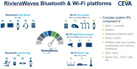
CEVA is already very well established in providing the communication part of this package. They are inside 9B+ devices shipped across multiple protocols, from BT/BLE and Wi-Fi up through all the cellular standards, and now offering 5G; specifically, Bluetooth and Wi-Fi solutions are provided through their RivieraWaves family. So it’s probably safe to assume they have communication part of the solution all wrapped up.
The standard choice for a CPU would of course be an ARM Cortex-M-class core – a safe bet and a big supporting ecosystem. But of course there’s a cost in licensing and royalties; this hasn’t historically been a big issue in premium devices but it could be a problem in price-competitive IoT devices. Which is one reason that RISC-V is attracting a lot of interest across the price-spectrum. Briefly on RISC-V, this is an open-source instruction-set architecture (ISA) developed originally in UC Berkeley and now available in open source implementations from Berkeley, ETH Zurich & University Bologna and in commercial implementations from Codasip, Cortus, Andes and SiFive (and others).
CEVA already provides the communications part of the software stack to run on an ARM platform, but given this growing interest in RISC-V, they now also offer turnkey hardware platforms including the “Zero-risky” open-source CPU implementation from the ETH Zurich & University Bologna, with FreeRTOS and communication stacks running on it (in this example for Wi-Fi). All you have to add is RF, sensor and peripheral interfaces, memory as needed, a real-time clock and your application software. All for a lower price than would be achievable with the standard platform which, Franz Dugand (Director of Sales and Marketing for Connectivity at CEVA) says is why one reason this platform is attracting a lot of attention.
According to Franz, the majority of customers they have today are using a more extended architecture in which this subsystem services all the communication functions, communicating through AXI with an application processor subsystem for more extensive processing. He tells me the Wi-Fi solution is scalable all the way from 802.11n up to ac/ax for big access points. What is different between these solutions is in implementation – clock frequency and memory size. Also the modems differ from one Wi-Fi version to another, from pure hardware implementations through software-defined, running on a DSP (naturally a core-strength for CEVA).
The turnkey solution for Bluetooth looks quite similar, with support for both low-energy and dual-mode operation and proven with both RivieraWaves and 3[SUP]rd[/SUP]-party RF.
CEVA provides FPGA-based evaluation boards hosting the Zero-riscy implementation of the RISC-V core along with, I believe, both Wi-Fi and BT/BLE options. They have run Wi-Fi benchmarking for their implementation against both Cortus and Cortex-M0-based solutions. Running each at the same clock frequency, they have been able to show comparable performance between across all three implementations.
One interesting point Franz made – he said they don’t ship ARM cores with their reference boards for the same cost reasons that customers may encounter. An obvious question for me was why they don’t use one of the SoC FPGAs which includes a built-in ARM core. His answer was revealing – they use low-end FPGAs (Spartan) to keep the board cost down. Using an SoC FPGA like Zynq would dramatically increase this cost. Also the SoC versions tend to use big processors (Cortex-A), where the CEVA target applications will more commonly be based on Cortex-M-class processors. Now with a Zero-riscy core, all those problems go away; the reference board and software are truly turnkey, and at a much more accommodating price-point.
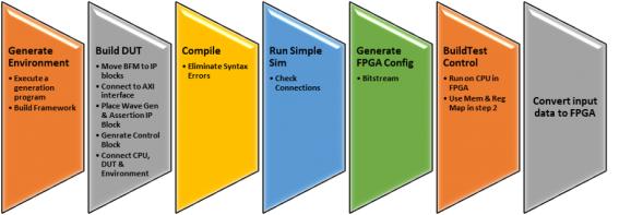
Franz wrapped up with a compelling datapoint on what it took for them to move from an ARM-based implementation to a RISC-V implementation:
- 1 week to build a new hardware platform (replace the CPU, run simulation, generate new FPGA binary)
- 1 week to port the software
- 1 week of system level validation
Three weeks is not a big investment to enable cutting your costs. You can learn more about CEVA RISC-V-based solutions HERE. There’s also an interesting viewpoint on how RISC-V is changing the game for IoT HERE.