I am very sorry but I have to break the flow of sharing initiatives, to reiterate the reason for these articles and maybe amplify the message these articles should promote.
I got a few inquiries from LinkedIn connections, who read the previous articles, with a very interesting point of view. This proves that after 5 articles some people did not get “yet” the message. They say that people like the stories, the explanations, the details, but I had a better chance to “invent” things as the world of VLSI automation was very “crude” and “primitive”. Today with all the automation going on, there is little to improve, improvise, innovate or invent. Most of what is needed is already here, so I should write about what should they invent next!!! If everybody will think this way we will stop growing, the gate size technology will stop “shrinking”, and the number of people in our industry will diminish.
To prove my point, I have to go back to history, my initial start in this profession. The year is 1984, the day is January 24, I was one of the 4 people selected to get trained in this “fancy” profession called IC Layout Designer. We were very excited recruits as the number of people with this profession was 6 in MSIL and in all Israel maybe 30 at that time. We were had a trainer from US to teach us Calma computer and software and for layout basics, flows and procedures our trainer was the Layout Manager, Miriam Zvuloni Gaziel. She had a challenging task: to get us from “know nothing” to people she can trust in 3 months. I can never forget the most shocking sentence she used at the end of the first training day:
As you will see, this is a very “fascinating” profession that you cannot learn anywhere else but in big companies like Intel, National, Motorola today. It will pay very well compare to other professions however, based on how the software automation is going, this profession has the potential to disappear in the next 5 years. This was in 1984.
I don’t want to invoke statistics but with all the automation the industry developed in in the last 30 years the number of IC Layout designers not only grew but exploded. Today there are many schools around the world teaching layout, Sankalp alone trained more than 1,000 new grads in the last 10 years. Universities are training Master and PhD student’s in layout so they can implement their projects in silicon. Only in India, that in 1983 probably had no VLSI development industry, there are more than 10,000 people doing VLSI today. We progressed from Calma mainframe to Linux machines, from 5 microns to 5 nano-meters. If somebody says that there is nothing else to invent because all is already there, they should move into the back seats and let the “inspired” and “creative” people take the driver and navigator seats. They will move forward, supporting new ideas, investing time and “Gray power” in new initiatives for automation and technology. Hopefully this clarification is understood and you can use my “historical stories” as stepping stones for your personal development without expecting others to tell you what to do.
A specific issue we had at MOSAID was that each project had to be developed in a totally new process so all tools setup had to be redone every time. We invented the Process Independent Setup (PIS) but people still needed to learn new design rules for each new project. In some cases, the rules changed while we were in the middle of the development. Luckily for us compaction engines showed up around 1996-1997. Rubicad from Germany and Sagantec originally from Holland, with later development moving to Israel. We did our homework by comparing the 2 company’s software features. I saw demos of both at DAC, some official some beyond that. I spoke with all the possible reference users they provided. The final decision was to invite Sagantec for an onsite demo.
We got a very strong AE to visit, Simon Klaver from Holland. The intention was that we can generate fast “dirty” cells and using compaction will get DRC clean results. We also wanted to see if we can use this technology to “migrate layout from process to process” a very new concept at that time. We gave Simon 2 cells for DREAM, the software name at that time, and ask him to clean all the design rules errors. We gave him 5 days with the hope that we can see some “good results” towards our target, but in 2 days he provided DRC and LVS clean cells. Case closed, we needed this tool, so we bought it. MOSAID bought the first DREAM license in North America at a good price with good maintenance service agreement.
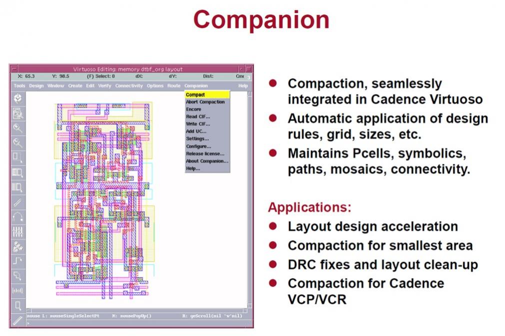
After all, this was a huge risk for such a small company to buy a new “bleeding edge” technology from an unknown EDA vendor. We worked directly with the development team and their AEs so Malcolm MacIntosh, one of my team members became our expert. For the next 3 years I spoke with all new potential customers, being the reference customer for Sagantec. This helped their sales and me making new friends around the globe… The following 5 years I was close to Sagantec and help them develop the roadmap for new tools, at the same time being one of the first users for some. One year, after DAC, I went for dinner at the house of Hein van der Wildt, the CEO at that time. After dinner I started to talk with him and Coby Zelnik, a developer at that time, about what can we do next with DREAM. I wanted a tool that can run inside my layout editor, and we started to explore what is needed to make this happen. Like in all cool stories we actually wrote ideas on the napkins we used from the dinner, full of pasta sauce and red wine…
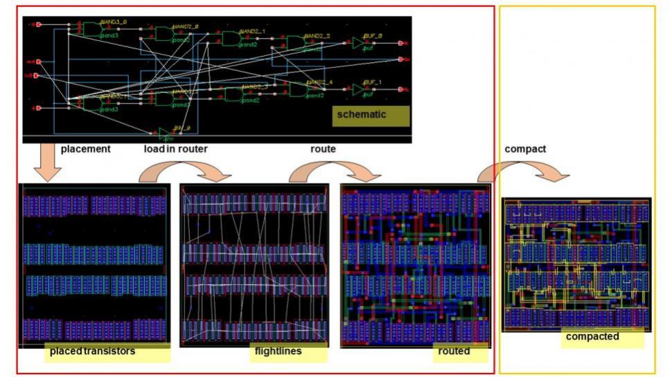
That night Companion, the idea of compaction inside Virtuoso was born.
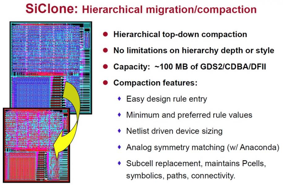
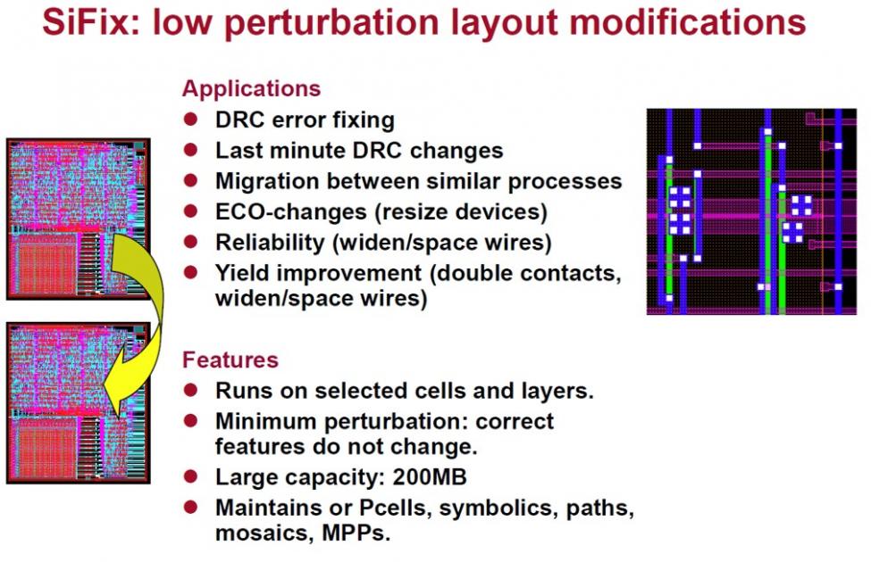
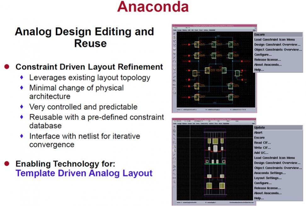
From compaction flat we wanted hierarchical, from compaction we planned migration, so the life was exiting every time I met their team. I had, and still have, many “interesting” conversations on the roadmaps with Maarten Berkens, who was their CTO at that time, and now is in Sage software. SiClone, SiFix, Anaconda each had a lot of fun to be part of their initiation and development. Being so involved in Sagantec payed back many years later. While in PMC Sierra we needed a tool for DRC fixing so we looked at VLM from Cadence and SiFix from Sagantec. Coby Zelnik, now the CEO of Sagantec, came to Vancouver with Christen Decoin to show the tool and talk about the corporation new capabilities.
Unfortunately, he had to leave in the middle of the night having a family situation. Christen was a new AE with good technical knowledge of the tools but did not know how to answer all customers questions. He did the demo and I became the presenter of Sagantec corporate and technical presentation to PMC Mixed Signal Design & Layout. I had fun convincing PMC team that the tool I present (as Sagantec marketing) is the tool I want (as PMC Sierra Layout Manager) and it’s doing what we needed. The crowd had a lot of fun punishing me with questions, but I survived and we bought the tool.
More MOSAID “non-layout” initiatives next month…
Dan
Read the full blog series HERE.
Share this post via:


Is Intel About to Take Flight?