You are currently viewing SemiWiki as a guest which gives you limited access to the site. To view blog comments and experience other SemiWiki features you must be a registered member. Registration is fast, simple, and absolutely free so please,
join our community today!
I am very sorry but I have to break the flow of sharing initiatives, to reiterate the reason for these articles and maybe amplify the message these articles should promote.
I got a few inquiries from LinkedIn connections, who read the previous articles, with a very interesting point of view. This proves that after 5 articles some … Read More
Major semiconductor company successfully migrated 28nm libraries to 14nm FinFET
Santa Clara, California – May 29, 2013 – Sagantec announced that its nmigrate tool was adopted by a major semiconductor company for the development of standard cell libraries at 14nm and 16nm FinFET technologies.
This customer already… Read More
It is important to note that the System On Chip (SoC) revolution that is currently driving mobile electronics has one very important enabling technology and that is Semiconductor Intellectual Property. Where would we be without the $6B+ commercial semiconductor IP market segment? Computers and phones would still be on our desks… Read More
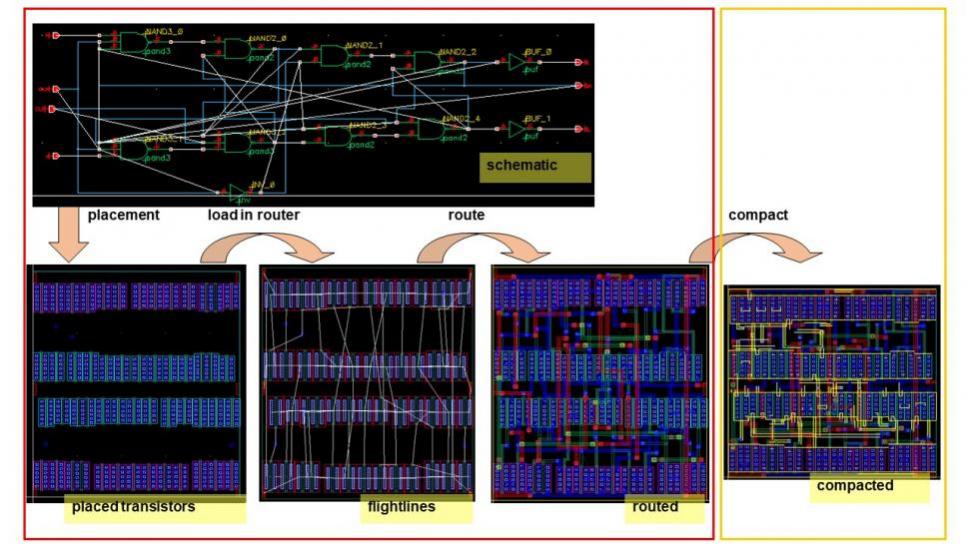
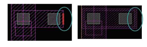
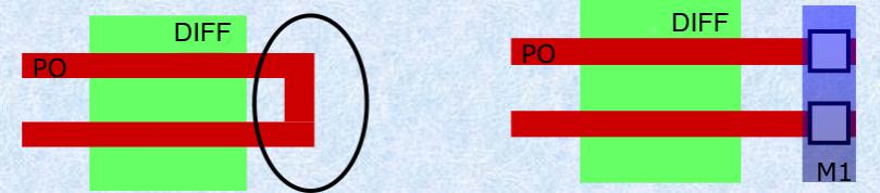
In the world of sub-40nm IC design, as feature size decreases with each new process node, it becomes increasingly difficult to migrate a layout to a new process technology. Too many factors impact manufacturability and yield. At each new process node, to make sure that a given layout is manufacturable and yields well, it is subject… Read More
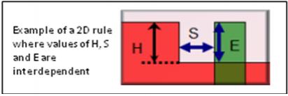
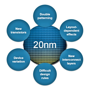
Adding sophisticated 2D dynamic compaction technology to address 20nm and 14nm challenges. Santa Clara, California – May 3 ,2012 – Sagantec today announced that it has acquired Dutch startup NP-Komplete Technologies BV (Eindhoven, The Netherlands) for its physical design compaction and migration solutions based on a sophisticated… Read More
Sagantec is the leading EDA provider of process migration solutions for custom IC design. Sagantec’s EDA solutions enable IC designers to leverage their investment in existing physical design IP and accomplish dramatic time and effort savings in the implementation of custom, analog, mixed-signal and memory circuits… Read More
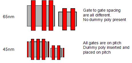
The problem:To move a single lane variable data rate SerDes (serializer-deserializer) from a 65nm process to a 45nm process, achieving a maximum performance of up to 10.3 Gbps. This is a large piece of complex mixed-signal IP with handcrafted analog circuits. Circuit performance and robustness are critical and must be maintained… Read More
A High-Definition Multimedia Interface (HDMI) IP core was being implemented in an advanced process technology. This fairly large and complex analog mixed-signal (AMS) IP comprising over 130K devices was close to being finalized and shipped to the customer. But many design rules at the foundry were unexpectedly changed from… Read More
The problem:To move dual-port SRAM library and macros from a 40nm process to a 28nm process. In addition to all the changes between two different foundry processes, the 28nm rules are disruptive and incompatible with the previous rules. The memory corecells (foundry-specific) would also need to be completely replaced.
Current… Read More
In the name of blogging and increased transparency lets talk about wafer allocation, because it’s coming, believe it. There is already a significant delta between wafer demand and manufacture due to record low inventory levels and the exploding semiconductor demand in China. Both TSMC and UMC posted good July sales numbers: … Read More