Talking to customers is one of the best parts of being a semiconductor professional. It keeps you grounded and offers you the collective experience of some of the smartest people around the world, absolutely.
Webinar: The Emergence of FPGA Prototyping for ASIC/SoC Design
Customer success stories are a close second and interestingly much harder to come by than a face to face meeting. The semiconductor industry is very competitive (secretive) so when you do get a customer willing to speak up it is definitely worth your time. This success story is from my favorite FPGA Prototyping provider S2C:
Inspur is a leading cloud provider in China offering high-end servers, mass storage, cloud operating system, and information security technology. As a chip and systems developer Inspur was faced with the challenges of establishing an executable platform for hardware validation and integration, building a high bandwidth transmission channel to transfer mass packet to DUT for verification, and supporting fast and stable system startup then quickly and accurately locating problems.
Inspur’s routing control design consumed 96% BRAM of VU440 FPGA which allowed no extra memory resources for ChipScope debugging. The S2C delivered MDM does not consume design FPGA memories which perfectly solved this debugging issue.
The complexity of Inspur’s SoC increased both cost and schedule risks due to the need to verify real-world scenarios. Generally no one knows when a bug will hit or when it actually occurs, especially if there isn’t enough sampling depth to analyze. MDM mitigated those challenges as a cost-effective solution. After the initial 1~2 MDM and Single VU systems bring up, Inspur used 10 sets of systems running 24 hours a day without interruption. This enabled Inspur to detect and fix many bugs in the real network testing environment which cut six months off their development schedule.
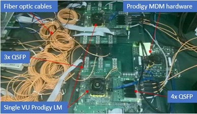
Inspur used the Single VU440 Prodigy Logic Module for prototyping verification on a routing control chip and selected the MDM to run the deep trace debugging which allows Inspur to grab as many packets as possible to then be analyzed for correctness.
“The performance capabilities of the Prodigy Logic Module, deep trace debugging of MDM software, professional daughter card customization services, and fast support helped us efficiently verify our SoC designs. This allowed us to focus on the innovation and validation of the SoC.” Said Huang Jiaming, General Manager of High-end Server Department at Inspur.
“The biggest advantage S2C MDM gives us is the ability to detect bugs deeply embedded in the design that can be detected only by processing the real word packets. This significantly speeds up the debug process and gets our design to the market quickly with greater confidence.”
Overview
- S2C’s single VU440 Prodigy Logic Module providing multi-million ASIC gate capacity
- The Prodigy Multi-Debug Module (MDM) enables greater sampling depth which makes debugging easier
- The customized QSFP Interface Module is well designed and higher performance
- The quick response of S2C’s support team helped Inspur to bring up the FPGA validation environment successfully
With S2C’s rapid SoC prototyping solutions Inspur saved about six months in developing and debugging their SoC design. Features like scalability, reuse, flexibility, and deep trace debugging let Inspur quickly port the design into FPGA prototyping, transfer mass packet to the DUT, and speed up the debugging progress.
S2C Solution
- S2C’s Single VU440 Prodigy Logic Module providing multi-million ASIC gate capacity allows Inspur to quickly port their routing control chip for verification
- Customized two QSFP cage interface modules to provide the high-speed transmission channel for the DUT
- Specialized Prodigy Multi-Debug Module hardware enables deep trace debugging with the ability to store up to 16GB of waveforms
- Prodigy Player Pro is used to setup trigger conditions and capture related packets for chip-level debugging

Figure 1: Inspur routing controller validation platform using S2C Single VU440 + MDM
About S2C
Founded and headquartered in San Jose, California, S2C has been successfully delivering rapid SoC prototyping solutions since 2003. S2C provides:
- Rapid FPGA-based prototyping hardware and automation software
- Prototype Ready™ IP, interfaces and platforms
- System-level design verification and acceleration tools
With over 200 customers and more than 800 systems installed, S2C’s focus is on SoC/ASIC development to reduce the SoC design cycle. Our highly qualified engineering team and customer-centric sales force understand our users’ SoC development needs. S2C systems have been deployed by leaders in consumer electronics, communications, computing, image processing, data storage, research, defense, education, automotive, medical, design services, and silicon IP. S2C is headquartered in San Jose, CA with offices and distributors around the globe including the UK, Israel, China, Taiwan, Korea, and Japan. For more information, visit www.s2cinc.com.
Share this post via:


Comments
There are no comments yet.
You must register or log in to view/post comments.