When starting SemiWiki we focused on three market segments: EDA, IP, and the Foundries. Founding SemiWiki bloggers Daniel Payne and Paul McLellan were popular EDA bloggers with their own sites and I blogged about the foundries so we were able to combine our blogs and hit the ground running. For IP I recruited Dr. Eric Esteve who had never blogged before but he took to it quite quickly. I knew Eric from his IP reports at my previous position working with the foundries at Virage Logic.
Since going online in 2011 SemiWiki has published 693 IP related blogs with 3,572,124 views. Eric has written 277 of those blogs averaging close to 6,000 views per blog. Today Eric is by far the most respected IP analyst with the most detailed and accurate reports and it is an honor to work with him, absolutely.
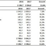
According to the Design IP Report from IP-Nest the market is still doing very well with YoY growth of 12.4% in 2017. The ARM Group of Softbank (previously known as ARM Holdings) is again a strong #1 with IP revenues (licenses plus royalties) of $1,660 million and 46.2% market share, followed by Synopsys growing by 18% to $525 million and 14.7% share. Broadcom, being the addition of Avago + LSI Logic + Broadcom, is making an entry in the top 3, replacing Imagination. Both Cadence and CEVA are showing 20%+ growth in 2017.
IPnest has defined 11 categories ranking IP vendors. The CPU IP category is the largest with about 42% of revenues from design IP. There are strong disparities between CPU, DSP, and GPU & ISP as the weight of the CPU category is about 9x the DSP and 5x the GPU/ISP.
ARM is obviously #1 in the CPU category, and will probably keep this position for a long time due to the royalty mechanism. Nevertheless, we can see that ARM CPU IP license revenue has declined by 6.8% YoY, more than compensated by the royalty revenue growing by 17.8%. The reasons may be multiple. After the ARM acquisition by SoftBank, the accounting policy was changed creating what Eric calls an “artifact”. However, in my opinion we are starting to see the impact of RISC-V becoming a credible alternative to the ARM CPU hegemony. The 2019 Design IP report should confirm this.
In the Processor group (CPU + DSP + GPU & ISP), Imagination Technologies (IMG) is still #2 but I expect their royalty revenue to collapse when Apple effectively moves to an internal GPU solution. Now, if we consider the followers, both CEVA and Cadence have made 20%+ progression in 2017, then it wouldn’t be surprising to see one of these two companies becoming the #2 next year. In my opinion it will be CEVA but in any case the ranking in the Processor group will be disrupted next year.
The next group after Processor is the Physical IP, including: Wired Interface IP, SRAM memory compiler, other Memory Compilers, Physical Libraries, Analog and Mixed-Signal and Wireless Interface IP.
If we look at the Wired Interface IP category, it’s now at $735 million (20% YoY growth) and 20.5% of the total. Synopsys is the clear leader with about 45% market share, as well as in the Physical IP group with 35% market share.
If you take a look at the picture above you can see an interesting trend; the 2016/2017 evolution of the Wired Interface IP as a portion of the total moves from 19% to 20.5% when Processor IP declines from 58.3% to 56.4%.
As forecasted by IPnest in the “Interface IP Survey & Forecast”, the Wired Interface IP should reach $1 billion in a few years (2021 or 2022). Even though ARM is giving up in China through a so-called “joint venture”, the Wired Interface IP category will remain an island of (growing) stability in the 2020s.
Increasing complexity: can you imagine that the DDR5 memory controller PHY is now running at 4400 Mb/s? This is also 4.4 Gb/s or almost the PCIe Gen-2 data rate (5 Gb/s), which was one of the IP stars 10 years ago.
Eric was chairman of a panel during DAC 2017 “Growing IP market despite semi consolidation” and this panel came to a consensus: The IP market in 2010-2020 is like the EDA market in 1980-1990, outsourcing was the rule and the result was an EDA market completely externalized by 2000. As long as a function is not perceived as a differentiator by a design team, it can be outsourced and it will become an IP sold by commercial vendors (see the Top 10 list).
Bottom line: If you apply a 12% CAGR for the next 5 years you can easily predict a $6 billion IP market in 2022.
To buy this report, or talk to Eric you can contact him at eric.esteve@ip-nest.com. He will also be at DAC again this year if you want to meet him.