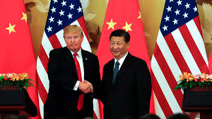
Bronco Webinar 800x100 1

Machine Learning Neural Nets and the On-Chip Network

Machine Learning Neural Nets and the On-Chip Network
by Bernard Murphy on 03-15-2018 at 7:00 am

Machine learning (ML), and neural nets (NNs) as a subset of ML, are blossoming in all sorts of applications, not just in the cloud but now even more at the edge. We can now find them in our phones, in our cars, even in IoT applications. We have all seen applications for intelligent vision (e.g. pedestrian detection) and voice recognition (e.g. speaker ID for smart speakers). In a compelling demonstration of just how widely application is spreading, one IP vendor recently announced a 5G modem sub-system using neural nets in support of link-adaptation (optimizing the link between the UE and the base station). The sky truly seems to be the limit for this technology.


An important question for this audience is what hardware architectures are needed in support of these systems, particularly at the edge. Here power/energy is much more important than in the cloud, yet performance is also important to complete complex recognition tasks in milli- or micro-seconds (long/variable delays are sub-optimal when deciding if the car needs to slam on the brakes).

Also, while we originally thought that we only needed to do training in the cloud and could do skinnied-down inference at the edge, now we’re finding applications where re-training at the edge becomes important. Your car has driver face-ID, you break your leg on a hike in the remote backwoods, fortunately someone is with you so can drive you to the hospital, but they never trained the car to recognize them and, oops, there’s no cell reception to support cloud-based training. In this case, maximally-reduced NNs (which can’t support local training) may not be the way to go.

All of which means that often there is no one best architecture choice; platforms must host a range of options to suit different needs. The range can be pretty wide – GPUs with fixed-point compute (lower power than floating-point), also specialized accelerators: FFTs, custom vector and matrix compute engines, support for flexible operand bit widths (8->4->2) through NN flows, and low word-size weights. More specialized still are architectures such as grids of interconnected processing elements, offering higher performance at lower power through closely-coupled compute for NN (and I would guess neuromorphic) applications.

A common factor in all these applications is minimizing DRAM accesses, since each neuron MAC operation requires 3 reads (weight, activation and partial sum) and one write (new partial sum). In AlexNet, a well-known reference network in the domain, 3 billion memory accesses are required to complete a recognition. If all this went straight to DRAM, performance and power would be wildly impractical. In conventional compute architectures you mitigate with layers of caching. In some of these more exotic architectures, multiple caching strategies are required – local register files, closely-coupled memories, internal (to the accelerator) SRAM and common buffer RAMs.

Cache coherence then becomes important at the accelerator level and at the SoC level. NN algorithms are very regular but intrinsically 2-D (for image recognition at least) and area-performance tradeoffs limit how much tightly-coupled memories can hold. As you might guess, given this problem definition, there are multiple strategies for optimizing locality of reference – around weights, around MAC outputs, even around rows in the (current) image. Whichever strategy is employed, in large systems and systems supporting feedback such as RNNs, processing elements ultimately have to share memory (also with the CPU/ GPU subsystem running the show), which of course they must do coherently if recognition is not to become scrambled.


I wrote in my last blog about how Arteris supports cache-coherent connectivity through their Ncore 3 interconnect fabric and how non-coherent peers on a FlexNoC interconnect can tie into the coherent network through proxy caches. This has apparently become of particular interest in integrating NN accelerators which can use these proxy caches to sync not only with the main coherent network but also with each other. An added benefit is that these caches can be optimized to use-case needs which is important for such specialized architectures.

Ncore also provides support for functional safety in the generated interconnect, a must-have for ADAS and autonomy applications these days. They do this through a Resilience option to Ncore, providing data protection (parity for data paths and ECC for memory paths), intelligent unit duplication and checking (similar to dual-core lockstep – DCLS), and a fault controller with BIST that is automatically configured and connected based on the designer’s data protection and hardware duplication settings. These capabilities can be combined to provide sufficient diagnostic coverage to meet automotive ISO 26262 functional safety certification requirements, as well as the more general IEC 61508 specification.


Arteris are obviously making waves, judging by the list of companies that have adopted their solutions for ML/NN applications. I would guess that differing adoption of Ncore versus FlexNoc reflects the wide range of architecture approaches I discussed earlier. You can learn more about the Arteris solution and AI HERE. If you have the patience for a long paper, THIS is an excellent read on differing approaches to hardware for NNs.


New Architectures for Automotive Intelligence

New Architectures for Automotive Intelligence
by Tom Simon on 03-14-2018 at 12:00 pm

My first car was a used 1971 Volvo 142 and probably did not contain more than a handful of transistors. I used to joke that it could easily survive the EMP from a nuclear explosion. Now, of course, cars contain dozens or more processors, DSP’s and other chips containing millions of transistors. It’s widely expected that the number of CPU’s alone could run into the hundreds as new infotainment and autonomous driving features are added.

Automotive intelligence electronics are rapidly evolving, but relatively speaking are in their infancy. The best arguments for this assertion are the huge changes forecast for powertrain, Infotainment, automation, safety and connectivity in cars for the foreseeable future. With rapid change and its relative youth, we can expect dramatic evolution of the internal architecture of automotive electronics. This evolution will recapitulate the evolution of computing and the internet. After all cars are a microcosm of the larger computing landscape.

We see each player in the market looking to shape the prevailing architecture around their own product strengths. Qualcomm, Nvidia, NXP, Cadence and Synopsys and many others, each have their own computing paradigm. Nvidia of course if pushing for centralized GPU based processing, Qualcomm is looking to leverage 5G and communication. Vision processing IP providers are proselytizing for their products.

The growth of the internet led to the expansion of distributed computing, and consequently computation work moved from mainframes to local nodes. Eventually IoT combined the models with edge sensor fusion and central processing. It’s likely that in cars sensor fusion will take place closer to the sensors, and central processing will be used for tasks that require integrated data from multiple automotive systems.

I had a chance recently to read a white paper by Achronix that explores the choices and coming evolution of onboard computing. Achronix posits that immense amounts of data will be generated by onboard sensors, which in turn will place heavy demands on data links processing units and strain power distribution and dissipation abilities. Also, they mention that reliability as enabled by real-time testing and diagnostics will become even more important. Achronix offers a unique option to ameliorate reliability, power, data and processing issues. Their embedded FPGA fabric, known as Speedcore eFPGA can work in multiple ways to improve and futureproof automotive systems.

As systems move toward sensor fusion at the edge, having SOC’s with processors and programmable eFPGA fabric will improve throughput and allow for flexibility as the needs for processing algorithms change. CPU’s will not have to intermediate all data transfers because eFPGA fabric can perform DMA without requiring CPU IRQ’s. The ability to perform lookaside processing will be a major factor in system performance.

SOC’s with embedded FPGA fabric can help manage the onboard data networks – including Ethernet, as well as legacy and future automotive networks. These SOC’s will be optimized for packet handling and data filtering on the fly.

Finally, higher level processing can also benefit by hardware acceleration through eFPGA. FPGA’s are already being used for this in data centers, but eFPGA avoid costly SerDes transfers, higher part counts, and overprovisioned general purpose commercial parts.

However, eFPGA comes into its own when we talk about reliability. Each eFPGA core can become a real-time embedded hardware diagnostic engine if needed. With full bus access and reprogrammability, eFPGA can be used to generate tests to ascertain the operating condition of chips and system in running vehicles or during servicing.

The Achronix white paper, entitled Speedcore eFPGA in Automotive Intelligence Applications does a good job of introducing the issues faced by automotive system designers. It also covers several approaches to Automotive Intelligence and closes by outlining the ways that eFPGA can improve overall system performance.


CEO Interview: Ramy Iskander of Intento Design

CEO Interview: Ramy Iskander of Intento Design
by Daniel Nenni on 03-14-2018 at 7:00 am

One of the more interesting parts of blogging for SemiWiki is getting to know emerging EDA and IP companies from around the world. As I have mentioned before, there are some incredibly intelligent people in the fabless semiconductor ecosystem solving very complex problems. It is a two way exchange of course since we know the market for their products intimately through our work on SemiWiki and experience as working semiconductor professionals. I first met Ramy at #54DAC in Austin which brings us to this interview:

Please tell us about Intento Design?

Intento Design is a French company located in Paris. The company started with a strong understanding of EDA and a desire to improve analog design automation. Currently, analog design has less automation than digital design and, because of this, it remains the bottleneck of integrated circuit system development. And I say system development because that’s where the value is in the today’s semiconductor market. As we move up the value chain toward increasingly complex integrated systems, the ability of a semiconductor company to capture value in a timely manner is put at risk by analog design schedule delay. Conversely, the relative contribution to system level value is large from the analog circuitry as these disproportionately impact real world performance factors – such as signal-to-noise quality and power consumption.

What makes Intento Design unique?

First, let’s talk about what makes analog designers unique, then I can explain Intento Design to you. Often you hear that analog design is an art more than a science, and there’s a lot of truth to that statement. Innovation in analog design takes place at the schematic where local feedback loops can be visualized. Take the schematic away and the analog design creativity vanishes. This is what makes Intento Design unique – our products are schematic centric, allowing the analog designer to benefit from advanced automation, be able to move between process technologies and yet still retain the schematic view.

At Intento Design we know the combination of a circuit schematic together with the designer intentions, which is just another way of saying engineering “know how” by the way, is far more than the sum of the parts. In fact, these two information structures, the schematic view and the designer intentions, carry substantial information only when they are put together. Clearly, someone untrained in the art, so to speak, could fail to appreciate an analog circuit schematic without an explanation!

Intento Design is the first company to formalize a process of attaching an intention view to the schematic. Interestingly, we’ve managed to do this in a technology independent manner which gives analog designers unlimited exploration capacity to move their schematic design into different technology processes seamlessly.

What keeps analog designers up at night?

The analog designers that I know love what they do, and often what is keeping them up at night is thinking about circuit design! It’s an incredibly creative profession. To design and innovate, designers must achieve a deep understanding of both their schematic circuit and the process technology. The main problem that causes analog designers, and their managers, to lose sleep is that there is simply not enough time in the schedule to achieve new levels of performance or to innovate for novel analog function.

To get to system integration and verification faster, the analog design phase must be accelerated. However, in today’s complicated process technologies, the analog design phase is now actually taking longer than before, and designers still need more time. The novel ability to create a design intention view and complete an exploration of the intended performance trade-offs using Intento Design tools in any technology gives analog designers a substantial time advantage.

How can ID-XPLORE help?

The core technical capability of ID-XPLORE is highly automated exploration of the performance limits of any schematic circuit in any process technology. By providing the ability to quickly and accurately explore schematic changes in a technology, ID-XPLORE helps designers to innovate analog circuits, migrate between technologies and to meet challenging design specifications on schedule.

For example, to resize a schematic in a different technology with the same, or new, performance specifications, something which can currently take a design team a few weeks to complete, can be done in a single day with the help of **ID-XPLORE. For design acceleration, very challenging circuit design problems which can take a skilled analog designer over week to understand and resolve can be re-designed in just hours using data coming from the ID-XPLORE tool. This level of disruptive innovation is possible because the ID-XPLORE works at the schematic level but provides novel, exhaustive and very data-intensive exploration results quickly.

At Intento Design, we made it our goal to create a tool that enables analog designers to reach the speed of digital circuit design very seamlessly. ID-XPLORE is a plugin tool which works in existing schematic centric design flows. This allows analog designers to stay focused on schematic innovation, while ID-XPLORE provides rapid transistor sizing and design insight.

Can you provide some real world examples?

Yes, absolutely. In addition to design acceleration and technology migration, or technology porting as it is sometimes called, we are starting to see some very specific and interesting use cases which I can tell you about.

A recent case was a performance issue in a OTA where the open-loop gain was compromised (too low) during one phase of a switched-capacitor common-mode feedback. The analog designers had worked for a couple of weeks without a definitive architectural solution, but they were reluctant to increase power consumption. Because ID-XPLORE operations are SPICE accurate, a definitive answer can actually be obtained, and fast. The analog designer constrained the DC bias range and ID-XPLORE was used to calculate the transistor sizing and testbench performance evaluation for various DC bias points within the constrained range. Within hours, the ID-Xplore tool completed exploration over a range of millions of points and returned solutions that allowed the designer to fully understand their design trade-offs.

Being able to obtain a definitive “yes” or “no” answer for schematic circuit performance in a technology has been of high interest to recent clients. This capability is a results of the automated, high-speed operations of ID-XPLORE which provides rapid transistor re-sizing and performance analysis. The operations can extract a hard limit or a trend within a technology helping the designer to make decisions. The designer can pursue an alternative schematic topology or present the accurate performance trade-offs obtained by ID-XPLORE to the system team for decisions on issues such as power and performance.

Yet another case is where ID-XPLORE was used in the design of a multi-stage, 100-transistor amplifier inside a power-control circuit. In this case, there was a need to push speed performance significantly past existing best-in-house design by 30%. Using ID-XPLORE, the designer achieved the target performance increase is less than a day. But, in addition to this, ID-XPLORE identified a design solution that allowed much smaller transistors at the output stage compared with existing in-house design efforts. Reduction of the output stage transistor sizing allowed a significantly reduced layout area.

Because of the exhaustive exploration capability, which is simply not possible with other tools, this client and others consider the ID-Xplore tool as a kind of “reasonability check” for their own carefully crafted design solutions. When analog designers make decisions for performance versus power trade-offs, their design results can sometimes end up going down a path which leads to unnecessarily oversized transistors.

Which markets do you feel offer the best opportunities for ID-XPLORE over the next few years and why?

The semiconductor industry is constantly changing and ID-Xplore is relevant in many emerging industry contexts. ID-Xplore is currently seeing a large opportunity in technology migration for IP-Portfolio partnerships, as well as corporate mergers where product lines must align newly acquired IP over several technologies.

For the analog designer, the raison d’être of ID-XPLORE, the tool is particularly useful in situations where the performance of the circuit pushes the limits of the technology. Growth in mobile embedded systems, such as IoT, presents a large opportunity for ID-XPLORE as these circuits require extremely low-power operation which is often achieved with innovative circuitry in localized bias conditions. As we head toward more and more applications using mobile embedded systems, power and area efficiency are increasingly competitive positions for semiconductor companies to hold and ID-XPLORE can help them achieve this.

http://www.intento-design.com/

Also Read:

CEO Interview: Rene Donkers of Fractal Technologies

CTO Interview: Ty Garibay of ArterisIP

CEO Interview: Michel Villemain of Presto Engineering, Inc.


Webinar Alert – Embedded Monitoring of Process and Voltage in SoCs

Webinar Alert – Embedded Monitoring of Process and Voltage in SoCs
by Daniel Payne on 03-13-2018 at 12:00 pm

In the old days to learn about new semiconductor IP you would have to schedule a sales call, listen to the pitch, then decide if the IP was promising or not. Today we have webinars which offer a lot less drama than a sales call, plus you get to ask your questions by typing away at the comfort of your desk, hopefully wearing headphones as to not disrupt your co-workers at the next cubicle. I’ll be attending a webinar from Moortec about their IP for monitoring process and voltage variations on April 25, 10AM PDT and invite you to join the event online. After the webinar I’ll write up a summary of the salient points, saving you some time and effort in the process if you cannot attend virtually.

Intro
Historically temperature has always been the first thing engineers think about when it comes to monitoring in-chip conditions, however as we move into more complex designs on advanced nodes, process and voltage start to become equally critical considerations. The associated challenges manifest in multiple ways, including: process variability; exposure to timing violations; excessive power consumption; and the effects of aging. Each of these can lead to ICs failing to perform as expected.

Webinar Content
In this latest Moortec webinar we will look at how process and voltage monitoring combine to enhance the performance and reliability of the design and how they can be used to implement various power management control systems.

This webinar is aimed at IC developers and engineers working on advanced node CMOS technologies including 40nm, 28nm, 16nm, 12nm and 7nm. It will seek to outline the two main pressures that designers are grappling with today, being: i) the desire for lower supplies, enabling compelling power performance for products, especially consumer technologies; and ii) the challenge posed of placing in jeopardy the functional operation of SoCs and an entire product range. The dilemma for the designer is that to maximize the former, optimization schemes used today are algorithmically treading an increasingly thinner line between robust operation and having failing devices within the field

Moortec provide complete PVT Monitoring Subsystem IP solutions on 40nm, 28nm, FinFET and 7nm. As advanced technology design is posing new challenges to the IC design community, Moortec are able to help our customers understand more about the dynamic and static conditions on chip in order to optimize device performance and increase reliability. Being the only PVT dedicated IP vendor, Moortec is now considered a centre-point for such expertise.

After registering, you will receive a confirmation email containing information about joining the webinar.

Webinar Registration
It’s easy to register online here for Wednesday, April 25 at 10AM PDT (US, Europe, Israel).

About Moortec Semiconductor

Established in 2005 Moortec provides compelling embedded sub-system IP solutions for Process, Voltage & Temperature (PVT) monitoring, targeting advanced node CMOS technologies from 40nm down to 7nm. Moortec’s in-chip sensing solutions support the semiconductor design community’s demands for increased device reliability and enhanced performance optimization, enabling schemes such as DVFS, AVS and power management control systems. Moortec also provides excellent support for IP application, integration and device test during production.

Related Blogs


Another Application of Automated RTL Editing

Another Application of Automated RTL Editing
by Bernard Murphy on 03-13-2018 at 7:00 am

DeFacto and their STAR technology are already quite well known among those who want to procedurally apply edits to system-level RTL. I’m not talking here about the kind of edits you would make with your standard edit tools. Rather these are the more convoluted sort of changes you might attempt with Perl (or perhaps Python these days). You know, changes that need to span multiple levels of hierarchy, looking for certain types of block, then adding, removing or changing connections which also cross hierarchy. Technically possible with custom scripts perhaps but these can get really hairy, leaving you at time wondering if you’re battling on out of a stubborn refusal to quit or because that’s really the best way.


DeFacto originally got into this space in support of DFT teams who need to add and connect complex BIST logic which may have to be reconfigured on new RTL drops and reconfigured again on floorplan changes. Their big value-add is in making these edits easily scriptable without demanding that you tie yourself in knots figuring out hierarchy implications. Since they can edit RTL, and such needs are common beyond DFT, their customers have expanded use of these tools into many other applications, each of which needs at least a subset of those complex find, restructure, edit, re-stitch and similar operations.

One such use-model was announced recently – using scripted editing to trim down SoC RTL in order to greatly accelerate simulations. The design application in the case was in graphics, a domain which has lots of repeated block instances, in common with quite a lot of other applications like networking. Also in common with those applications, these designs tend to be huge. Now imagine you have to simulate this monster – yes, simulate, not emulate or prototype. Why on earth would you do that? Lots of reasons – you have to include AMS in your verification, you have to do 4-state modeling (0, 1, X, Z), you need to do on-the-fly debug, it’s faster to experiment in simulation, or maybe acceleration hardware is tied up on another project. But compile and simulation on the full core/chip will take forever.

Fortunately, a lot of verification objectives don’t require the simulator to swallow the whole design. You can trim repeated instances down to just one or a few instances, replacing the rest with shell models. But this isn’t quite as simple as black-boxing. First and most obviously a black-box outputs will float at X, which will mess up downstream logic. So at minimum you have to tie these outputs off, inside the black-box.

But even that isn’t quite enough. Integration logic often depends on handshake acknowledgement. If I send you a req, you better respond with an ack at some point, otherwise everything locks up. So now you have to add a little logic (again inside the black-box) to fake that req-ack handling. And so on. The shell starts to accrete some logic structure just to make sure it behaves itself while you focus on the real simulation. This may extend to keeping whole chunks of a logic block while removing/tying off the rest. So much for simple black-boxing.

This is a perfect application for the DeFacto toolset, as Synapse Design observed in their endorsement of STAR. They found that some simulations they were running would take 3 weeks – each. But many of the sims only exercised subsets of the system, in some cases only needing certain instances in a repeated set, in others requiring only a part of the functionality of a module. By intelligently exploiting scripted edits over the design, they found they were able to reduce these simulation run-times by 4X (in one case by 5X). That’s a pretty huge advantage in getting to verification closure.

I’m a strong believer in this kind of scripted RTL editing/manipulation. There are many tasks through design and verification (and touching even implementation) which beg for automation but don’t easily fall into canned solutions. Many design teams hack scripts or simply accept they can’t do better when they hit these cases. There is a better way which doesn’t constrain your ingenuity and control but does automate the mechanical (and very painful) part of the job. Check it out.

Also Read

Analysis and Signoff for Restructuring

Design Deconstruction

Webinar: How RTL Design Restructuring Helps Meet PPA


Clock Domain Crossing in FPGA

Clock Domain Crossing in FPGA
by Alex Tan on 03-12-2018 at 12:00 pm

Clock Domain Crossing (CDC) is a common occurrence in a multiple clock design. In the FPGA space, the number of interacting asynchronous clock domains has increased dramatically. It is normal to have not hundreds, but over a thousand clock domains interactions. Let’s assess why CDC is a lingering issue, what its impact and the available remedy guidelines to ensure a robust FPGA design.


CDC occurs whenever data is transferred from a flip-flop driven by one clock to a flip-flop driven by another clock. CDC issues could cause significant amount of failures in both ASIC and FPGA devices. The consequence of CDC is a metastability effect which leads to either functional non-determinism (unpredictability of downstream data, which could also yield to data loss) or data incoherency (when CDC induced delayed latency on subset of bus signals being sent across, causing non-uniform capture event).

Metastability and Synchronizer — As illustrated in Figure 1, metastability may be present in design utilizing flip-flop. Any flip-flop could be made into such state by concurrent toggling of input data and sampling clock (in the diagram the concurrent switching window of the underlying gates introduced leakage current). The known approach to neutralize the effect of metastability is by the use of synchronizer. A synchronizer can be defined as a logical entity that samples an asynchronous signal and outputs a derivative signal synchronized to a local sampling clock. It is usually not synthesized, instead pre-instantiated in the design or presented as a macro. A good synchronizer should be reliable, have low latency, power and area impact. The simplest implementation is using two back-to-back flip-flops. The first flip-flop samples the asynchronous input signal into the new clock domain and waits for a full clock cycle to permit any metastability to settle down. The output signal of the first stage is sampled by the same clock into a second stage flip-flop to produce a stable and synchronized output.

Data Synchronizers — Two basic methods are available for transferring data signals across clock domain boundaries. The first is based on enable-controlled data capture in the receiving domain, while the second is based on sequential writing and reading of data using a dual-port FIFO.

Control-Based Data Synchronizers – in this type of synchronizers, the enable signal is responsible to inform the receiving domain that data is stable and ready to be captured. The transmitter is responsible for keeping data stable over time while data enable is asserted. The stability of all data bits during received data capture guarantees an absence of the metastability effect and correct data capture. Figure 2 shows variation of control based data synchronizers:
– Mux-based data synchronizer
– Enable-based data synchronizer
– Handshake-based data synchronizer

To achieve safe data capture, the control-based data synchronizer should make sender data stable, not only during period of enable signal assertion, but also covering data setup/hold margin for stability. This is key to prevent glitches during data capture. This is employed in handshake based data synchronizer.

FIFO based data synchronizer – Control based data synchronizer has limited bandwidth, while FIFO-based can increase bandwidth across the interface and still maintain reliable communication. It also allows fast data communication through clock domain boundaries. Data is pushed into the FIFO with transmitter clock and pulled out from FIFO with receiver clock. FIFO_FULL control signal manages the driver write frequency, while the FIFO_EMPTY controls the receiver read frequency.

Reset synchronizer — reset signals must be synchronized at de-assertion stage to prevent registers from going metastable with corrupted values. Reset signal edges can both be synchronized (full-synchronization) or only one (partial synchronization). Sequential elements with asynchronous reset may receive either full or partial synchronized reset, but full reset synchronizer should be targeted for sequential elements with synchronous reset.

Synchronizer in FPGA design
In FPGA design, several safety guidelines should be observed when implementing synchronizers (for more complete discussions, please refer to Aldec 17-page white paper here):

– Avoid the use of half-cycle synchronizer, which usually relies on the use of an inverted clock-edge for second-stage flop as it adds extra resources and complexity to clock implementation.

– The flip-flops (referred as NDFF, signifying 2 or more flops) should be from flip-flop FPGA resources only and should be preserved and dont-touched during synthesis, including no boundary retiming. It is preferred to use metastability hardened macros for CDC. No shift registers or BRAMs allowed as they may induce glitches. Placement of NDFF should be in the same slice to minimize inter-flop propagation delay, reducing potential metastability effects.

– In timing critical high-speed FPGA designs, avoiding combo logic at either control or data CDC is key. Due to this reason mux-based data synchronizers should be avoided. Combo logic should not be injected between synchronizer stages or CDC.

– Ensure no clock reconvergence in the receiving domain even after one or more register stages. Also use synchronizers that match with your data transfer speed needs. For IP developers, it is better to contain the CDC transition within the IP design, avoiding uncontrolled data latency from outside the block.

– FPGA vendors (Xilinx, Intel) based flows utilized attribute reserved for indicating the NDFF flip-flops structure. This attribute will prompt the underlying tools in the flow to react accordingly. It will trigger the synthesis tool to apply “dont_touch” on the synchronized flops and instruct the placement tool to place these flops in close proximity preferably in one slice, although not necessarily all synchronizers implemented in slices. Apply key SDC constraints such as set_max_delay instead of set_false_path to CDC related timing paths to the interface. There are variations also in how the downstream tools respond to the attribute, such as different handling of X state generation depending which vendor solution is used. It is also necessary for timing analysis to not consider the path from upstream driver flop to this NDFF structure, by setting proper constraint.

For non-timing-critical FPGA designs, use BRAM’s instead of driving a flip-flop array, to connect directly to receiving flip-flops from another clock domain. To avoid glitch during data transfer, output of BRAM should remain stable during enable signal assertion (also sufficient margin for setup and hold).

Built-in FIFO generators such as LogicCORE IP FIFO Generator from Xilinx can be used to implement safe FIFO-based data synchronizers for FPGA. The generated FIFO should be configured with independent clocks for read and write operations. For custom-built FIFOs, it is important to check that read and write pointers crossing clock-domains are properly encoded, with only one bit changing a time (just like Greycode) and validated by assertion.

CDC Sign-off — Achieving CDC sign-off in today’s FPGA designs is as crucial as functional correctness and timing closure. The existing dominating CDC verification methods/tools designated for the ASIC flow need to be retargeted to be efficient in the context of FPGA. The ALDEC_CDC rule plug-in turns ALINT-PRO into a full-scale CDC and RDC Verification solution capable of complex clock and reset domain crossings analysis and handling of metastability issues in multi-clock and multi-reset designs. The verification strategy in ALINT-PRO is comprised of static structural verification, design constraints setup, and dynamic functional verification. The first two steps are executed in ALINT-PRO, while dynamic checks are implemented via integration with simulators (Riviera-PRO™ , Active-HDL™, and ModelSim® are supported) based on the automatically generated testbench. This approach reveals potential metastability problems during RTL simulation, which otherwise would require lab tests to be detected. Debugging CDC and RDC issues is being achieved via rich schematic and cross-probing mechanisms, as well as comprehensive reports and TCL-based API, which allows browsing through synthesis results, clocks and resets structures, detected clock and reset domain crossings, and identified synchronizers.

For more info on ALDEC Static Design Verification ALINT-PRO, please refer to this link or download the white paper Clock Domain Crossings in the FPGA World.


What Car Will You Drive Tomorrow?

What Car Will You Drive Tomorrow?
by Roger C. Lanctot on 03-11-2018 at 7:00 am

Today more than ever where you live may well determine what kind of car you drive. Federal governments and, lately, cities are stepping forward to determine what kinds of cars are available to consumers and how they will be built.

The latest such initiatives are efforts by the Trump Administration in the U.S. to explore lowering vehicle emissions standards while a German court decision has given German cities the right to ban diesel-powered cars.

These developments are part of the back drop to the 13th edition of the Future Networked Car Symposium convening at the Geneva Motor Show in the Palexpo convention center this Thursday, March 8. It is fitting that the event is hosted in Geneva by the International Telecommunications Union (ITU) and the United Nations Economic Commission for Europe (UNECE), both of which have offices nearby, and both of which are involved in standard setting and transportation regulations, respectively.

In a world of increasingly connected cars and transportation generally the rules are being rewritten every day regarding precisely what kind of cars will be available in the future. Regulators and government authorities are stepping in to steer auto makers toward making safer and cleaner connected, electrified and autonomous cars.

The Future Networked Car Symposium brings together regulators, standards-setting organizations, car makers and the broad supplier eco-system to discuss and debate the future of connected cars. Much is at stake including cybersecurity, privacy, data ownership and autonomous operation along with safety, efficiency and clean operation. This year’s presentations and discussions promise to be especially interesting in the context of recent technical and regulatory developments.

Some observers might be annoyed by all the regulatory attention focused on cars. U.S. President Donald Trump has made regulations his bete noire and has demonstrated his determination to remove any and all regulations. (Multiple auto industry suppliers have pushed back against lowering emissions and fuel efficiency standards.) Certainly car makers themselves have a long history of complaining about regulatory oversight of virtually all aspects of vehicle design.

Auto industry resistance suggests the industry doesn’t recognize good guidance when it gets it. There are good reasons for regulatory oversight. If car companies had been left to their own devices, we’d still have metal dashboards and soaring highway fatality levels throughout the world. It was government regulation that forced the adoption of safety measures from seatbelts to airbags.

Regulators have more recently turned their attention to the safety of pedestrians even as governments around the world continue to come to grips with deadly vehicle emissions. The latest efforts in Germany to limit the use of diesel vehicles in stifling cities such as Stuttgart, is an ominous sign of more severe measures to come if automakers fail to respond.

Congestion charging in cities such as London and Stockholm, now being contemplated by New York City (again), is yet another example of local efforts to restrict the use of cars as vehicular traffic threatens to overwhelm the transportation infrastructure. Actually, that may be the wrong tense – it appears that vehicular traffic has already overwhelmed the ability of the network to support it.

If there is a single trend that is likely to speed the development and adoption of connected, autonomous and shared transportation resources it is the actions of regulators and Federal and local governments. The U.S. is facing runaway demand for SUVs and other large vehicles in the context of congested roadways and rising highway fatalities. The congestion and fatalities – to say nothing of the emissions – represent a vested interest in intervention for local politicians who must cope with the consequences of inaction.

I am no fan of government intrusion, but it is clear that inaction is not an option. Car makers now more than ever need guidance and legislative support for their efforts to adapt their designs to the transportation network of the future.

The Future Networked Car Symposium 2018 at the Geneva Motor Show will be the perfect platform to conduct that debate from all angles. There is something of an irony that FNC 2018 is taking place in Geneva where hotel visitors are provided with free access to the local transit system in order to discourage them from bringing their personal transportation to the city. The Salon de l’Auto Geneve, itself, is notorious for highlighting fuel guzzling, emission spewing muscle cars for auto enthusiasts uninterested in self-driving technology. The two events represent an amusing juxtaposition.

https://tinyurl.com/ycavfcsb – The 88th International Geneva Motor Show

https://tinyurl.com/y77dumgo – The Future Networked Car 2018

https://tinyurl.com/yd6htggm – This Geneva Motor Show Auto Makers Show Brand New Sides – Bloomberg

https://tinyurl.com/y89uog7p
– Parts Suppliers Call for Cleaner Cars, Splitting with Their Main Customers: Automakers – NYTimes


An OSAT Reference Flow for Complex System-in-Package Design

An OSAT Reference Flow for Complex System-in-Package Design
by Tom Dillinger on 03-09-2018 at 12:00 pm

With each new silicon process node, the complexity of SoC design rules and physical verification requirements increases significantly. The foundry and an EDA vendor collaborate to provide a “reference flow” – a set of EDA tools and process design kit (PDK) data that have been qualified for the new node. SoC design methodology teams leverage these tool recommendations, when preparing their project plan, confident that the tool and PDK data will work together seamlessly.

The complexity of current package design is increasing dramatically, as well. The heterogeneous integration of multiple die as part of a “System-in-Package” (SiP) module design introduces new challenges to traditional package design methodologies. This has motivated both outsourced assembly and test (OSAT) providers and EDA companies to address how to best enable designers to adopt these package technologies. I was excited to see an announcement from Cadence and Advanced Semiconductor Engineering, or ASE, for the availability of a reference flow and design kit for SiP designs.

I recently had the opportunity to chat with John Park, Product Management Director, IC Packaging and Cross-Platform Solutions, at Cadence, about this announcement and the collaboration with ASE.

In preparation for our discussion, I tried to study up on some of the recent technical advances at ASE.

ASE SiP (and FOCoS) Technology

There is a growing market for advanced SiP offerings, spanning the mobile/consumer markets to very high-end compute applications. The corresponding packaging technology requirements share these characteristics:

  • integration of multiple, heterogeneous die (and passives) in complex 2.5D and 3D configurations
  • very high chip I/O count and package pin count
  • high-density and high-performance signal interconnections between die
  • compatibility with high volume manufacturing throughput
  • compatibility with thermal management packaging options for high-performance applications (e.g., attachment of thermal interface material (TIM) and a heat sink)

Traditionally, multi-chip modules have used sputtered thin film metallization on ceramic substrates or traces on laminate substrates for signal interconnects – e.g., 10-25um L/S traces are achievable. These SiP packages can be extremely complex, as illustrated below for a smart watch assembly.


Figure 1. SiP for smart watch – top view and cross-section. (From: Dick James, Chipworks, “Apple Watch and ASE Start New Era in SiP”.)

This package incorporates a laminate substrate with underfill, molding encapsulation, and EMI shielding, necessitating intricate Design for Assembly (DFA) rules.

Other SiP applications require high interconnect density between die and high SiP pin counts, as mentioned above – these requirements have necessitated a transition to the use of lithography and metal/dielectric deposition and patterning based on wafer level technology – e.g., < 2-3um L/S redistribution layers (RDL). The volume manufacturing (i.e., cost) requirement has driven development of a wafer-based, bump-attach technology for SiP.

The general class of these newer packages is denoted as fan-out wafer-level processing (FOWLP). ASE has developed a unique offering for high-performance SiP designs – Fan-Out Chip-on-Substrate (FOCoS).

Figure 2. Cross-section and assembly flow for ASE’s advanced SiP, FOCoS. (From: Lin, et al., “Advanced System in Package with Fan-out Chip on Substrate”, Int’l. Conference on Microsystems, Packaging, Assembly and Circuits Technology, 2015.)

The multiple die in the SiP are mounted face-down on an adhesive carrier, and presented to a unique molding process. The molding compound fills the volume between the dice – a replacement 300mm “wafer” of die and compound results, after the carrier is removed. RDL connectivity layers are patterned, underbump metal (UBM) is added, and solder balls are deposited. The multi-die configuration is then flip-chip bonded to a carrier, followed by underfill and TIM plus heat sink attach.

SiP-intelligent design

With that background, John provided additional insight on the Cadence-ASE collaboration.

“SiP technology leverages IC-based processing for RDL fabrication. Existing package design and verification tools needed to be supplanted. Cadence recently enhanced SiP Layout, to provide a 2.5D/3D constraint-driven and rules-driven layout platform. Batch routing support for the signal density of advanced heterogeneous die integration is required.”
, John highlighted.

“To accelerate the learning curve for the transition to SiP design, Cadence and ASE collaborated on the SiP-id capability – System-in-Package-intelligent-design.”

The figure below illustrates the combination of design kit data, tools, and reference flow information encompassed by this partnership.

Figure 3. SiP-id overview. ASE-provided design kit data highlighted inred.

ASE provided the Design for Assembly (DFA) and DRC rules data, for Cadence SiP Layout and Cadence Physical Verification System (PVS).

Further, there are a couple of key characteristics of SiP-id that are truly focused on design enablement.

  • The DFA and DRC rules are used by SiP Layout for real time, interactive design checking (in 2D and 3D).
  • ASE provides environment setup and workflow support to SiP designers, for managing the data interfaces to ASE, as illustrated below.

and, very significantly,

  • As a result, this is a manufacturing sign-off based flow.

The figures below illustrate the SiP-id customer interface with ASE.

Figure 4. Customer interface with SiP-id.

SiP technology will continue to offer unique PPA (and cost) optimization opportunities, especially for designs integrating heterogeneous die. The collaboration with ASE and Cadence to provide assembly and verification design kit data and release-to-manufacturing reference flows is a critical enablement. ASE is clearly committed to assisting designers pursue the challenges of SiP integration – perhaps their SiP-id web site says it best:

“It is our intention to offer all ASE customers a set of efficient tools where designers can freely experiment with designs which can go beyond the current packaging limits… This is an ongoing effort by ASE, not only to develop fanout (such as Fan-Out Chip on Substrate, FOCoS), panel fanout, embedded substrates, 2.5D, but also to making design tools more user friendly, up-to-date and efficient.”

This is indeed an exciting time for the packaging technology industry.

For more information on Cadence SiP Layout, please follow this link. For more information on the SiP-id reference flow and customer interface to ASE, please follow this link.

-chipguy


Don’t Stand Between The Anonymous Bug and Tape-Out (Part 1 of 2)

Don’t Stand Between The Anonymous Bug and Tape-Out (Part 1 of 2)
by Alex Tan on 03-09-2018 at 7:00 am

In the EDA space, nothing seems to be more fragmented in-term of solutions than in the Design Verification (DV) ecosystem. This was my apparent impression from attending the four panel sessions plus numerous paper presentations given during DVCon 2018 held in San Jose. Both key management and technical leads from DV users community (Intel, AMD, Samsung, Qualcomm, ARM, Cavium, HPE, and nVidia) as well as the EDA vendors (thetriumvirate: Synopsys, Cadence, Mentor plus Breker, Oski and Axiomise) were present in the panels.

There were some consensus captured during the panels evolving around these four main questions:

What are the right tools for toughest verification tasks?
Is system coverage a big data problem?
Should formal go deep or broad?
What will fuel verification productivity: data analytics, ML?

Reviewing more of discussion details, it is obvious that few factors had constrained the pace of new solution adoption and a potentially more integrated approach.

An array of verification methods spanning from emulation, simulation, formal verification to FPGA prototyping are used to cover verification space. The first panel is to cover user’s approach to the new developments on the verification front.

Market dictates execution mode – Users supported products serving market inherently required frequent product refreshes, which shorten development and thus, verification schedule. Companies are in-turn focused in delivering-out product fast; no time to explore. As a result, currently some just keep pushing simulation and emulation instead of spending time to explore modeling; trying to manage the use of resources optimally.

Software injects complexity – In addition to growth in system size, programmable components such as security engine, encryption engine, have also contributed to the added complexity. There was a raised question on how to isolatenon-determinism and debug, if something has gone wrong. Need a tool verifying S/W that bridge into the behavioral hardware space. Also a spectrum of tools to cover from full-system → system → block-level. Is S/W causing problem that we can’t verify? Running simulation can’t be trained-up. For example, a bug found at 64-bit counter — how to catch it at top level. H/W based approach then needed. Software verification is difficult with standard tools, so need emulation. Example test such as running Youtube onWindows introduced system complexity.

Emulation and hybrid simulation – More software on-board causing increased emulation usage. Also in hybrid simulation S/W is a big unknown, while so much can be done before shipping the product. Emulation has technology to scale-up. Hybrid simulation model done before SOC constructed. Emulation is growing but space is also growing.

Simulation vs HW Assisted Efforts Ratio — In the past, it used to be 80% simulations and 20% emulation, today will it be considered 80% H/W assisted vs 20% simulation? According to panelist, simulation need has kept pace with IP growth, so not a 80/20 scenario, necessarily.

FPGA vs Hybrid— Hybrid helps, but FPGA may be needed such as for covering corner cases. Actually no difference between emulator vs FPGA. How much time needed for S/W model to be in seamless usage with emulator or FPGA is key. In hybrid environment a lot of data and transactions (such as graphics IP with lots of transactors): FPGA can’t address those and hybrid emulator would be more suitable. While others still believe that FPGA or emulator share similar challenges. Emulator faster but design more complex and bigger, so in the end yielding about the same speed (although FPGA could be faster). What about size of FPGA (scalability) to prototype or emulate product? How to tackle size issue on a more than 10 billion gates design. Do targeted testing on which subset of instances. Can we use mixed and match, get value now not waiting till last minute.

Shift-left and Cultural-divide— Does shift-left effort work? The answers are mostly a sounding yes, albeit a few with caveats. Yes, IP development at ARM involved software development before roll-out, anticipating usage although not doing system design. Shift-left has been both painful and effective. Also use H/W emulation model. Cost of using models and making it work all across involved hidden costs. Can be made easier migration to shift left. Shift left has been successful but with challenges (2 hours vs 2 weeks). We may need teams that overseeing both sides. S/W folks have faster expectation than verification (may take longer). How to use same stimulus to run simulation faster? Test intent needed and may run faster if applies in emulation realm.

Questions from the audience:
How to address A/D interface?Panelists stated that clean boundaries (sys-subsys-IP) should be key to allow partitioning system to be more manageable. The use of virtual interface (interface layer) could accomodate the need for A/D (e.g. Matlab, C) but Analog block usually has pickyrequirements.

When will we have a point tool to address versus being spread thin across using different ones?
— Panel responded that Integration issue always there (a handshake problem), it will shift problems somewhere else, hence not replacing jobs which is good news. Vendor pointed out about doing shift left early on and possibly doing testbench analysis acceleration with M/L.

S/W friendly implementation need— Hybrid simulation may address S/W centric in H/W design. Trend of more software focus. Usually H/W first and then software (when ramping/kickoff); now S/W, then H/W.

[To be continued in part 2 of 2.]


Is there anything in VLSI layout other than “pushing polygons”? (7)

Is there anything in VLSI layout other than “pushing polygons”? (7)
by Dan Clein on 03-08-2018 at 12:00 pm

The time is 1995 and my mandate as Layout Manager is to grow my team. I advertised everywhere but there were no experienced people in Canada that I can hire so the solution was back to training. I was the trainer a few times in Israel in MSIL but there we had a very organised material for layout, UNIX, software, etc. We had exercises, tests, some senior people as teaching assistants, a flow. I knew what is needed so I started developing everything. From testing aptitudes and teaching materials, from schematic for cells and blocks with progressive complexity, all had to be invented and generated from scratch. We had a layout team of 5 people and needed to double that so everybody joined to help. We did it and all the students are still successful in Layout 20+ years later. If you want to know more about this read our next book revision coming out before theend of 2018. After so many training classes I was really tired to repeat myself and wanted a better solution. The idea that a book may help started to grow in my mind. I started to talk to layout schools in US, IBT, Gered, etc., and received their curriculum’s. Some enthusiastic instructors like Dan Asuncion just shared with me their training class materials. I inquired with my former team in MSIL, so Zehira Dadon-Sitbon, the layout manager at that time, helped me reinvent the aptitude test. I got a lot of materials from all over the world but the table of content for “the book” was still far from comprehensive to the level I wanted. Many questions needed answers and nobody around could help. I did not know what is needed to write a book at that time.

To put a little gas on the fire when I asked IEEE if they are interested to publish a Layout book they told me that if such book does not exit, it means its not needed!!! How wrong they proved to be… Check the attached pictures of a layout book translated in Chinese and Korean.

I was determined to move forward but I needed help and luckily it came from a work colleague. Gregg Shimokura, a Design Engineer who decided that MOSAID needs a CAD group so he built one, volunteered to help me. The starting point was our internal training course but we did not know if this is good enough for a book. Opportunity came to us as MOSAID was interested to increase the number of engineers with Memory expertise in Ottawa. They invited Carleton University professors for an internal DRAM course that was meant to be the base for a Memory course in University. This was my occasion to talk to Tad Kwasniewski (who passed away in February 2018). I wanted to know his thoughts: can such book be of interest for his university curriculum? After some research he came back with a solution: I will prepare a course of VLSI introduction for master students and teach at Carleton and this way I can test my material viability live. Based on Tad guidance, in 1996 I worked with Martin Snelgrove for VLSI Design course fall sessions. He was teaching Circuit and I was teaching Layout. The course was so successful that they invited me back but Martin wanted to move to Toronto so I needed a front-end person to teach Design. Like a real partner, Gregg jumped on this opportunity and together we taught VLSI Design 97.584 course at Carleton, fall 1997. We worked full time in MOSAID (!) and we worked nights and weekends to prepare materials and print them on overhead transparency film before each class (we invented Just In Time). Twice a week we were in class in front of 44 students for 3 months. At the end of the term we had to invent an exam, not a multiple-choice but with real solutions, in 2 versions, including design and layout. We were lucky we had 2 good TAs. One of them Rolando Ramirez Ortiz worked with me in PMC Sierra later.

Using the lessons learnt and the course materials, using a few other schools training materials we started to write the book.

In 1998 Gregg Shimokura and myself finished to write our book, CMOS IC Layout Concepts, Methodologies and Tools. We sent the manuscript to editors and worked with them on all implementation details. With more than 150 VISIO graphics and about 200 pages of text this was a gargantuan effort. We worked about 2000 hours on this, this is 6 months extra work for each of us, in top of our daily jobs! But the book came out in Dec 1999 and we became famous!

How is this for a NON “polygon pushing” assignment?

Last important “non-layout” activity in MOSAID was a training course for Mentor Graphics AEs and internal software developers. MOSAID decided at that time that from Design Services for Memories it’s time to extend into products with memory inside, meaning we wanted to go into ASIC. Suddenly we needed a lot of people trained in all Digital Design activities. Mentor had a good set of training courses and we decided to use them but no budget for it. Gregg Shimokura and myself just finished the manuscript for the first edition of our book. Thinking “outside the box” Roger Colbeck, our VP and Dan Chapman, Mentor Graphics account manager came up with a proposal. Knowing that we finished our book manuscript maybe Gregg and I can transform our book in a 5 days training course and exchange this for a digital training course for our engineers. We worked hard for a few weeks (again) to create the training classes in PowerPoint slides, print the materials and put them in booklets. Then I organized the trip and classes with Janet (Scheckla) Petersen, marketing manager in Mentor at that time and I travelled to Wilsonville. It was a tremendous experience to learn from participants what are the challenges of internal EDA teams. It’s difficult to understand what a USER wants/needs from a document written by a technical marketing person without ever meeting a customer. Most of them never did layout or circuit design so it was an eye opener on both sides. Was very useful for my growth to learn from AEs what are their challenges when working with customers. I was on the other side of the wall! Afterwards when a tool did not do what expected I was able to “imagine” the reasons why there is a difference between the manual and tool performance and adjust my expectations. I became able to relate to developers and help them modify the tools to make them more user friendly. I gained lot of friends in the EDA industry and found out that I like training again.


More to come while I worked in the next company…

Dan

Also read: Is there anything in VLSI layout other than “pushing polygons”? 1-6