Many factors go into building a competitive solution for the IoT, but few are as important for high-volume applications as low cost – not just chip cost but total system cost. If your customers are going to deploy thousands, tens of thousands or even millions of your devices in cities, factories, logistics applications, power grids or homes, products above ~$5 a piece are going to be a very hard sell. I’m not talking here about high-functionality user equipment with high-end sensor fusion, graphics and so on. I’m talking about the little devices that don’t need to do a lot, just a little data-gathering, compute and communication, and should run on a battery for 10+ years.
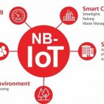
The trend here is no mobility (eg for parking meters or street lights) or very low mobility, with need to send only a few bytes periodically (how often do you need to be reminded “still working and still no car parked at this meter”?). Battery life is incredibly important; maintenance costs to replace batteries, even annually, could undermine the value of the solution. Compute isn’t going to be a big power factor so low-power communication becomes very important. That’s why the Narrow-Band IoT (NB-IoT) standard was developed – to provide a low-power, low-datarate cellular communication solution.
Compared to standard LTE at rates of mega-bits per second, NB-IoT only has to support ~100Kbps, using only a small fraction of the bandwidth. It also can run at much lower power and need only provide half-duplex support. The smaller bandwidth allows for a much smaller RF bill-of-materials (BOM), reduced power means that the RF and power amplifier can be integrated on the same die with the rest of the functionality, and half-duplex further reduces the RF BOM. Together this allows all the communication hardware to be integrated on one die, it provides long-range communication eliminating the need for gateways, and it is reasonable to expect a 10-year battery life.
So far I’ve just talked about the standard (NB-IoT, also known as Release 13, also known as LTE Cat-NB1) because there is an upcoming revision (eNB-IoT, also known as Release 14, also known as LTE Cat-NB2) which I’ll talk about more in a later blog (*). CEVA provides a product to support this standard in their Dragonfly NB1 solution IP. They’re an acknowledged leader in communication IP building on their core DSP strengths, so it’s no surprise that they’re all ready to serve this domain. The solution is built on their X1 core (interestingly designed after the X2, making it a prequel?) and includes digital front-end, RF transceiver, peripherals and software stack. So far, so good – CEVA is helping their customers stay current with evolving communications options.
Where this gets interesting is that the X1 has been designed to function effectively not just as a DSP (for communication) but also as a general-purpose CPU for this domain. X1 has been tuned to deliver competitive performance as a CPU, comparable to Cortex-M4 in Coremark, and provides (they tell me) a compiler-friendly architecture, large orthogonal register file, compact code, full RTOS support, fast context-switch and more. And while M4 provides some DSP instructions for comms support, DSP is CEVA’s home turf so they’re naturally stronger in that area. OK, so X1 has the capability to handle both communication SW and general-purpose software, but won’t it be bogged down in communication when active?
CEVA ran an interesting NB-IoT benchmark, looking at load on the X1 at a typical operating frequency. They found that nearly 50% of the time, the processor was idle. Of course this core can’t run Android and other big workloads, but it doesn’t have to (honestly, if you’re trying to run Android on an NB-IoT device, you have different problems). All you want is to run is some sensor fusion and fairly simple application software. Which it looks like the X1 has plenty of capacity to support.
And that’s just what CEVA wanted – a low-cost single-chip solution for NB-IoT, no need to add a separately licensed MCU core. In fact all you have to add to Dragonfly is embedded flash. They provide all the other logic/interfaces, including cache memory to reduce latency on memory accesses. And they provide all the software. So this solution really can get down to the low unit cost that NB-IoT solution providers need. Naturally they provide a reference solution for all of this.
Emmanuel Gresset (Director Biz Dev in the CEVA Wireless Unit) tells me CEVA believes this has a lot of potential as NB-IoT takes off. Right now, solutions are commonly based around a slim modem (one chip) from a major supplier, plus your own chip to handle your requirements. Bluetooth started with similar multichip solutions, however price-pressures forced integration. The same will happen, perhaps even more so, for NB-IoT apps where pricing expectations will likely be lower still. He added another fascinating point along similar lines. Providers really want to drive solution prices down to the $2-$2.50 range. To do this, they’re looking for ways to reduce stacked margins up and down the supply chain. Some system houses are now partnering with CEVA and ASIC shops to provide the content and expertise to build and manufacture their solutions. Yet another driver of disruption in the supply chain 😎.
You can learn more about Dragonfly-NB1 HERE. You might also want to register for an upcoming related webinar chaired by Daniel Nenni: Custom SoCs for Narrowband IoT (NB-IoT).
(*) Thanks to Emmanuel for corrections to the naming :p