I’m on a mini-roll on the subject of high-level design for ML-based systems. No complaints from me, this is one of my favorite domains and is certainly a hot area; it’s great to that EDA vendors are so active in advancing ML-based design. Here I want to talk about the Catapult HLS flow for use in ML design.
Since I’ve covered the ML topic multiple times, I won’t bore you with a lengthy discourse on the basics. ML (at least in this context) is based on convolutional neural nets (CNNs), inspired (somewhat) by the way neurons process information in our brains, starting from a full image and progressing through transformations in layers of operations with coefficients/weights pre-determined by training to ultimately indicate recognition of a trained image.
From a design point of view, this doesn’t look much like regular logic design/architecture, though of course it all winds up in logic functions, primarily multiply-accumulate (MAC) functions, 4-port registers for tightly-coupled memory and SRAM for next-level caching, all most commonly supporting some type of fixed-point representation. But these are leaf-level functions. The layers in a vision CNN may be processing images with 1M+ pixels, each with 24+ bits for color. So the first layer alone has to process a huge number of inputs (down-sampling through later layers will progressively reduce these sizes).
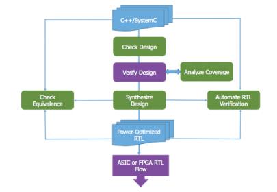
That means you have to use high-level modeling to experiment with architecture choices and to validate your design against real image data. And if you can map your ultimate design to RTL through high-level synthesis (HLS), such as Mentor’s Catapult HLS, so much the better, especially since that tool supports design in straight C++, making it an appealing starting point for people more familiar with algorithms than the intricacies of SystemC (FYI, Catapult HLS also supports SystemC).
Of course if you want to synthesize to a CNN, you’re going to have to accept some limitations on your C++ coding style. For example, you need to use fixed-point data types and you should use fixed-size memory arrays and array indexes, rather than dynamically allocated memory and pointers. Which is not really a problem because you want to do this anyway to reduce power. Mike Fingeroff (HLS Technologist at Mentor) provides guidance (in the white paper link at the end of this blog) on some of the more common areas where you need to adapt.
Taking the HLS path with Catapult HLS offers a number of advantages. The tool can automatically synthesis interface logic (such as AXI4 video stream) based on simple user choices. It will also automatically optimize timing during the synthesis scheduling step, given constraints you set for other factors such as latency and area. In fact in general this is an area where you can experiment with timing versus resource/area tradeoffs based on feedback from the tool. For example you can look at tradeoffs in unrolling loops to drive parallelism. The tool will also help you explore tradeoffs in memory such as word-width and block or interleave choices. And, using PowerPro technology, the tool lets you explore the power implications of all these tradeoffs, so between all these factors you can get to an optimum PPA for your design.
One question occurred to me – how do you bootstrap this process from a trained network with weights? Ellie Burns, Director of Marketing, Calypto Systems Division at Mentor, provided a revealing explanation. It might seem like this is a big deal, but in practice current customers are carrying over the design (and weights) more or less by hand or using their own scripts without difficulty. The much more important need for those teams is the PPA tuning they can get in optimizing microarchitecture choices. Experimenting with options in the synthesis engine and testing/characterizing with real-images/video at the C-level is where they invest the majority of their effort.
Computer vision has become a critical differentiator in many products, but obviously it is not enough that such products support vision. They also need to be fast, very low power and as low cost as possible in many contexts (such as IoT applications). Those are challenging goals; you are adding state-of-the-art functionality but it still needs to fit inside a consumer-acceptable footprint. HLS is an interesting way to get there, by letting you experiment with your algorithm in C++ to optimize and fine-tune the implementation through synthesis. I should add that this flow works both with ASIC-based and FPGA-based designs. You can learn more from this white-paper.