One of the companies I met at ARM TechCon was Dover Microsystems who offer a product in embedded security. You might ask why we need yet another security solution. Surely we’re overloaded with security options from ARM and many others in the forms of TEEs, secure boots, secure enclaves and so on? Why do we need more? Because defending against security breaches is a never-ending battle; no-one is ever going to have the ultimate answer. This is particularly true in software, which is only guarded in the most secure of these systems to the extent that software designers comprehensively consider potential attacks and correctly use whatever memory protection strategies are provided. Given the complexity of modern software stacks, that is not a trivial task.
So how are you going to defend against vulnerabilities you don’t even know exist – the unknown unknowns? Dover have come up with an interesting idea that I like to think of as rather like runtime assertion-based verification (ABV). Think about why we use ABV in hardware design verification. We can’t anticipate everything that might possibly go wrong in a complex system, but we do know that there are certain statements we can make about behavior that should always be true or conversely always false. We have a language in which we can write these assertions (most commonly SVA) enabling us to write our own arbitrarily complex checks. When an assertion triggers in simulation, we trace back in debug and typically find some unexpected combination of conditions we never considered. Even though we hadn’t thought of it, the ABV approach caught it anyway.
I’ve long been a believer that ABV in some form could have value beyond design verification, catching problems at runtime. This could trap potential error conditions, for immediate defensive response and for later diagnosis, leading to software revs to defend against whatever unusual state triggered the problem.
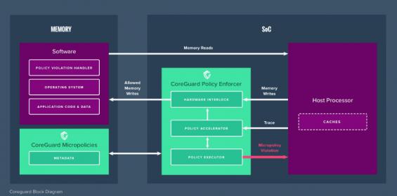
From my perspective, Dover takes an approach along these lines, but instead of assertions being embedded in the mission hardware, they run in a separate IP they call a “policy enforcer” and Dover uses “rules” rather than “assertions” to describe what they check. A collection of rules to check for a class of attacks they call a “micropolicy”. Also they’re not looking at microarchitecture behavior; they’re watching the processor instruction trace and attempted writes to memory, (along with some additional data) which makes sense since they are looking at software-based attacks. They do this in a dedicated processor, sitting to the side of the main processor, so performance impact is limited and attacks on the main processor don’t affect this processor. Nothing is immune from attacks of course but separating this function should make attacks on this monitor more difficult.
In my assertion analogy, the assertions are bit more complex than just direct checks on instructions and addresses. You might build a state table to track where you are in significant aspects of operation flow, also you may choose to label (color) data in different regions. Dover call this information built for and used by the policies “metadata”, which they store in a secured region of the main memory. So when a rule is checking the validity of an operation (say a store), it can check not only the current instruction and target address, but also the metadata. Not too different from the fancy assertions IP verification experts build for protocol checking.
When a policy is violated, the current instruction will not be allowed to complete, and an exception is triggered in the main processor. How this is handled is then up to the kernel/OS. In a package delivery drone for example, an exception might cause the drone to disable network connections, switch into safe mode, load a home GPS location from an encrypted store and fly there.
Dover includes a base set of four micropolicies with product. The read-write-execute (RWX) micropolicy is designed to label regions or even words in memory as readable, writable and/or executable so that operations in violation of this labelling will be caught. The Heap micropolicy is designed is designed particularly to catch buffer-overflow exploits. A pointer to a buffer and the buffer itself (created on a malloc) are colored the same. Attempting to write beyond the upper boundary of the malloc, into a differently-colored region, will trigger a violation. In the Stack micropolicy, stack-smashing attacks which attempt to modify the return address through (compile-time sized) buffer overwrites are prevented. This is conceptually similar to the heap approach but must preserve the integrity of the whole stack.
The fourth base micropolicy is called CFI, for control flow integrity, and is designed to trap code-reuse attacks. These are a variant on return-oriented programming (ROP), where instead of trying to return to an injected malware routine, the code returns to a libc function, such as “system” which can then execute externally-provided malware. The CFI micropolicy profiles locations that contain instructions rather than data and targets/destinations of jumps. This profile cannot be altered during runtime. If a non-tagged location attempts a jump, or a jump is attempted outside the profiled set, the policy will trigger an error.
Dover’s CoreGuard IP integrates with RISC architectures (ARM and RISC-V). The technology originated as part of the DARPA CRASH program in 2010, was incubated by Draper in 2015, and was spun out through Dover as a commercial entity in 2017. The company has now grown to over 20 people and has closed an initial $6 million round of seed funding. Even more impressive, they are working with NXP towards embedding their solution in NXP controllers. You can learn more about the company HERE.