webinar banner AI 2026 v2

Which Way is Up for Lyft, Uber?

Which Way is Up for Lyft, Uber?
by Roger C. Lanctot on 04-07-2019 at 7:00 am

Lyft’s initial public offering was expected to be the biggest tech offering in two years. A public offering is very much like an elevator and everyone getting on the elevator wants to go up. It’s worth noting as the doors open on the Lyft IPO elevator, General Motors is likely to be getting off – and they are not alone.

Why would anyone get off this elevator if the party is upstairs in the penthouse? Probably because Lyft is making the grab for cash long after most of the meatiest global markets have been sewn up. As if to emphasize the point, Uber made an 11th-hour bid for Careem to lock up the Middle East, one of the few remaining under-served and potentially lucrative markets.

There are a couple of reasons to raise cash with a public offering. The most important one is to stimulate growth. In Lyft’s case that can only come from international expansion – a prospect that promises to deepen the financial crater wherein Lyft already resides.

Didi, Yandex, Uber, Ola, Gett. These are the companies that have corralled the largest global ride hailing market opportunities. More importantly, these are the companies that have done battle with the regulators, worked out the licensing, fought off the taxi drivers and established their market presence.

This is no party for a fashionably late arrival. The low hanging fruit has been picked. The battles have been fought. The lessons have been learned.

While Uber has had a tough go of it here and there, conceding China to DiDi, for example, the company has crafted a survival strategy that is already altering market conditions and growth prospects globally. The key to Uber’s strategy – where it has been forced to innovate – has been sub-contracting with existing taxi drivers in markets ranging from the Middle East to Eastern Europe, Scandinavia and Japan.

This go along to get along approach is helping to keep Uber in business – i.e. customers can request an Uber even though it is a taxi that will provide the ride. It has helped keep Uber in play while changing the underlying path to profit.
At least Uber has a path forward. Lyft has nothing but market barriers and an endless vista of loss-producing opportunities. As if to further drive the point home, Uber has reduced driver per-mile compensation in some markets stirring up Uber resentment.

The tweak to compensation only emphasizes the reality that Uber can readily undercut Lyft at any time – especially given how many Lyft drivers are also driving for Uber. At the touch of a button, Uber can have Lyft on its knees in the U.S., while steadily inching its way to profitability overseas.

In spite of this, the Lyft IPO is poised for liftoff. No doubt the early investors, like GM, will cash out along with a mass of insiders. In the absence of a Google or Facebook-like upside these investors will clearly be counting on either an acquisition exit or an autonomous vehicle breakthrough. The prospects of either of these outcomes are slender.
I will happily continue to use Lyft, in the U.S., but I won’t be entering that elevator. Too many people will be getting off the elevator when markets open today. There is wisdom in that decision.



The ESD Alliance Welcomes You to an Evening with Jim Hogan and Paul Cunningham

The ESD Alliance Welcomes You to an Evening with Jim Hogan and Paul Cunningham
by Bob Smith on 04-05-2019 at 7:00 am

An informal “Fireside Chat” like no other featuring Jim Hogan, managing partner of Vista Ventures, LLC., and Paul Cunningham, Cadence’s corporate vice president and general manager of the system verification group, is in the works for Wednesday, April 10.

Hosted by the ESD Alliance, a SEMI Strategic Association Partner, at the SEMI corporate headquarters in Milpitas, Calif., we’re planning plenty of time for networking, dinner and insights from Jim and Paul.

Naturally, Jim and Paul have more than enough to talk about in just one hour-long discussion. Paul’s experiences are varied and include being an entrepreneur as founder and CEO of Azuro. Azuro subsequently was acquired by Cadence in 2011. He now manages Cadence’s system functional verification activities, after moving from physical design tools development 18 months ago.

Attendees can expect to hear about the verification challenges ahead, as well as open source architectures and the necessary development platforms. Paul previously worked in artificial intelligence before it was an industry trend and may be asked about this as well.

The evening begins at 6:30pm with dinner and runs until 9pm. SEMI is located at 673 S. Milpitas Boulevard in Milpitas, Calif., and has ample free parking.

Everyone from the electronic system and semiconductor design ecosystem is welcome to attend. It is open free of charge to all ESD Alliance and SEMI member companies. Non-members and guests can attend for a fee of $40. Registration information can be found at: https://bit.ly/2Ot4azb

Please plan to join us and bring your questions or observations. Be sure to ask us about our newest initiative ES Design West co-located with SEMICON West 2019 July 9-11 at San Francisco’s Moscone Center South Hall.

About Jim Hogan and Paul Cunningham
Jim Hogan doesn’t really need an introduction from me. He is well-known as an experienced senior executive and tireless advocate for our electronic system and semiconductor design ecosystem who has worked in the semiconductor design and manufacturing industry for more than 40 years. Jim currently serves as a board director for electronic design automation, intellectual property, semiconductor equipment, material science and IT companies.

Paul Cunningham’s product responsibilities at Cadence include logic simulation, emulation, prototyping, formal verification, Verification IP and debug. Previously, he was responsible for Cadence’s front-end digital design tools, including logic synthesis and design-for-test. Cunningham joined Cadence through the acquisition of Azuro, a startup developing concurrent physical optimization and useful skew clock tree synthesis technologies, where he was a co-founder and CEO. He holds a Master of Science degree and a Ph.D. in Computer Science from the University of Cambridge, U.K.

About the Electronic System Design Alliance
The Electronic System Design (ESD) Alliance, a SEMI Strategic Association Partner representing members in the electronic system and semiconductor design ecosystem, is a community that addresses technical, marketing, economic and legislative issues affecting the entire industry. It acts as the central voice to communicate and promote the value of the semiconductor design ecosystem as a vital component of the global electronics industry. Visit www.esd-alliance.org to learn more.


Google Stadia is Here. What’s Your Move, Nvidia?

Google Stadia is Here. What’s Your Move, Nvidia?
by Krishna Betai on 04-04-2019 at 12:00 pm

On March 16, 2019, Google introduced the world to its cloud-based, multi-platform gaming service, Stadia. Described as “a gaming platform for everyone” by Google CEO Sundar Pichai at the Game Developers Conference, Stadia would make high-end games accessible to everyone. The video gaming industry, as we know it, will never be the same again.

Google executive Phil Harrison explained that Stadia will not require expensive gaming consoles and hardware; all necessary updates to the games and the platform would be made remotely on its data centers. Furthermore, Stadia will enable gaming on multiple devices — laptops, desktop computers, smartphones, tablets, and smart TVs via Chromecast at a resolution of 4K at 60fps (which Google will eventually bump up to 8K). A user can start playing on one device and resume playing on any other, so as to maintain continuity, a feature that was seen on the Nintendo Switch. As Harrison enlisted the new platform’s many features, including an exclusive Stadia controller, he announced Google’s partnership with AMD to build a custom GPU for the platform. With AMD at the core of the PlayStation and the Xbox gaming consoles, and now Google Stadia, all sorts of questions arise on the impact of Google’s new platform on Nvidia, the former’s biggest rival.

Nvidia’s answer: its cloud-based gaming platform, GeForce Now.

Nvidia, famous for its gaming hardware and its high-quality graphics cards, has become a home for hardcore PC gamers. While AMD is one up in the gaming console space, Nvidia is unbeatable when it comes to desktop computers and laptops. However, its dominance in the PC space is under potential threat from Google Stadia.

Like Stadia, GeForce Now does not require dedicated gaming hardware or massive software downloads. Moreover, GeForce Now has been in the market for over a year now, in beta mode. Nvidia boasts of more than 300,000 existing beta users of GeForce Now, as the waitlist to try it out crosses the one million mark. At Nvidia’s GPU Technology Conference, Nvidia CEO Jensen Huang proudly claimed the arrival of “ray tracing” in gaming, a technique that was used only in animated films before. Ray tracing is the process of creating an image by tracing the path of millions of simulated lights, thereby recreating the effects of light in real-life, on the screen. As games get incredibly detailed over the years, light plays an important role in the overall gameplay. To create the effects of lights and shadows on a screen is painstaking, but Nvidia’s new RTX GPU makes that process simple. Developers would be able to make light interact with different objects with ease — changing hues and creating shadows will become easy, accurate, and done in real-time. Huang was optimistic about integrating RTX to GeForce Now servers by the second or third quarter of 2019, which would attract a lot of game developers and gamers.

While Google aims to attract even casual gamers to play AAA games (games with high-end graphics) with Stadia, Nvidia looks to provide an enthusiast-level gaming experience to those who do not have the resources to do so. While analysts have labelled Stadia to be the “Netflix for gaming,” Huang does not believe in that economic model, as far as gaming is concerned. The choice of games, according to him, is based on peers. A gamer is more likely to play the same game as their friends, rather than a random game from a vast library of games.

Google Stadia will be powered by custom-made AMD GPUs. However, Nvidia is confident in its indigenous hardware to tackle its rivals. Even though AMD announced its new 7nm Radeon graphics chip, Huang claimed that the build, quality, and engineering of Nvidia’s 12nm Turing architecture-based chip would supersede the former in performance and efficiency. Unlike traditional client-server-based platforms, on Stadia, both the gamer and game server are connected via Google’s network, thus ensuring reliable connectivity, low latency, and the best gaming experience across a large number of players.

With 5G around the corner, Nvidia is confident about the performance of GeForce Now when the new network comes into the wild. The company has already joined hands with SoftBank Corporation in Japan, and LG Uplus in South Korea to expand cloud gaming globally. Gaming on GeForce Now with a 5G network on a non-gaming laptop ensured a lag of only 16 milliseconds; anything below 60ms meant optimal gaming experience, according to Nvidia. As 5G becomes widely available, it hopes to bring this lag down to 3ms.

The only hurdles on Nvidia’s path to game streaming are the internet speed and Google’s widespread, powerful data centers. While GeForce Now will not run on Nvidia’s own servers, but on the servers of the respective game developers, Nvidia is banking on the upcoming 5G technology and its partnerships with different telecommunication companies to tackle these issues.

Gaming is child’s play, one might think. but the $137.9 billion gaming industry suggests that it is much more. The announcement of Google Stadia is indicative of the direction that the gaming industry is headed toward. The AMD-powered Stadia could spell doom for Nvidia, but not yet. Google has kept the pricing and the games available under the service under wraps. Nvidia, a household name among game enthusiasts, is relying on the trustworthiness of the GeForce brand name, ray tracing, and the advent of 5G technologies for the success of its platform. Hopefully, the game streaming wars will be as fun as gaming itself.


So What is Quantum Computing Good For?

So What is Quantum Computing Good For?
by Bernard Murphy on 04-04-2019 at 12:00 am

If you have checked out any of my previous blogs on quantum computing (QC), you may think I am not a fan. That isn’t entirely correct. I’m not a fan of hyperbolic extrapolations of the potential, but there are some applications which are entirely sensible and, I think, promising. Unsurprisingly, these largely revolve around applying QC to study quantum problems. If you want to study systems of superpositions of quantum states, what better way to do that than to use a quantum computer?

The quantum mechanics you (may) remember from college works well for atomic hydrogen and for free particles used in experiments like those using Young’s slits. What they didn’t teach you in college is that anything more complex is fiendishly difficult. This is largely because these are many-body problems which can’t be solved exactly in classical mechanics either; quantum mechanics provides no free pass around this issue. In both cases, methods are needed to approximate; in the quantum case using techniques like the Born-Oppenheimer approximation to simplify the problem by effectively decoupling nuclear wave-functions from electron wave-functions.

As molecules grown in size techniques become progressively more sophisticated, one frontier of which today is represented by something called density functional theory with (for our domain) the confusing acronym DFT. Whatever method is used, all these techniques require a compounding pile of approximations, all well-justified, but leaving you wondering where you might be missing something important. Which is why quantum chemistry depends so heavily on experiment (spectroscopy) to provide the reality against which theories can be tested.

But what do the theorists do when the experimentalists tell them they got it wrong? Trial-and-error is too expensive and fitting the theory to the facts is unhelpful, so they need a better way to calculate. That’s where QC comes in. If you have a computer that can, by construction, accurately model superpositions of quantum states then you should (in principle) be able to model molecular quantum states and transitions.

The Department of Energy, which had long steered clear of the QC hype, started investing last year to accelerate development along these lines. They mention understanding the mechanism behind enzyme-based catalysis in nitrogen-fixing as one possible application. Modeling matter in neutron stars is another interesting possibility. Lawrence Berkeley Labs has received some of this funding to develop algorithms, compilers and other software, and novel quantum computers in support of this direction in analytical quantum chemistry.

Meanwhile, a chemistry group at the University of Chicago are aiming to better understand a phenomenon, grounded in the Pauli exclusion principle, in this case applying in >2 electron systems, which are known as generalized Pauli constraints. As a quick refresher, the Pauli exclusion principle says that two electrons(/fermions) cannot occupy exactly the same quantum state. The generalized constraints add further limits in systems with more than 2 electrons. The mechanics of this methods seem quite well established though far from universally proven, and the underlying physics is still in debate. Again, QC offers hope of better understanding that underlying physics.

A word of caution though. Modeling a system with N electrons will almost certainly require more than N qubits. Each electron has multiple degrees of freedom in the quantum world – the principal quantum number, angular momentum and spin angular momentum at minimum. And there’s some level of interaction of each of these with the nucleus. So a minimum of 6 qubits per electron, multiplied by however many qubits are needed to handle quantum error correction. Probably not going to be seeing any realistic QC calculations on proteins any time soon.


My Thoughts on Cadence in the Cloud

My Thoughts on Cadence in the Cloud
by Daniel Nenni on 04-03-2019 at 12:00 pm

The cloud is a highly popular term that a lot of people don’t fully understand. If you are one of those people please read on as I will share my experience, observations, and opinions. Even if you are a cloud aficionado you may want to catch up on what’s new with EDA cloud services so again read on.

When we first started SemiWiki 9 years ago we chose a host with what was called a virtual server. The hosting company was an expert on applications based on the MySQL database software which made it an easy choice for us since we were first time cloud residents. A virtual server is something we shared with others that also promised scalability for future growth. SemiWiki quickly exceeded expectations so our host migrated us to a private cloud server that we continued to upgrade.

Recently we moved SemiWiki 1.0 to one of the top three cloud providers for improved bandwidth, uptime, and scalability as SemiWiki 2.0 is coming soon with a couple of big surprises. Moving from a private cloud to a public one was a lot less trouble than one might expect. It was like removing Band-aids versus having cosmetic surgery. Cloud pricing thus far is significantly less for us and the available cloud tools, scalability, and the additional security opens up a whole host of business opportunities for SemiWiki, absolutely.

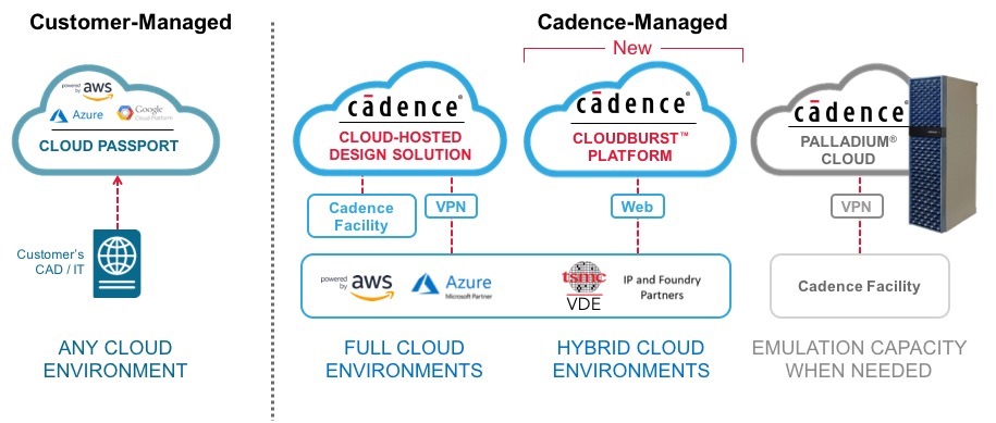
Cadence has been in the cloud for many years starting with Virtual CAD (VCAD) more than 20 years ago, Hosted Design Solutions (HDS) 10 years ago, and the Cadence Cloud announcement last year with TSMC, Amazon, Microsoft, and Google as partners. Yesterday they announced the Cloudburst Platformwhich is another important EDA step towards full cloud implementation. So please give credit where credit is due, Cadence is THE EDA cloud pioneer and that will continue.

At CDNLive I had another chat with Craig Johnson, VP of Cloud Development, for a Cadence cloud update. Craig is a no-nonsense guy who will answer your questions straight up. Craig started his career with 10+ years at Intel and has been at Cadence for almost 15 years. Cloud adoption is still ramping up but remember, Cadence has been working towards this for more than 20 years so you won’t find a better EDA cloud partner. For me the EDA cloud question is not IF, it is WHEN, if we want better chips faster for continued semiconductor industry growth.

Here is the relevant verbiage from the press release:

The Cadence CloudBurst platform enables companies of all sizes to build upon the standard benefits of the broader Cadence Cloud portfolio—improved productivity, scalability, security and flexibility—with a deployment option that delivers a hybrid cloud environment in just a day or two after initial purchase versus the typical timeframes for internally provided cloud solutions that can take weeks to deploy. It offers customers a production-proven, Cadence-managed environment for compute-intensive EDA workloads with no tool installation or cloud set-up required so that engineers can stay focused on completing critical, revenue-generating design projects.

Additional benefits systems and semiconductor companies can achieve with the Cadence CloudBurst platform include:

  • Ability to address today’s design challenges:The platform provides convenient and secure browser-based access to the scale of cloud computing options and includes unique file-transfer technology that significantly accelerates the transfer speed of the massive files created by today’s complex system-on-chip (SoC) designs
  • Ease of deployment:The platform complements existing on-premises datacenter investments and enables CAD and IT teams to easily address peak needs by providing a hybrid environment without requiring prior cloud expertise
  • Access to a broad set of Cadence tools:The platform supports a range of cloud-ready tools including functional verification, circuit simulation, library characterization and signoff tools, which benefit from cloud-scale compute resources
  • Streamlined ordering process:Customers can utilize existing ordering and licensing systems, eliminating sometimes lengthy legal and administrative hassles so customers can begin using the cloud for design projects quickly

“Our vision is to continuously evolve our cloud offerings to remove barriers to adoption and make customers successful in their shift to the cloud regardless of legacy investments or level of cloud experience,” said Dr. Anirudh Devgan, president of Cadence. “By adding the CloudBurst platform to our Cadence Cloud portfolio, we’re providing customers with an unparalleled offering for hybrid cloud environments, which lets customers harness the full power of the cloud for SoC development.”

The broader Cadence Cloud portfolio consists of the new CloudBurst platform as well as the customer-managed Cloud Passport model and the Cadence-managed Cloud-Hosted Design Solution and Palladium ® Cloud solutions. The Cadence-managed offerings provide customers with solutions that fully support TSMC’s Open Innovation Platform Virtual Design Environment (OIP VDE). The portfolio offerings support the broader Cadence System Design Enablement strategy, which enables systems and semiconductor companies to create complete, differentiated end products more efficiently.

Endorsements
“We successfully ran more than 500 million instances flat using the fully distributed Cadence Tempus Timing Signoff Solution on the CloudBurst platform via AWS to complete the tapeout of our latest TSMC 7nm networking chip. This would have been impossible to achieve in the required timeframe if we hadn’t deployed the Cadence hybrid cloud solution, which offered quick and easy access to the massive compute power we needed and a 10X productivity improvement over an on-premises static timing analysis approach for final signoff.”
-Dan Lenoski, chief development officer and co-founder, Barefoot Networks

“Optimizing a cloud architecture to support heavy-duty EDA workloads has been TSMC’s primary focus for delivering cloud-ready design solutions to customers jointly with our Cloud Alliance partners. This new offering from Cadence has met TSMC’s goal of the OIP VDE simplifying cloud adoption and demonstrated its ability to provide innovative service to our mutual customers with secure access to a simple-to-create, cloud-based environment that allows cloud bursting for peak needs, as well as accelerated completion of specific functions including simulation, signoff and library characterization without the typical challenges associated with hybrid cloud use models. We’re already seeing customers achieve productivity gains and look forward to seeing many more successes.”
-Suk Lee, senior director of Design Infrastructure Management Division, TSMC

“More IC design companies are choosing to host their entire EDA workload in the cloud, but companies who have large datacenters at the core of their compute infrastructure may find hybrid cloud environments as a compelling starting point in their journey to the cloud. By utilizing the Cadence CloudBurst platform, customers can easily leverage the scale of Microsoft Azure in order to meet their peak capacity requirements, thereby speeding up the time-to-market for their complex designs.”
-Rani Borkar, corporate vice president, Microsoft Azure


Solving the EM Solver Problem

Solving the EM Solver Problem
by Tom Simon on 04-03-2019 at 7:00 am

The need for full wave EM solvers has been creeping into digital design for some time. Higher operating frequencies – like those found in 112G links, lower noise margins – caused by multi level signaling such as in PAM-4, and increasing design complexity – as seen in RDL structures, interposers, advanced connector and long reach connections, all call for EM analysis. Existing EM solvers are extremely difficult to set up and have runtimes and memory requirements that increase exponentially as design complexity increases.

Designers have resorted to partitioning and simplifying designs so that they become manageable for solver runs. However, partitioning the designs to make it feasible to run EM solvers leaves important interactions out of the analysis. This means that EM solver performance and capacity issues are limiting their widespread use.

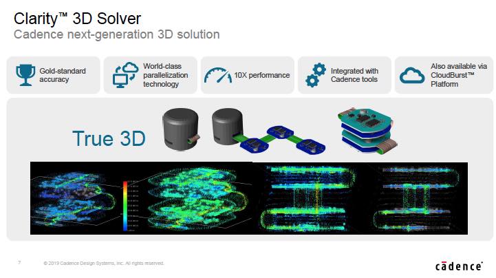
Cadence has just announced a new product called Clarity that looks as though it can address the EM simulation requirements of today’s complex high speed systems. Clarity is the first product from Cadence’s new System Analysis Group. Front and center in their announcement is an example of a 112G interconnect. Clarity can digest whole each of the complex elements in such as system.

At each end of the 112G data link is the redistribution layer (RDL) of thick metal carrying the signal to package connections. While RDL is relatively planar, it’s wide and thick metal calls for a full 3D solver. Packages contain balls, bumps. vias and complex routing, which are also difficult for many solvers. Likewise, PCBs have many layers with vias, pad stacks and other 3D elements. Connectors, cables and backplanes all have become complex and are subject to high frequency electromagnetic effects.

This new solver from Cadence boasts much higher capacity and performance. They have added a parallel execution capability that allows it to use large arrays of distributed processors and it also has support for HPC. Typically, designers were frustrated with existing solvers because the analysis problem would simply become to large to run on any machine. Cadence says that the Clarity solver can scale up to handle larger designs with virtually no limits. They cite its ability to use hundreds of processors in parallel.

On the performance side, Cadence points to two different test cases where scaling the number of processors improved runtime by over 10X. The first case is a 112G connector-PCB interface, where they scaled from 40 CPUs to 320. They saw a 12.3X improvement in runtime. Though this is a large number of CPUs, it speaks to the parallelism they are promoting. The second case is a DDR4 interface. In going from 40 to 320 processors, they see a 10.4X improvement in runtime.

Cadence says that Clarity can easily be used as part of an optimization flow, to help solve difficult design challenges. Clarity is integrated with the Sigrity 3D Workbench, making it much more than just an analysis point tool.

Their announcement includes endorsements from Teradyne and HiSilicon. From the comments those companies have made, it is clear that the performance and capacity improvements are meaningful. It seems that a tool like Clarity is the departure point for much more comprehensive EM analysis in a wide variety of systems. EM effects, by their very nature, are spread across multiple elements in a system. One simulation result Cadence showed was of a set of boards with flexible flat ribbon cables folded over and placed in a compact housing.

New designs running at what was once considered exotic mm-wave frequencies are becoming essential for new products that meet the demanding requirements for data centers, automotive, communications and other key areas. EM solvers are moving from being a niche tool to one that is going to be required frequently to build these complex products. In many ways, up until now the major players in EDA have left EM solvers to smaller point tool vendors. The announcement of their new Clarity solver should be seen as a sign that this is changing and that solvers are now considered a key enabling technology. Cadence seems to have made good use of their significant development resources to make major improvements in a very complex product area.


What to Expect from the GSA Executive European Forum?

What to Expect from the GSA Executive European Forum?
by Eric Esteve on 04-02-2019 at 7:00 am

I plan to attend to the GSA European Forum in Munich (April 15-16), so I first looked at the event description and at the impressive speakers list. In such event, the goal is at 50% to listen, and 50% to network with the speakers and the other attendant. The center of gravity is clearly semiconductor, but the event involved speakers from all the ecosystem around the semi industry.

We can start by naming the semiconductor heavyweights, Samsung, Infineon, TSMC, ST Micro, NXP or ON Semi, but it’s interesting to notice that their customers are also part of the speakers. We are in Munich, a place where the automotive industry is part of the land DNA, so it’s not surprising to see that BMW, Robert Bosch or Continental will participate.

And also, AImotive (founded in 2015, the company target autonomous level 5) and Smart Eye (developing solutions based on eye tracking technology to address safety related needs in automotive) or AnotherBrain (who has created a new kind of artificial intelligence, called Organic AI) targeting automotive, industrial automation and some IoT.

The networking industry is well represented with speakers from Nokia Mobile Networks, Mellanox and Huawei. This Chinese company help bridging with the service part of the ecosystem, with another well-known company, Canyon Bridge, a Chinese fund with HQ in the Silicon Valley.

I rank in the service category the EDA big 3, Cadence, Mentor and Synopsys and I realize that Soitec is providing SOI wafer, another kind of service, but rather hardware! HIS Markit and Mc Kinsey will be part of the speakers too.

You can register to the GSA Forum here, or just take a look so you will have the opportunity to read this abstract:

This year, we’re focusing the conversation on how to best take advantage of unprecedented opportunities that are available to us today – AI, Automotive, IoT, 5G, High Performance Computing, Cloud, AR/VR, etc. – while darker clouds seem to be appearing on the horizon: trade wars & tariffs, signs of industry inventory buildups and of a slowing Chinese economy. And at the same time with the industry ecosystem shifting and expanding, blurring the lines between semiconductors, software, services, solutions and systems.

Thanks to Sandro Grigolli from GSA, I could have a look in advance to a couple of presentations that were recently delivered internally to the GSA board on two topics that will be presented also at the European Executive Forum in Munich. I don’t want to spoil the event, so I have just extracted two slides from Canyon Bridge presentation “China Semiconductor Market Overview”, that I find extremely informative about “China Goals” and “Fab capacity in China”.

The GSA Executive Forum is clearly networking oriented, but the quality of some presentations make it closer of a geopolitical conference than just a pure marketing event.

Eric Esteve from IPnest


Moore’s Law extended with new "gateless" transistor

Moore’s Law extended with new "gateless" transistor
by Robert Maire on 04-01-2019 at 10:00 am

Micron Buries the Hatchet with China
Micron has a very long history of counter cyclical investing, buying the assets of vanquished competitors when the memory industry is at the bottom of the cycle, such as it is right now.

Over the weekend, Micron announced that it had an agreement to acquire the assets of the now stalled Jinhua memory fab in China. Concurrent with the acquisition agreement, the Chinese government will lift all current restrictions on Micron in China now that Micron will be manufacturing memory devices in China.

The fab which Jinhua built in China has been stalled since the US government ordered US equipment makers to stop doing business with Jinhua, similar to what happened to ZTE. This means that after spending several billion dollars building the fab it became essentially useless after US equipment companies such as Applied Materials, Lam, KLA and even Dutch ASML pulled out in a hurry. Although the purchase price was not reported in the press release, we would speculate that Micron paid pennies on the dollar (or yuan) for the idled assets.

Micron CEO comments
Micron’s CEO Sanjay Mehrota commented on the proposed transaction, “This deal is very compelling as it accomplishes many things for Micron. It gets us new capacity, in a rapidly growing market, China and it puts an end to all of our legal restrictions in China. We were also able to obtain these assets at a very attractive price given their current under-utilization” , Sanjay added ” We are quite pleased with the fab as it has the exact set of tools needed for Micron’s process. In addition the fab is physically laid out just like Micron’s Taiwan fab including the software infrastructure”

As part of the agreement the US government will unblock sales to the former Jinhua fab which we are sure the current administration will position as a big win, for the US, much as the agreement to restart sales to ZTE.

KLA Kosher Konversion
Following the closing of KLA’s recent Orbotech acquisition, the company announced that it would be changing its corporate domicile from the US to Israel for a number of reasons. Post the Orbotech close, KLA, which already had substantial operations in Israel, became one of the largest tech companies in Israel. Israel’s “Office of the Chief Scientist” which is responsible for fostering technology in the country offered KLA several hundred million dollars of financial grants and development loans and in addition offered 10 years of tax abatements if KLA would move its corporate headquarters to Israel and commit to further expansion. Israel, most recently offered hundreds of millions of dollars of incentives to Intel for building is newest 10NM fab there. Israel’s announced deal with KLA would go even beyond that.

KLA, which has a history of creative finance, commented on the deal with CFO Bren Higgins saying, ” Aside from the obvious strong direct financial benefit for KLA shareholders we also see benefit for KLA customers as an Israeli company as many of our products whose sale may have been restricted as a US based company will be freed up to to sell to rapidly emerging markets such as China.” Higgins went on to say, “We had already seen evidence of China reducing US purchases of equipment in reaction to trade concerns, this will remove that barrier” .

The deal which had been negotiated during the long gestation period of the Orbotech deal was also a strong factor in China’s final approval of the deal as China would get more access to KLA product. The secret discussions even had a code name inside the company called “project K” (for Kashering).

IBM new transistor design supports Moore’s Law
The semiconductor industry has wrestled with transistor design to enable a continuation of Moore’s Law by allowing further shrinkage of the basic transistor dimensions. The industry started with “Planar” transistors, then at 22NM went to “FINFETs” (Fin shaped field effect transistor) and most recently GAA (Gate All Around) which shrinks the dimensions even further.

IBM’s research group has announced a GBG (euphemistically call “gate be gone” ) which eliminates the need for a gate which radically reduces the dimensions of the new device. Some in the industry are dismissing IBM’s announcement as nothing more than a “rehash” of prior designs of PINFED’s (Pin field effect diodes)

Saranicle is new pellicle material with 95% EUV transmission
Dow Chemical is said to be working with ASML to solve the vexing pellicle problem which is hampering the roll out of EUV. The new material is a polyvinylidene chloride (PVDC) which makes for a thin flexible membrane. In addition to the high, 95%, EUV transmission factor, which is well above today’s 85%, the material also offers significant mechanical benefits. Old pellicle’s were glued to the mask which produced “outgassing” as the pellicle heated. ASML’s recent “clip” pellicle attachment also had problems as the clips generated particle contamination. Saranicle “clings” through electrostatic forces to the mask eliminating the need for glues or clips.

Versum moves listing from NYSE to Ebay
Versum, a New York stock exchange listed company (ticker VSM), has been stuck in a “tug or war” between Entegris and Merck, both looking acquire the company. Merck has recently gone “hostile” announcing an unsolicited $5.9B or $48 per share versus Entegris’s roughly $39 stock offer. Versum decided it was in the best interest of shareholders to move their stock listing from the NYSE to Ebay in order to facilitate the bidding process. The new Ebay listing has a $100 a share, “buy it now” option.

The Stocks

New memory based ETF starts trading as “MEM”
Given that commodity DRAM and NAND memory pricing has been the underlying driver of many of the chip stocks, equipment companies, semiconductor ETFs as well as the Philadelphia Stock index ( the “SOX”), it was only a matter of time before a direct ownership memory based ETF popped up. Similar to the “GLD” ETF which holds actual gold bullion in various repositories around the world the MEM ETF will stock pile actual memory chips of ranging types and capacities from DRAM to NAND. The Chicago exchange also announced options and futures trading based on the MEM ETF which will also start trading today.

If you haven’t gotten it by now….Happy April First!!


FPGA Landscape Update 2019

FPGA Landscape Update 2019
by Daniel Nenni on 04-01-2019 at 7:00 am

In 2015 Intel acquired Altera for $16.7B changing one of the most heated rivalries (Xilinx vs Altera) the fabless semiconductor ecosystem has ever seen. Prior to the acquisition the FPGA market was fairly evenly split between Xilinx and Altera with Lattice and Actel playing to market niches in the shadows. There were also two FPGA startups Achronix and Tabula waiting in the wings.

The trouble for Altera started when Xilinx moved to TSMC for manufacturing at 28nm. Prior to that Xilinx was closely partnered with UMC and Altera with TSMC. UMC stumbled at 40nm which gave Altera a significant lead over Xilinx. Whoever made the decision at Xilinx to move to TSMC should be crowned FPGA king. UMC again stumbled at 28nm and has yet to produce a production quality FinFET process so it really was a lifesaving move for Xilinx.

In the FPGA business whoever is the first to a new process node has a great advantage with the first design wins and the resulting market share increase. At 28nm Xilinx beat Altera by a small margin which was significant since it was the first TSMC process node Xilinx designed to. At 20nm Xilinx beat Altera by a significant margin which resulted in Altera moving to Intel for 14nm. Altera was again delayed so Xilinx took a strong market lead with TSMC 16nm. When the Intel/Altera 14nm parts finally came out they were very competitive on density, performance and price so it appeared the big FPGA rivalry would continue. Unfortunately, Intel stumbled at 10nm allowing Xilinx to jump from TSMC 16nm to TSMC 7nm skipping 10nm. To be fair, Intel 10nm is closer in density to TSMC 7nm than TSMC 10nm. We will know for sure when the competing chips are field tested across multiple applications.

A couple of interesting FPGA notes: After the Altera acquisition two of the other FPGA players started gaining fame and fortune. In 2010 MicroSemi purchased Actel for $430M. The initial integration was a little bumpy but Actel is now the leading programmable product for Microsemi. In 2017 Canyon Bridge (A Chinese backed private equity firm) planned a $1.3B ($8.30 per share) acquisition of Lattice Semiconductor which was blocked after US Defense officials raised concerns. Lattice continues to thrive independently trading at a high of more than $12 per share in 2019. Given the importance of programmable chips, China will be forced to develop FPGA technology if they are not allowed to acquire it.

Xilinx of course has continued to dominate the FPGA market since the Altera acquisition with the exception of the cloud where Intel/Altera is focused. Xilinx stock was relatively stagnate before Intel acquired Altera but is now trading at 3-4X the pre-acquisition price.

Of the two FPGA start-ups, both of which had Intel investments and manufacturing agreements, Achronix was crowned the winner with more than $100M revenue in 2018. Achronix originally started at Intel 22nm but has since moved to TSMC 16nm and 7nm which will better position them against industry leader Xilinx. Tabula unfortunately did not fair so well. After raising $215M in venture capital starting in 2003 Tabula officially shut down in 2015. They also targeted Intel 22nm and according to LinkedIn several of the key Tabula employees now work for Intel.

According to industry analysts, the FPGA market CAP broke $60B in 2017 and is expected to approach $120B by 2026 growing at a healthy 7% CAGR. The growth of this market is mainly driven by rising demand for AI in the cloud, growth of Internet of Things (IoT), mobile devices, Automotive and Advanced Driver Assistance System (ADAS), and wireless networks (5G). However, the challenges of FPGAs directly competing with ASICs continues but at 7nm FPGAs will have increased speed and density plus lower power consumption so that may change. Especially in the SoC prototyping and emulation markets which are split between ASICs and FPGAs.


Lyft Uber and Soylent Green

Lyft Uber and Soylent Green
by Roger C. Lanctot on 03-31-2019 at 10:00 am

23223 lyft uber soylent green

It wasn’t enough that Lyft and Uber introduced the world to the concept of taxi and limousine drivers committing suicide, we now have Lyft and Uber drivers committing suicide. In other words, it’s not enough that the business models of these companies are suicidal, they are actually visiting suicide upon their non-employees.


SOURCE: Opening scene from “Soylent Green”​

But what if the business model isn’t about providing transportation? What if the real objective of Uber and Lyft is population reduction – like Soylent Green?

Terrifying and saddening though it may be to see taxi and limousine drivers commit suicide after finding – post-Uber/Lyft – that they could no longer afford to pay off either their expensive taxi medallions or their vehicles or their mortgages, it was nevertheless understandable. It was even understandable when drivers for Uber in India committed suicide after Uber over-promised regarding their likely compensation causing some of these drivers to over-commit to buying new cars.

The reason the drivers in India suddenly found themselves in a financial bind was that Uber over-recruited drivers tilting the driver-demand balance toward an unbearable compensation level for the drivers. By the time the drivers realized their quandary, it was too late. That experience was several years ago, but now we are seeing Lyft drivers in the U.S. committing suicide in the midst of a heated battle over a regulation requiring that Lyft pay drivers a minimum wage.

Lyft is resisting the implementation of the new regulation in New York after the negative impact the minimum wage had on fares – driving them up and driving away passengers. As reported in TechCrunch: “These rules legally went into effect in February. Since then, Lyft says there has been a negative impact on driver earnings. That’s because, Lyft says, the cost for passengers increased 24%, which led to rides dropping 26% and driver earnings dropping 15%. Lyft had to then take “action to stabilize the market largely through the use of passenger discounts. We won’t do this forever, but knew it was important for both the driver community and Lyft while the lawsuit progressed.”

No doubt Lyft also reduced fares to maintain market share in the face of closer scrutiny in advance of its initial public offering. The bottom line is that the New York minimum wage requirement was the last Jenga block the removal of which brought down the Lyft-Jenga tower.

The simple reality is that Lyft and Uber can’t afford to pay drivers a minimum wage or the entire business model collapses. But maybe that’s not the purpose of Uber and Lyft and Ola and Yandex and Gett. Maybe the entire purpose of these services is to reduce surplus population.

Imagine a distopian present where there is a surplus of drivers in a world that is shifting toward driverless cars and mass transportation. Government organizations, given the task of reducing the growing ranks of this restive population, cook up a scheme to put more of them in the business of providing ad hoc transportation than the market can bear.

Soon packs of roving “drivers” begin derailing trains and running over bike and scooter users in order to drive more business into their itinerant taxis. Before long, demand for cars begins to grow again as non-drivers see the error of their ways and get back in cars – either their own or as Lyft and Uber passengers. This, of course, exacerbates the driver surplus problem with Purge-like consequences as mayhem ensues.

Suicides committed by taxi and limousine drivers – even one – ought to have been enough to open the eyes of regulators and legislators to the inequity and untenability of ride hailing in its current form across the world. The fact that ride hailing drivers – even one – might have committed suicide ought to have been the final straw. The business model simply does not hold water. There is no alternative revenue track like in-vehicle search or advertising that is sufficient to replace existing driver compensation structures. Lyft has become Soylent Green.

There is one path out of this transportation network company-driven mess. One company has solved this riddle and is fighting for its non-profit corporate life. Ride Austin is a TNC non-profit in Austin that thrived in a post-Uber/Lyft environment before the two companies were allowed back into the local market last year. It just may be that the ride hailing business was intended to be a non-profit proposition. Don’t tell that to Lyft investors.