webinar banner AI 2026 v2

Lyft & Auto Industry Annihilation

Lyft & Auto Industry Annihilation
by Roger C. Lanctot on 03-31-2019 at 5:00 am

The good news is that Lyft’s initial public offering is over-subscribed, according to published reports. That also happens to be the bad news.

Like its disruptive corporate kin – Waymo, Uber, and Tesla Motors – Lyft is out to creatively destroy the automotive industry. In the process, the company is set on a course for its own annihilation – and investors appear more than happy to speed the company along to its own doomed demise.

Car ownership is in the crosshairs of Lyft, Uber and most other ride hailing providers. They have repeatedly announced their intention to separate their customers from their cars. Of course, they draw their drivers from this same population, so this proposition in itself is somewhat self-annihilating.

Car ownership is not the only target of Lyft’s destructive inclinations. Lyft, like Uber and other ride hailing companies, is out to damage or destroy the rental car and the taxi and limousine industries – to say nothing of the negative impact on public transportation (Why take the bus/train/tram?). More recently, during the IPO road show, senior Lyft executives have announced their intention to take on the insurance industry.

One of Lyft’s bigger objectives, though, is to eliminate drivers by mastering automated driving. The company has also invested in scooters and bike sharing – both of which are taking business away from its own ride hailing service.

This fits in nicely with the broader trends in the automotive industry which is set on a path toward electrification, autonomous driving and the proliferation of mobility services. Electrification – and the massive billion-dollar investments that it entails – threatens to wipe out massive swathes of the automotive supply chain even as it demands a colossal and expensive expansion of of charging networks.

Electrification also threatens car dealer networks – at least those, in particular, that are dependent upon the servicing of ICE-based vehicles. Autonomous vehicles, like ride hailing, will eliminate the need for car ownership, as will mobility services. Car makers are heavily investing in these value propositions as well.

As if this automotive industry implosion weren’t enough, the President of the United States continues to be something of a one-man wrecking ball thrashing through the industry. The latest report on the administration’s activities suggests the makings of an escalated tariff war intended to erect barriers at U.S. borders certain to simultaneously make new cars more expensive while stimulating retaliatory tariff strikes against U.S. car makers.

https://tinyurl.com/y5g9tg9t – Trump Administration withholds Report Justifying ‘Shock’ Auto Tariffs – politico.com

Lyft is not the cause of all of this self-destructive mayhem. It is only the most visible and immediate manifestation.
Investors are enthusiastic about Lyft. Are there skeptics? Yes, many. Take Nicholas Farhi, a partner at OC&C strategy consultants quoted in the Washington Post: “The endgame you need to believe is so implausible in my mind – it’s definitely at the ‘hypiest’ end of the unicorns. It’s hard for me to think of a rational reason why people would invest in this.”

Tiernan Ray, writing for TheStreet.com, took issue with Lyft’s creation of what it calls “contribution” – a figure which strips out all operating expenses to disingenuously suggest an improving financial picture for Lyft.

https://tinyurl.com/y2crnofa – Lyft Will be Relying on One Unorthodox Number to Sell its IPO – TheStreet.com

There is something else that Lyft is destroying even as it creates a newish mode of transportation. Lyft is a major contributor to increased traffic congestion, vehicle emissions and, possibly, highway fatalities.
Three researchers published a model that they claimed showed a causal connection between the onset of ride hailing services and rising highway fatalities. The conclusions have been challenged, but the proposition is enough to give pause.

http://tinyurl.com/yxp8c2ke – Ride Sharing Services May Lead to More Fatal Accidents – chicagobooth.edu

http://tinyurl.com/yy9ooe27 – Unsafe Uber? Lethal Lyft? We’re Skeptical – cityobservatory.org

Lyft, Uber, Yandex, Ola, Didi, Grab, Gett services are adding hundreds of thousands of cars to already clogged highways and city streets. In fact, the apps used by the drivers are designed to attract drivers to already congested areas, where there are the greatest number of potential customers.

At recent industry events I have found audience participants increasingly concerned with the already large and growing negative impact – i.e. carbon footprint – of the entire ride hailing business. It’s especially noisome when one considers the substantial amount of driving that occurs without any passengers in the cars.

Given the “oversubscribed” state of Lyft’s IPO I don’t anticipate any great awakening and/or rejection of the idea of ride hailing as anything other than a brilliant way to burn cash in anticipation of a massive post-loss exit – at least for investors. It is unwise though to be entirely blind to the collateral damage unfolding on the highways, in the air and in the wallets of taxi drivers. Creative destruction for its own sake is hardly a bedrock investing philosophy. Good enough for Lyft, though.

Semiconductor Foundry Landscape Update 2019

Semiconductor Foundry Landscape Update 2019
by Daniel Nenni on 03-29-2019 at 5:00 am

The semiconductor foundry landscape changed in 2018 when GLOBALFOUNDRIES and Intel paused their leading edge foundry efforts. Intel quietly told partners they would no longer pursue the foundry business and GF publicly shut down their 7nm process development and pivoted towards existing process nodes while trimming headcount and repositioning assets.

Moving forward this puts TSMC in a much more decisive position in the foundry landscape which has been talked about by the mainstream media. The interesting thing to note is that the semiconductor foundry business was based on the ability to multisource a single design amongst two, three or even four different foundries to get better pricing and delivery. That all changed of course with 28nm which went into production in 2010.

TSMC chose a different 28nm approach than Samsung, GLOBALFOUNDRIES, UMC and SMIC which made the processes incompatible. Fortunately for TSMC their 28nm HKM gate-last approach was the only one to yield properly which gave them a massive lead that had not been seen before. While Samsung and GF struggled along with gate-first HKM, UMC and SMIC changed their 28nm to the TSMC gate-last implementation and captured 2nd source business from TSMC following the long time foundry tradition.

Again it changed back to single source when FinFET technology came to TSMC in 2015. FinFET is a complicated technology that cannot be cloned without a licensing agreement. TSMC started with 16nm followed by 12nm, 10nm, 7nm (EUV), and 5nm (EUV) which will arrive in 2020. Samsung licensed their 14nm to GF which is the only second sourced FinFET process. Samsung followed 14nm with 10nm, 8nm, 7nm (EUV), 5nm (EUV) will follow.

Today there are only two leading edge foundries left, TSMC and Samsung. TSMC is currently the foundry market leader and I see that increasing when mature CMOS process nodes that have second, third, and even fourth sources become obsolete and the unclonable FinFET processes take over the mature nodes.

If you look at TSMC’s revenue split, today 50% is FinFET processes and 50% is mature CMOS nodes (Q4 2018). In Q4 2017 FinFET processes were 45% and in Q4 2016 it was 33%. As the FinFET processes grow so does TSM’s market share and that will continue for many years to come. As it stands today TSMC has revenues of $33.49B in 2018 which represents a 48% foundry market share. Revenue growth in 2019 may be limited due to the global downturn but TSMC should continue to claim market share due to their FinFET dominance.

In 2018 GLOBALFOUNDRIES, the #2 foundry, pivoted away from leading edge process development (7nm/5nm) to focus on mature processes (14nm, 28nm, 40nm, 65nm, 130nm and 180nm) and the developing FD-SOI market with 22FDX and 12FDX following that.

In 2018 UMC, the #3 foundry, still struggled with 14nm which forced long time ASIC partner Faraday to sign an agreement with Samsung Foundry for advanced FinFET processes. Today, UMC relies on mature process nodes: 28nm, 40nm, 55nm, 65nm, and 90nm for the bulk of their revenue from a select base of high volume customers. Even when UMC perfects FinFETs at 14nm it will not be TSMC compatible so the market will be limited. UMC’s 2018 revenue of $4.91B represents a 7.2% market share being the second largest publicly traded foundry (GF is private).

Samsung, the #4 foundry, is in production at 45nm, 28nm, 28FDSOI, 18FDSOI, 14nm, 11nm, 10nm, 8nm, and 7nm. Samsung is a fierce competitor and gained significant customer traction at 14nm splitting the Apple iPhone business with TSMC. Even today Samsung is a close second to TSMC in 14nm if you include GF 14nm which was licensed from Samsung. Samsung was also the first to “full” EUV at 7nm. Samsung’s largest foundry customer of course is Samsung itself being the #1 consumer electronics company. Qualcomm is also a very large Samsung Foundry customer amongst other top fabless semiconductor companies including IBM and AMD. The foundry business was always about choices for wafer manufacturing so you can bet Samsung will get their fair FinFET market share moving forward, absolutely.

In 2018 SMIC, the #5 foundry, also struggled with FinFETs. Mass 14nm production is slated to begin in 2019, again it is not TSMC compatible but in China it does not necessarily have to be. Today SMIC is manufacturing 90nm and 28nm wafers mostly for fabless companies in China. When 14nm hits high volume manufacturing the China FinFET market will likely turn to SMIC in favor of non Chinese 14nm fabs as it did at 90nm and 28nm. The challenge SMIC has always faced is yield and capacity and that will continue. In 2018 SMIC recorded sales of $785M which represents a 4.5% foundry market share with the majority of it based in China.


How to Spice Up Your Library Characterization

How to Spice Up Your Library Characterization
by admin on 03-29-2019 at 5:00 am

It used to be that at the mention of libraries, people would think of foundry PDK deliverables. However, now a host of factors such as automotive thermal requirements, nanometer FinFET processes, near threshold voltages, higher clock rates, high volumes, etc., have dramatically changed library development. These factors have led to new library formats such as Liberty Variation Format (LVF) and Composite Current Source (CCS). Both of these formats incorporate more accurate modeling approaches than their predecessors AOCV and POCV. However, achieving this higher accuracy comes at the price of increased processing requirements to generate models.

The newer models are more statistically oriented. CCS includes slew rate and load dependent timing information. The net result is a requirement for many more SPICE runs and, of course, more computation. Chip designers now often have library needs that go beyond what the foundry supplies, shifting the burden for library characterization to the chip design side.

Recently Silvaco broadcast and posted a webinar that addresses the issues around library characterization facing semiconductor companies. In the webinar Silvaco’s Bernardo Culau pointes out the rapidly increasing number of PVT corners that need to be modeled to ensure design success. Among the drivers he cites extended temperature ranges, temperature inversion effects, the trade-off between power and operating voltage, and high temp burn-in corners. According to him, these and other considerations can necessitate simulating each cell in the library at hundreds of corners.

The real issue with library characterization is that each project may have different needs for libraries and varying capabilities needed for generating the needed models. Of course, the largest semiconductor companies can keep a fully staffed group dedicated to characterization with plentiful tool licenses and compute farm access. This luxury is not available to smaller companies or those with less frequent library characterization requirements. Relying on library providers for project or customer specific characterization can be expensive and delay projects. Companies that have specialized characterization needs, but that occur only occasionally, are faced with a difficult choice.

It can be expensive to maintain the staff and resources in-house for infrequent characterization needs. Also, if it is only done periodically it is hard to maintain the expertise needed to ensure the best results. One of the main thrusts of the Silvaco webinar relates to potential solutions to this problem for a wide range of companies. Silvaco has a unique mix of capabilities, including tools, professional services and access to the needed compute resources.

For smaller companies, it does not make sense to keep on hand the number of license keys necessary for rapid library characterization. Characterization calls for short duration, high volume tool licenses. Silvaco offers their SmartSpice simulator that is well suited for this task and they have developed business models that make sense for a wide range of companies. In the webinar Silvaco also discusses several approaches to provisioning compute resources. They include on-site, Silvaco servers and cloud services such as AWS or Google Cloud.

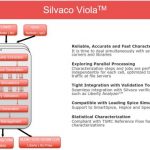
The centerpiece of their library characterization offering is the Viola product which is a complete solution for library characterization. It leverages parallel processing to accelerate the results. It also offers tight links to validation tools. Not only does it work with Silvaco’s SmartSpice, it also works with other leading simulators, such as HSPICE and Spectre. Lastly it is compliant with TSMC’s reference flow for statistical characterization.

Silvaco has thought through the requirements for library characterization for different types of enterprises and projects. Based on the webinar presentation, they are putting together an attractive set of business models, coupled with matched technical elements. To understand the challenges and their complete solution I suggest visiting their website to view the entire webinar.


With Great Power Comes Great Visuality

With Great Power Comes Great Visuality
by Daniel Nenni on 03-29-2019 at 12:00 am

Every system-on-chip (SoC) designer worries about power. Many widely used electronics applications run on batteries, including smartphones, tablets, autonomous vehicles, and many Internet-of-Things (IoT) devices. Even “big iron” products such as network switches and compute servers must be careful when it comes to power consumption. Not every customer can be located next to a hydroelectric dam or a power plant. Even those users willing to pay for vast amounts of electricity may have to comply with “green” laws that cap their draw on the grid.

In response to these requirements, the industry has developed a wide range of techniques to manage power consumption, from clever circuit designs to system-level software control. The most common approach is turning off portions of the SoC not currently active and then turning them back on when required. Instead of being completely powered on and off, the voltage and/or clock speed of a clock domain may be raised or lowered “on the fly” as needed to satisfy critical functionality and meet performance goals.

SoCs may contain dozens of clocks domains with thousands of possible off/on combinations, only some of which are legal. Power controllers that scale the domains up and down are very complex. It is a significant challenge for designers to understand the full scope of power management and for verification engineers to check all legitimate combinations. The consequences of a bug can be severe; a power domain that can’t be turned back on could lock up the chip. Even worse, too many domains powered on at the same time could lead to thermal runaway and chip failure.

So what is the poor SoC engineer to do? I recently talked with Cristian Amitroaie, the CEO of AMIQ EDA, about the power-domain visualization and navigation capabilities in their Design and Verification Tools (DVT) Eclipse Integrated Development Environment (IDE). It seems to me that their approach makes it much easier for design and verification engineers to create, manage, and validate power domains, from IP blocks all the way up to large SoCs. I’d like to review some of the features that struck me.

For a start, DVT Eclipse IDE handles both common formats for specification of power intent, including power domains. Common Power Format (CPF) came from The Silicon Integration Initiative (Si2), while Accellera defined Unified Power Format (UPF). UPF has been standardized as IEEE Std. 1801-2015, which was an attempt to merge the two formats. CPF advocates argue that the IEEE standard is missing some key features, but since AMIQ EDA supports both UPF/IEEE and CPF (version 2.0), SoC teams are free to choose their preferred format.

One critical feature in DVT Eclipse IDE is automatic generation of power supply diagrams from an IEEE Std. 1801 or CPF specification. These diagrams show all the power domains, the connections between them, and the signals from the RTL design that control the domains. Engineers can click on a power domain and jump to the location in the power-intent file specifying the details for the domain. Engineers can also click on a control signal in the diagram and jump to that same signal in the RTL source file. Thus, it is easy to cross-check the design and power-intent files.

This ability is very useful since an IEEE Std. 1801 or CPF file is distinct from the RTL design files. This enables the separation of power intent from implementation, good practice when dealing with any sort of architectural specification. The downside is that it is common for the two descriptions to get out of synchronization as the design evolves. Renamed signals and changes in the design hierarchy can render the power intent file outdated. As Cristian points out, the visualization capabilities of DVT Eclipse IDE make it easy to keep track of changes.

The IDE includes analysis engines “under the hood” that check for many types of problems. Any inconsistencies between the power-intent file and the design are detected and reported visually. DVT Eclipse IDE re-compiles its internal model whenever code changes are made, so it instantly cross-checks any edits to UPF/CPF or RTL files and reports any mismatches. The IDE also detects any syntax or format errors made in any of the design and verification files, including power intent.

In addition to the language and consistency checks, users specifying power domains can benefit from the same features available for all the other languages and formats supported by the IDE. Available features include the power supply network diagrams, source code editors, a hierarchy browser, and schematics of the design. It is easy to navigate among these screens while following a signal or an element in the hierarchy. Color coding is used to visually link common elements across multiple views.

If an engineer makes a mistake, for example typing “create_power_domains” into the UPF editor, the IDE instantly reports this as an error and recommends a correction to the proper “create_power_domain” command. The IDE also makes suggestions; typing in only “create_” pops up a menu showing the possible auto-completions and allowing the user to choose. The IDE can also generate a template for a new command, showing which fields the user must fill in, with both auto-completion options and error reporting available.

Cristian reports that their solution greatly reduces the time it takes to learn a standard and to create a power-intent specification, even for expert users who know the format well. The challenges of SoC power management continue to grow, and it’s hard to imagine designing or verifying a large chip without the support of DVT Eclipse IDE. More information is available, as is a short but impressive video. I encourage you to investigate further, absolutely.

To learn more, visithttps://dvteclipse.com/products/dvt-eclipse-ide.

Also Read

Renaming and Refactoring in HDL Code

I Thought that Lint Was a Solved Problem

Easing Your Way into Portable Stimulus


Spring Forward with AI

Spring Forward with AI
by admin on 03-28-2019 at 5:00 am


The euphoria of NCAA March Madness seems to spill over into the tech world. The epicenter of many tech talks this month spanning from GPU conference, OCP, SNUG to CASPA has evolved around an increased AI endorsement by many companies and its integration into many silicon driven applications. At this year CASPA Spring Symposium, many prominent industry and academic leaders shared their perspectives on the proliferation of AI augmentation into the Internet of Things and the impact of AI of Things (AIoT) on the future of semiconductor industry.

Following is the excerpt of a presentation given by Dr. Steve Woo, Fellow and Distinguished Inventor at Rambus Inc. on ‘AI in the Era of Connectivity’. Since joining Rambus, Steve has worked in various roles leading architecture, technology, and performance analysis efforts as well as in marketing and product planning roles, leading strategy and customer related programs.

Steve was very upbeat about the current transformation we are living in. Driven by the recent advances in neural networks and the rise of powerful computing platforms, AI’s reach and impact on our society has broadened. “In our interconnected world, the needs of data centers, edge computing and mobile devices are continuing to evolve as the role of AI in each vertical segment is evolving as well,” he said. However, the critical challenges remain for enabling higher performance, more power efficient and secure infrastructures supporting AI –all of which offer opportunities for the semiconductor industry.

Digital Data Growth

He added that while the industry demand for performance and capabilities due to the digital data surge is trending up, the primary tools that the industry has relied on for decades, Moore’s Law and Dennard scaling, are slowing or no longer available. A critical challenge will be figuring out how to continue providing more performance and power efficiency in their absence. The infrastructure itself is important as it has incredible values in managing data.

With the amount of growing digital data globally, the memory, link and storage performances have to keep-up in moving data to the processor engine, while both compute and I/O power efficiency must continue to improve as well. The emergence of edge computing has also imposed high performance and low power need for training and inference. He highlighted several steps to mitigate such a demand. This includes at the cloud level: to analyze broad behaviors and pushing the models to the edge and endpoints; at the edge/endpoints to be more selective in communicating processed and higher value data instead of raw data; and having a cloud-processing closer to data (at or near endpoints) –thus, improving the data latency, bandwidth and energy use as well as reducing stress on the underlying network.

AI Needs Memory Bandwidth

The memory bandwidth is a critical resource for AI applications. Inference tasks on older, general purpose hardware such as Haswell, K80 performs well as applications may benefit from the compute and memory optimizations. On the other hand, inferencing on newer silicon such as the Google TPUv1 built for AI processing is largely limited by the memory bandwidth.

There are three well known options to common memory systems for AI applications: On-Chip memories, HBM (High Bandwidth Memories), and GDDR (Graphics Double Data Rate). On-Chip memory offers highest bandwidth and power efficiency as implemented in Microsoft’s BrainWave and Graphcore’s IPU. HBM implementation in products such as AMD Radeon Rx Vega 56, Tesla V100 offers very high bandwidth and density. The additional interposer/substrate and new manufacturing/assembly methods may require additional risk to be dealt with as it is not as well understood as DDR or GDDR cases. The third option, GDDR as found in products such as nVidia GeForce RTX2080Ti delivers good tradeoff between bandwidth, power efficiency, cost, and reliability. The current mainstream refresh for HBM is HBM2 and GDDR is GDDR6, respectively.

Security is paramount

Security around data is also becoming a concern as cyber related attacks are increasingly targeting infrastructures, not just the individual users. Both usage sharing of cloud hardware and the growing system complexity have expanded the surface vulnerability area to exploits. His take is to not compromise security in lieu of a good performance gain. “Security must become a first‐class design goal, we cannot treat security as an afterthought and attempt to retrofit it into silicon and systems,” he stated.

Recent exploits like Spectre, Meltdown, and Foreshadow have shown that security can be compromised through unexpected interactions between features in the processor. Processors are becoming more complex, meaning the number of interactions is growing exponentially. This has led the industry to conclude that new approaches are needed for providing secure computing. One such approach that Steve discussed is siloed execution. In this scenario, physically distinct CPUs are utilized that process secure operations and secret data on a security CPU, while non-secure applications and data can be processed on a general-purpose CPU. The general-purpose CPU can be as performant and feature-rich as necessary, while the security CPU can be simple and optimized for security. Segregating processing and data in this manner also allows secret data to remain secret even if the general-purpose CPU is hacked.

Steve elaborated more on Rambus security solution called CryptoManager Root of Trust, which is comprised of customized RISC-V CPU and a Crypto Accelerators and secure memory components. It provides secure boot, remote attestation, authentication with various encryption modes (such as AES, SHA) and runtime integrity. The following diagram illustrates how it may be augmented into an AI system capable of operating in cloud environments by decrypting multiple user training sets and models using different keys, and running them on cloud AI hardware.

To recap, AI is driving a renaissance in computer architecture and memory systems. The conflict between performance and security is more pronounced as data and insights are increasingly more valuable. Along this line, design teams need to ensure addressing the security aspects on top of design complexity as it only takes one vulnerability for hacker to compromise the entire system and data security.

For more info on Rambus, please check HERE


Managing Formal Complexity Even into AI

Managing Formal Complexity Even into AI
by Bernard Murphy on 03-27-2019 at 7:00 am

The Synopsys Formal group have a reputation for putting on comprehensive tutorials/workshops at DVCon and this year again they did not disappoint. The theme for the Thursday workshop was tackling complexity in control and datapath designs using formal. Ravindra Aneja, who I know from Atrenta days, kicked off the session with their main objective: to overcome common concerns raised by folks interested in formal but concerned about the extent to which it can contribute. These should sound familiar: on what types of design can I use formal, how well does it scale to large functions and what do I really save by using formal?

Ashish Darbari, CEO of Axiomise next presented on formal for SoC designs. I don’t think I can do justice to his full presentation, so I’ll just mention a few points he emphasized for scalability. First, and most obviously, apply formal to smaller functions (such as complex state machines) that are so tangled they are really hard to verify comprehensively using dynamic verification. For larger functions, he suggests using a method he calls proof-engineering; this is simply breaking down a larger problem into smaller pieces which you can prove individually and then assemble into fuller, more complete proofs on the larger system. That shouldn’t be too scary – it’s engineering 101 after all. He talks about common methods in formal to handle these, including assume-guarantee and case-splitting. Don’t worry about the jargon; the underlying concepts in these techniques are not at all complicated.

Nitin Mhaske (another Atrenta alum) next talked about using formal to verify control logic. generally considered to be the sweet spot for formal. Widely cited examples in this space include complex state controllers; Nitin use a PCIe/USB LTSSM and a 10G/40G Ethernet state controller. I would add cache coherency controllers as another good example. What all of these have in common is many states and multiple paths to those states, complex state transition conditions and difficulty in ensuring that all possibilities have been considered in verification. Nitin detailed techniques to attack verification of these systems, also how to look deeper in a design using bug-hunting to check behavior beyond what you can intuitively see.

The final section attracted me especially because the speaker (Per Bjesse of Synopsys) talked about formal verification of datapaths, a topic typically considered a no-no for formal. Synopsys have been quietly advancing their HECTOR™ technology (now under the hood in their DPV app) for several years now and seem to have some serious customer validation. These include proofs from 32-bit to 128-bit FPUs across all the standard opcodes from ADD to MULT, DIV and SQRT, many completing in minutes, others in no more than a few hours and the most complex in around 6 hours.

They have also discovered that this analysis is particularly promising for proofs in systolic arrays of multiply-accumulate (MAC) functions. Does that sound familiar? It should; these are the basis of neural net (NN) architectures. Of course proofs at this level are not going to prove that an image is correctly recognized, but they will prove that the foundation logic matches the intended implementation. This is not as trivial in many cases as it may sound; for example, it has become very common to have varying and non-standard word-widths between planes in inference NNs at the edge. I can imagine this foundational level of verification could prove quite important in the overall verification plan.

What’s under the hood? I was told that the number of proof engines is often smaller than for control proving, and includes the familiar BDD, SAT and SMT methods, though more tuned to datapath proofs. Since a good deal is automated, effort in using this technology can actually be simpler than for general formal verification; examples mentioned were integer multiply (with a result < 20 bits), AES single round and floating-point half-precision. Also, the datapath-proving algorithms work with both C and RTL, a significant convenience when verifying algorithms developed in C/C++ and obviously allowing for much faster proofs at this higher level of abstraction. My take-away? If you’re still on the fence about formal, scalability is manageable, proving in control logic already has well-established value and proving in datapath logic is now looking more practical. As for value in the overall verification task, many companies are already doing this as an adjunct to dynamic verification. They have reported that it saves them time, because their formal group can start finding bugs while the dynamic folks are still building testbenches. It adds confidence because those functions that have been proven formally are known to be solid. And it mostly replaces simulation for those functions assigned to formal proving. I say mostly because I have seen cautious verification managers still use interface assertions from formal proofs in dynamic testing. But they’re not repeating the formal testing, they just want added confidence (after all, the people who created the formal properties can make mistakes too).

You can learn more about the full range of Synopsys formal capabilities HERE.


Hierarchical RTL Based ATPG for an ARM A75 Based SOC

Hierarchical RTL Based ATPG for an ARM A75 Based SOC
by Tom Simon on 03-27-2019 at 5:00 am

Two central concepts have led to the growth of our ability to manage and implement larger and larger designs: hierarchy and higher levels of abstraction. Without these two approaches the enormous designs we are seeing in SOCs would not be possible. Hierarchy in particular allows the reuse of component blocks, such as CPU cores. This has been a major enabling element to SOC designs. Due to the very real clock rate ceiling for practical CPU implementation, the move to multiple parallel processors has been essential to increasing performance without running into power and bandwidth issues.

Back in the late 1990’s physical chip design was hierarchical, and it was Mentor that lead a revolution in leveraging hierarchy for DRC. Now, Mentor is a leader in the move to make DFT and ATPG hierarchical, taking special advantage of repeated blocks. They have moved test insertion and test operations themselves to the block level, unlocking many efficiencies and reducing overall complexity. Mentor’s Tessent Hierarchical ATPG Flow at the RTL level offers many advantages.

Mentor and ARM have published a reference flow showing how DFT and ATPG can be implemented at RTL in an SOC containing multiple Cortex-A75s. Fully one third of the reference flow introduction is documentation of the steps used in the flow. This provides useful technical information useful for implementation. The first part of the document discusses the approach and advantages of the flow.

For the purposes of the reference flow, which uses 4 instances of the A75, they implemented two levels of DFT: the wrapped A75 core and top-level logic. Once the A75 core is wrapped it can be placed multiple times in the SOC. The finished chip contains MBIST and 1149.1 boundary scan logic. Also included are on-chip clock controllers (OCC), Tessent TestKompress controllers (EDT) and the test access mechanism (TAP).

The flow starts with MBIST insertion in the A75 block, followed by EDT and OCC insertion, all at RTL. After this, block synthesis is performed as usual. Next is scan insertion and retargetable ATPG for the block. Within the A75 the Tessent MBIST can use the shared memory bus. Once the A75 is done with test, the reference flow moves on to the top-level logic.

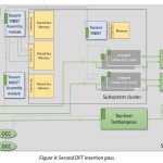
For the top level, boundary scan and MBIST are added first. A JTAG compatible TAP controller, Tessent boundary scan logic, an IJTAG-based Tesesnt MBIST assembly module for shared bus memories in the chip top level, and also regular Tessent MBIST for individual memories are added next. A second pass adds TestKompress logic and OCCs. The design also gets TAMs that can support multiple ATPG test modes. Each of the already wrapped A75s are included during the second pass.

So, what are the results? At the core level with 6,365 patterns for Stuck-at faults, they reach a coverage of 99.21%. For Transition faults, with 17,791 patterns, the coverage is 98.28%. In each case these numbers are just shy of the ‘ideal’ total for extest and intest coverage. Here are the top level ATPG results.

As I mentioned earlier, this is a detailed step by step description of the flow and includes actual annotated command descriptions for the process. This documentation shows the value of the partnership between ARM and Mentor and provides useful insight into the actual flow and its results. For users wishing to take this to the next level, the full reference flow package available from Mentor includes everything needed to implement this flow, including scripts, interfaces and documentation. To get started I’d suggest reading the overview from the Mentor website.


Menta eFPGA Conquer Eu Processor and 5G in China

Menta eFPGA Conquer Eu Processor and 5G in China
by Eric Esteve on 03-27-2019 at 12:00 am

During 2018, Menta looked quiet if you consider communication as the main indicator of activity. In fact, the eFPGA vendor was hyper-active in developing future business and reports two main design-win. The first is with the European Processor Initiative (EPI) and Menta has announced in December 2018 that it has been selected as the sole provider of embedded FPGA IP for this European project.

This is significant for Menta in driving programmability in a large share of new high-performance computing and automotive applications. Members of the consortium include Atos, BMW, CEA, Infineon and ST Microelectronics.

The second design win officially announced by Menta a few days ago is with a Telecom company in China, as “eFPGA IP from Menta Selected by Beijing Chongxin Communication Company to Enable Programmability in 4G/5G Wireless Baseband SoC”. It’s important to show that eFPGA IP is now considered as mature enough to be integrated into a wireless SoC addressing the very competitive 4G/5G market.

In other words, all design win doesn’t weight the same. Winning a prototype project developed by a research team working in a prestigious university is great, but integrating an eFPGA IP in a SoC expected to go in production is even better and demonstrate that embedded FPGA is moving from lab to industry!

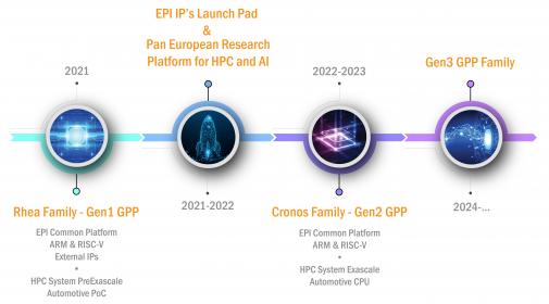
Nevertheless, being selected to serve the EPI is a wise investment to serve the automotive industry in the future. If we must select one industry segment where Europe is competitive, automotive certainly comes in first. The main goals of the EPI project are:

  • European independence in High Performance Computing Processor Technologies.
  • EU Exascale machine based on EU processor by 2023.
  • Based on solid, long-term economic model, Go beyond the HPC market.
  • Address the needs of European Industry (Car manufacturing market).

I love the last two goals, showing the willingness to keep pace with long-term economic model and to address the needs of the automotive industry. It looks obvious today, but such big project may have failed in the past to be economy-compatible. And, because car manufacturing is a competitive market, we know that it can turn into an economic war between USA, China and Europe. In modern wars, you need to consider semiconductor as ammunitions!

We can expect the automotive CPU issued from EPI to integrate eFPGA IP, as it’s the best way to provide efficient flexibility to a SoC. Especially when this SoC will be integrated to a car and must be functional for at least a decade, but also be able to be updated when needed.

If we consider the total European automotive industry, the production volume is in the 20 million vehicles range. To obtain the SoC production volume TAM, you have to multiply the number of cars by the number of CPU per car… It may become a huge number, approaching the billion SoC per year (just look at the next picture). Yes, eFPGA IP design win in EPI can be a very wise investment!


The other (officially announced) design win, the baseband SoC from Beijing Chongxin Communication Company is expected to support both the existing 4G LTE infrastructure while also offering the programmability required to address the emerging 5G NR wireless specification. And Mr Tao Hu, VP of Engineering of Beijing Chongxin Communication Company, seems to be completely convinced by the benefits of integrating eFPGA IP.

“We are pleased to select Menta’s eFPGA IP for our 5G NR SoC. The eFPGA IP surpassed all other available options on the market in terms of flexibility, technology portability and customer support,” said Tao Hu, VP of Engineering of Beijing Chongxin Communication Company. “Menta’s IP supports of the specifications of our next-generation wireless communication products, including re-configurable and software-defined features. The portability of their IP to all process technologies makes them an ideal long-term technology partner.”


As a conclusion, I will share again that I wrote in 2017 in Semiwiki: “As far as I am concerned, I really think that the semiconductor industry will adopt eFPGA when adding flexibility to a SoC is needed. The multiple benefits in term of solution cost and power consumption should be the drivers, and Menta is well positioned to get a good share of this new IP market.”

These two design wins represent a fact-based confirmation of this prediction, isn’t it?

From Eric Esteve from IPnest


Verification 3.0 Holds it First Innovation Summit

Verification 3.0 Holds it First Innovation Summit
by Randy Smith on 03-26-2019 at 5:00 am

Last week I attended the first Verification 3.0 Innovation Summit held at Levi’s Stadium in Santa Clara along with about 90 other interested engineers and former engineers (meaning marketing and sales people, like me). There was a great vibe and feel to the event as it exuded an energy level that I have not felt at an EDA event in years. The attendees included longtime EDA veterans as well as a few newcomers. Perhaps more important, the list of participating companies was quite long including speakers from Avery, Breker, Metrics, TV&S, Imperas, OneSpin, Vayavya, Agnisys, Concept, Methodics. Vtool, and Verifyter. Blue Pearl, Willamette HDL, and XtremeEDA were also supporting the event. Quite a collection of verification experts. All these companies gave presentations, spoke to attendees in a tabletop gathering at the end of the event (with great food!), or did both.

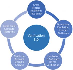
EDA industry luminary, Jim Hogan, who has been a driving force behind the Verification 3.0 effort, kicked off the event. Jim is involved in several of the companies supporting this effort as a consultant, investor, and board member. Unfortunately, due to traffic, I missed Jim’s remarks, but we did get a chance to talk at the reception later in the evening where Jim told me, “There are some major themes that Joe outlined in his talk. It’s time to take a new approach to verification, that’s why we called it verification v3.0. We outlined this in an article last year.” Herding so many start-ups is quite a challenge, but Jim is off to a terrific start.

Next up was Joe Costello, former Cadence CEO and the “Tony Robbins of EDA”. I worked at Cadence during Joe’s tenure and his infectious smile, positive attitude, and fervent enthusiasm were clearly all still in effect. Joe laid out a clear case for the likely path of verification solutions over the next five years. He discussed the macroeconomic factors and the design trends that are driving a new approach to verification solutions and then suggested a target opportunity for the participating companies.

The first macroeconomic factor mentioned by Joe is the move to cloud computing. The cloud computing market is already in the same order of magnitude as the entire semiconductor market, measured in the hundreds of billions of dollars per year. Yet, most EDA companies have been slow to make use of these services. Cloud-based EDA solutions would stop semiconductor designers from also needing to be experts at running their own massive compute farms. This also goes hand-in-hand with the second macroeconomic factor, SaaS (software as a service). Deploying EDA tools as a service is far simpler to do in a cloud environment where both the use of the hardware AND software would be measured. This allows users to only pay for the tool usage they use, rather than pay for (and try to predict) their maximum needed capacity of licenses.

So, you might be thinking that these are just infrastructure issues, it is not the next algorithm or paradigm to solve verification issues. What I can tell you is the biggest hurdle of semiconductor design today is the COST of verification. That cost is in licenses and hardware – but it is especially important in headcount. Having spent some time the last few years helping firms on their recruiting challenges, I know for certain that there are not enough verification engineers available to meet the semiconductor industry’s current needs. So, improving efficiency in verification is critical to improving the results of verification as well as reducing its costs.

Improving the efficiency of verification also can mean building more platforms which are specific to certain types of designs. Joe specifically mentioned the fledgling market for design specific processors. Domain specific processors are coming about due to the end of Moore’s Law and Dennard scaling, as well as the concerns about efficiently scaling solutions. Building processors for specific applications is an approach to improve the efficiency and results of designs build for specific problems. Joe specifically mentioned ‘RISC-V’ as an example of open processors enabling this approach. Now doubt, ARM could also go down this path to some extent as well.

Which leads us to this: If you are going to have domain specific architectures, then can’t you develop specific verification environments to aid in the design and verification of those designs? For example, why not build an environment around a specific processor (that also supports extensions) including the IP and verification best practices specific to that application – an environment supporting ISO 26262 for functional safety? An environment knowledgeable of video/audio codec standards? The list is long. Beyond the changes this can drive in the verification industry, the opportunities in semiconductor IP are enormous.

This event was well worth attending, and if you are interested in verification, it would be well worth your time to attend the next Verification 3.0 event whenever that might next happen. You can check out the website at https://verification30.com/. I heard slides might be online next week.


Self-Certification Insufficient?

Self-Certification Insufficient?
by Roger C. Lanctot on 03-26-2019 at 12:00 am

The crash of Ethiopia Air Flight 961 may have a negative impact on the development of autonomous vehicle technology. The Federal Aviation Administration (FAA) is now forced to reconsider the “self-certification” process used for the Boeing 737 Max 8 airplane involved.

Self-driving car developers have been seeking the same self-certification for their own systems. The FAA’s failure suggests that may not be good enough. The U.S. Department of Transportation’s National Highway Traffic Safety Administration is taking public comments regarding a regulatory framework for autonomous vehicles, which are already cruising U.S. highways. The challenge for air and land travel governed by software is the same: Understanding and regulating the algorithms and code inside black boxes.

Feds move to consider cars with no steering wheels, brakes – Automotive News

Regulating surface transportation is complicated by the role of local regulators in the U.S. – the 50 states. It is complicated by the fact that many of these states view automated driving technology as the killer app capable of easing congestion, reducing vehicle emissions and enhancing mobility for disadvantaged or disabled populations.

But the killer app might become itself a killer. With each new fatality attributed to an autonomous vehicle, come the investigations to determine what sort of algorithmic failure led to the crash. Thus far, from Florida to Arizona, the source of the software shortcoming seems to have been successfully located – but that may not always be the case.

In the case of Ethiopia Air 961 the story appears to be even worse as multiple reports suggest that a software update was either in the works – to correct the failure experienced by Lion Air Flight 610 – or ready to be implemented, but failed to deploy in time. Another layer to the story derives from the self-certification where, according to reports in the Washington Post, Boeing employees were more or less deputized to act as FAA representatives as part of the process.
Further still, reports have emerged that pilots and airline representatives being shown the new system in the Boeing 737 Max 8 identified multiple areas requiring further training and preparation:

For cars it is not a case of training drivers. It is a case of training machines to drive. We go from the forensic “black box” of the airline industry to the emerging A.I. black box of the self-driving car industry. The question is whether we are inclined to put our “faith” in A.I. from self-driving car developers or with regulators. We already know the limitations of the regulators.

Conferring our faith to the A.I. black box in the self-driving car reminded me of the A.I. challenges currently facing the health care industry. In the words of one interviewee, Dr. Eric Topol, cardiologist and the founder and director of the Scripps Research Translational Institute, quoted in the New York Times last week:

“There’s no shortage of deep liabilities for A.I. in health care. The liabilities include breaches of privacy and security, hacking, the lack of explainability of most A.I. algorithms, the potential to worsen inequities, the embedded bias and ethical quandaries.”

Self-certification in the airline industry – necessitated no doubt by expenses and staffing limitations at the FAA – will now come under renewed scrutiny. Will self-certification be good enough for self-driving cars?

The incompetence and failure at Boeing and the FAA raise unavoidable questions regarding the regulation of transportation. The latest fatal Tesla crash (with a semi-trailer), just a few weeks ago, and these two 737 Max 8 crashes are testing the tolerance of transportation users.

U.S. safety agencies to investigate fatal Tesla crash in Florida – CNBC

The debate calls to mind a presentation I gave last week at a security conference put on by the Metropolitan Police in the U.K. I concluded by noting the likelihood that regulators will require the ability to remotely control autonomous vehicles. In other words, regulators will not allow autonomous vehicles unless there is a provision to control them remotely.

Not surprisingly, some of the law enforcement members in the audience wanted to discuss the topic in further detail. The story of vehicle remote control is both old and new.

General Motors and Hyundai Motor America offer remote vehicle slow-down functions as part of the stolen vehicle tracking and recovery solution in their telematics offerings for passenger vehicles. Brazil attempted to mandate vehicle immobilizer technology several years ago, but abandoned the effort over privacy and security concerns. Finland’s regulatory authority requires a driver for a certified autonomous vehicle, but the driver need not be IN the vehicle.

Remote control is the main differentiator between airline and surface transportation, which is far more deadly than flying. For now, the airline industry and its regulatory authorities have determined that the risks of remote control for airplanes are greater than the rewards. For cars, it is increasingly looking like remote control will be essential.

Even with remote control, though, the challenge of certification and regulation remains. In the U.S., states are opting for less regulation, not more. An audience at the Future Networked Car Symposium at the Geneva Motor Show voted by a show of hands slightly in favor of more regulation – perhaps reflecting the presence of executives from multiple European regulatory authorities.

Ten years from now we will somehow arrive at the nirvana of autonomous vehicle technology where we are saving lives and reducing congestion, and emissions, and parking garages are eliminated completely. There are going to be bumps along the way. Fasten your seat belt.

Also read: Surviving in the Age of Digitalization