The scope of current system designs continues to present challenges to verification and implementation engineering teams. The algorithmic complexity of image/voice processing applications needs a high-level language description for efficient representation. The development and testing of embedded firmware routines (commonly written in ‘C’) are driving the trend toward SW/HW “virtual prototyping” verification strategies. And, to be sure, the time-to-market (TTM) pressures are extreme – despite the increased scope and diversity, there is little relief in design schedules. To improve design productivity and verification throughput, hardware models must be represented at higher levels of abstraction, while also providing a well-defined synthesis flow to implementation.
The SystemC hardware description language was originally conceived to help address these design modeling and verification pressures. Yet, SystemC adoption has been slow. The overall language semantics were well-defined, but the modeling guidelines for implementation synthesis were unclear. And, significantly, the influence and support of a “standards” organization for SystemC modeling was lacking. At the recent DVCon (Design and Verification Conference) in San Jose, a workshop session focused on SystemC provided a very positive update on the issues above – indeed, I would anticipate an acceleration in adoption by system designers.
First, a standards update…
Mike Meredith from Cadence Design Systems described the initiatives within Accellera to define and document SystemC usage guidelines. The list of active working groups is impressive:
- SystemC Language
- SystemC Synthesis
- SystemC Verification
- SystemC Datatypes
- SystemC Analog/Mixed-Signal
- SystemC Configuration, Control, and Inspection
The other workshop participants added to Mike’s overview, with encouraging comments.
“The Accellera initiatives are expanding beyond the base language definition, with use case examples covering ‘what to model’ and ‘how to model’.”
“The Accellera activities have focused on clarifying the relationship and distinctions between SystemC (v2.3.3) and C++(v11/v14).”
“A draft of the SystemC library integration with the Universal Verification Methodology(UVM)has been prepared – for example, how to adapt a System Verilog constrained random testbench to exercise SystemC models.”
“The unique nature of automotive system designs requires both the productivity of SystemC and AMS simulation integration. The Accellera working group has been updating the SystemC/AMS user guide and regression test suite, describing in detail the synchronization activity between the(continuous domain)analog and(discrete event)digital models.”
“The high-level synthesis semantics of SystemC assertions is a focus area, in support of assertion-based verification(ABV)environments.”
Mike expanded upon the last comment above, to describe the main emphasis of the Accellera SystemC synthesis working group, namely the development of a SystemC modeling standard for high-level synthesis (HLS).
HLS for SystemC involves a sequence of algorithms to realize an implementation-based model:
- elaboration
- input synthesis directives and constraints
- characterization of the hardware resources for all operations
- scheduling operations to clocks
- generation of the RTL model
To enable SystemC synthesis, additional “hardware-centric” features were needed – e.g., modules, ports, signal, processes, bit-accurate datatypes, communication channels, and clocks. SystemC synthesis directives are also unique, offering (optional) user guidance on:
- program loop interpretation (e.g., “UNROLL_LOOP”)
- resource allocation (i.e., binding operations to resources)
- cycle scheduling (e.g., pipelining evaluations, latency)
- allocation and mapping to registers
- reset behavior
- creation of finite-state machine states and transitions
- definition of data channels (e.g., point-to-point interfaces, FIFO’s, etc.)
- pin-level protocols for data communication (with SystemC function calls through an event on a “SC_port”)
Even with cycle-accurate definitions for protocols and controls, the base algorithm models are still abstract – SystemC for HLS maintains its design and verification productivity.
Mike went into detail on the most significant updates to SystemC modeling for HLS, specifically how the model structure is defined, and how (implicit) clocking is incorporated. His illustrations used the concept of a SystemC “thread” (process).
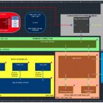
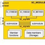
The figure below illustrates the SystemC module structure for HLS (from Mike’s DVCon presentation). The structure contains elements familiar to RTL designers – e.g., ports for hierarchical connectivity and signal communication.
The definition of a concurrent sequential process is fundamental to RTL modeling, and is reflected in SystemC (for HLS) as an “SC_METHOD” or “SC_THREAD”. The figures below illustrate the features of these processes, and a brief coding example, applicable to both verification and synthesis.
The SC_THREAD and SC_CTHREAD include both a reset preamble and a “wait()” function to represent clocked evaluation. (Briefly, the SC_THREAD process is sensitive to any event, whereas the SC_CTHREAD is suspended by a clock signal – the SC_CTHREAD process is used to define a FSM in the output RTL model.)
The SC_METHOD would not include any wait suspension execution control. Note that the verification flow is directed to execute the reset code by “registering” the thread/process, as opposed to the semantics of a constructor function. (A constructor would only be evaluated once, whereas a model reset may be re-executed as part of verification.)
Mike also described the SystemC standards activity for synthesis of variable datatypes, using 2’s complement evaluation – see the figure below.
“Not all users will need the full datatype width of standard.”, Mike highlighted. “For more efficient hardware implementation through synthesis, other bit width datatypes are available in the Accellera SystemC library. For non-integer numeric datatypes, user-defined behavior for the saturation and rounding of a calculation is provided.”
I left the DVCon SystemC workshop very enthused about the progress of the Accellera working groups, and the standards activity to define SystemC semantics for HLS. Admittedly, only two EDA vendors are currently providing SystemC HLS support. Regardless, I expect the interest in SystemC modeling to grow and the adoption rate to increase.
Design and verification engineers interested in learning more about SystemC (and ideally, participating in the working groups) are encouraged to go to the Accellera web site (link).
For more information on the Cadence Stratus HLS offering, please go to this link.
-chipguy