

The semiconductor foundry business has gone through a dynamic transformation over the last 30 years. In the beginning the foundries were several process nodes behind the IDMs with little hope of catching up. Today the foundries are leading the process development race at 10nm – 7nm, and will continue to do so, absolutely.
If you look at the foundry landscape, TSMC has the advantage because they are TSMC, the trusted foundry partner with the most mature and complete ecosystem bar none. TSMC is also a process technology leader and fierce competitor.
The market for Samsung Foundry as I see it is three-fold:
- They are not TSMC. Capacity is not an issue with Samsung and it is always good to have foundry options. TSMC and Samsung are the only two leading edge foundries left so this is a much bigger point than most imagine.
- Technology. Leading edge fabless companies look for the best technology that will also meet their time to market requirements. Samsung was ahead of TSMC at 14nm and they did quite well at that node. At 10nm and 7nm Samsung was a bit behind TSMC but Samsung 7nm had EUV before TSMC so some fabless companies are now leading with Samsung.
- Pricing. Samsung has the best wafer pricing the industry has ever seen. Being the largest memory manufacturer does have its advantages and wafer pricing is one of them.To catch up with the latest on foundry process technology I talked to Scotten Jones, internationally recognized semiconductor expert and founder of IC Knowledge, a technology consulting company that models the economics of semiconductors. Scott has been writing for SemiWiki since 2014, his blogs are on the IC Knowledge landing page. Here are Scott’s latest thoughts on TSMC versus Samsung at 7nm:
- Contacted Poly Pitch (CPP) – both TSMC and Samsung claim a CPP of 54nm for 7nm but for both of them I believe their actual CPP for cells is 57nm.
- Metal 2 pitch (M2P) – Samsung is 36nm and TSMC is 40nm.
- Tracks – Samsung minimum cell track height is 6.75 and TSMC is 6.0.
- Diffusion break – TSMC optical process (7FF) is double diffusion break (DDB) and they are reported to be going to single diffusion break (SDB) for their EUV process (7FFP). Samsung 7nm has a 1[SUP]st[/SUP] generation process (I believe this is 7LPE) and it is DDB, they also have a second generation process (I believe this is 7LPP) that is also DDB. At VLSIT this year they talked about a 3[SUP]rd[/SUP] generation process with SDB. It is hard to know what this really is, at 10nm their second generation process was actually their 8nm process so this could be their 5nm process or it could really be a third generation 7nm process.
- Transistor density – the minimum cell logic density for TSMC 7FF is slightly better than Samsung 7LPE or 7LPP. TSMC EUV 7FFP is slightly better than Samsung “3[SUP]rd[/SUP] generation” 7nm.
- SRAM cell size – I think the SRAM cell size is the same for all three Samsung generations (I have a number for the 3[SUP]rd[/SUP] generation process) and both TSMC generations (I have a number for 7FF) but I am not positive. Samsung has a slightly smaller SRAM cell.
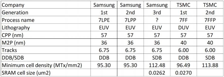
According to Scott, overall, the two processes are similar in density with TSMC leading in the ramp-up and likely yield and I agree, absolutely.


TSMC CoWoS versus Intel EMIB Semiconductor Packaging