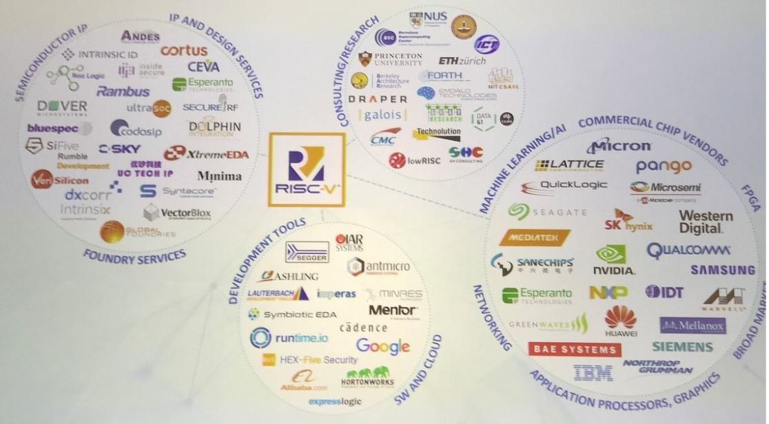
Bronco Webinar 800x100 1

The 7 Most Dangerous Digital Technology Trends

The 7 Most Dangerous Digital Technology Trends
by Matthew Rosenquist on 01-01-2019 at 6:00 am

The 7 Most Dangerous Digital Technology Trends

As our world embraces a digital transformation, innovative technologies bring greater opportunities, cost efficiencies, abilities to scale globally, and entirely new service capabilities to enrich the lives of people globally. But there is a catch. For every opportunity, there is a risk. The more dependent and entrenched we become with technology the more it can be leveraged against our interests.  With greater scale and autonomy, we introduce new risks to family health, personal privacy, economic livelihood, political independence, and even the safety of people throughout the world.

As a cybersecurity strategist, part of my role is to understand how emerging technology will be used or misused in the future to the detriment of society.  The great benefits of the ongoing technology revolution are far easier to imagine than the potential hazards. The predictive exercise requires looking ahead to see where the lines of future attackers and technology-innovation intersect. To that end, here is my 2019 list of the most dangerous technology trends we will face in the coming months and years.

Top 7 Most Dangerous Digital Technology Trends

1.      AI Ethics and Accountability

Artificial Intelligence (AI) is a powerful tool that will transform digital technology due to its ability to process data in new ways and at incredible speeds. This results in higher efficiencies, greater scale, and new opportunities as information is derived from vast unstructured data lakes. But like any tool, it can be used for good or wielded in malicious ways. The greater the power, the more significant the impact.

Weak ethics may not seem worthy of being on the list, but when applied to the massive adoption, empowerment, and diversity of use-cases of AI, the results could be catastrophic. AI will be everywhere. Systems designed or employed without sufficient ethical standards can do tremendous harm, intentionally or unintentionally, at an individual and global scale.

Take for example how an entire community or nation could be manipulated by AI systems generating fake news to coerce action, shift attitudes, or foster specific beliefs. We have seen such tactics happen on a limited scale to uplift reputations of shady businesses to sell products, undermine governments, and lure victims into financial scams. By manipulating social media, advertising, and the news, it is possible to influence voters in foreign elections, and artificially drive the popularity of social initiatives, personalities, and smear campaigns. Now imagine highly capable systems to conduct such activities at a massive scale, personalized to individuals, relentless in the pursuit of its goal, that quickly improves itself over time with no consideration of the harm it is causing. AI can not only inundate people with messages, marketing, and propaganda, it can also tailor it to the individuals based upon specific user’s profile data, for maximum effect.

AI systems can also contribute and inadvertently promote inequality and inequity. We are still in the early stages where poor designs are commonplace for many AI deployments. It is not intentional, but a lack of ethical checks and balances result in unintended consequences. Credit systems that inadvertently favored certain races, people living in affluent areas, or those who support specific government policies have already been discovered. Can you imagine not getting a home or education loan because you happen to live on the wrong side of an imaginary boundary, due to your purchasing choices, or your ethnicity? What about being in a video conference but the intelligent system does not acknowledge you as a participant because it was not trained to recognize people with your skin color? Problems like these are already emerging.

AI systems are great at recognizing optimal paths, patterns, and objects by assigning weighted values. Without ethical standards as part of the design and testing, AI systems can become rife with biases that unfairly undermine the value of certain people, cultures, opinions, and rights. This problem propagates, potentially across the spectrum of systems and services leveraging AI, and to impact people through the layers of digital services that play a role in their life, thereby limiting what opportunities they can access.

A more obvious area where AI will greatly contribute to the undermining of trust and insecurity is via synthetic digital impersonations, like ‘deepfakes’ and other forms of forgery. These include videos, voices, and even writing styles that AI systems can mimic, making audiences believe they are interacting or conversing with someone else. We have seen a number of these emerge with political leaders convincingly saying things they never did and with celebrities’ likenesses being superimposed in sexually graphic videos. Some are humorous, others are intended to damage credibility and reputations. All are potentially damaging if allowed to be created and used without ethical and legal boundaries.

Criminals are interested in using such technology for fraud. If cybercriminals can leverage this technology at scale, in real-time, and unimpeded, they will spawn a new market for the victimization of people and businesses. This opens the door to create forged identities that are eerily convincing and will greatly contribute to the undermining of modern security controls.

Scams are often spread with emails, texts, phone calls, and web advertising but have a limited rate of success. To compensate, criminals flood potential victims with large numbers of solicitations anticipating only a small amount will be successful. When someone who is trusted can be impersonated, the rate of success climbs significantly. Current Business Email Compromise (BEC), which usually impersonates a senior executive towards a subordinate, is growing and the FBI estimates it has caused over $26 billion in losses to American companies in the past 3 years. This is usually done via email, but recently attackers have begun to use AI technology to mimic voices in their attempts to commit fraud. The next logical step is to weave in video impersonations where possible for even greater effect.

If you thought phishing and robocalls were bad, standby. This will be an order of magnitude worse. Victims may receive a call, video-chat, email, or text from someone they know, like a coworker, boss, customer, family member or friend. After a short chat, they ask for something: open a file, click on a link, watch a funny video, provide access to an account, fund a contract, etc. That is all it will take for criminals to fleece even security-savvy targets. Anybody could fall victim! It will be a transformational moment in the undermining of trust across the digital ecosystem and cybersecurity when anyone can use their smartphone to impersonate someone else in a real-time video conversation.

Creating highly complex AI tools that will deeply impact the lives of people is a serious undertaking. It must be done with ethical guardrails that align with laws, accepted practices, and social norms. Otherwise, we risk opening the doors to unfair practices and victimization. In our rush for innovation and deployment, it is easy to overlook or deprioritize a focus on ethics. The first generations of AI systems were rife with such bias as the designers focused on narrow business goals and not ramifications of outliers or the unintended consequences of training data that did not represent the cross-section of users. Our general inability to see future issues will amplify the problems.

AI is a powerful enabler and will amplify many of the remaining 6 most dangerous technology trends.

2.      Insecure Autonomous Systems

As digital technology increases in capabilities, we are tantalizingly close to deploying widespread autonomous systems. Everyone marvels at the thought of owning a self-driving automobile or having a pet robot dog that can guard the house and still play with the kids. In fact, such automation goes far beyond consumer products. They can revolutionize the transportation and logistics industry with self-operating trucks, trains, planes, and ships. All facets of critical infrastructure, like electricity and water, could be optimized for efficiency, service delivery, and reduced costs. Industrial and manufacturing crave intelligent automation to reduce expenses, improve quality consistency, and increase production rates. The defense industry has long sought autonomous systems to sail the seas, dominate the air, and be the warriors on the ground.

The risks of all these powerful independently-operating systems are that if they are compromised, they can be manipulated, destroyed, held hostage, or redirected to cause great harm to economies and people. Worst-case scenarios are where such systems are hijacked and turned against their owners, allies, and innocent citizens. Having a terrorist take control of fleets of vehicles to cause massive fatalities in spectacular fashion, to turn the regional power or water systems off by criminals demanding a ransom, or manipulating industrial sites with caustic chemicals or potentially dangerous equipment could cause a hazard to nearby communities or an ecological disaster.

Autonomy is great when it works as intended. However, when manipulated maliciously it can cause unimaginable harm, disruption, and loss.

3.      Use of Connected Technology to the Detriment of Others

One of the greatest aspects of digital technology is how it has increasingly connected the world. The Internet is a perfect example. We are now more accessible to each other, information, and services than ever before. Data is the backbone of the digital revolution.

However, connectivity is a two-way path. It also allows for unwanted parties to connect, harass, manipulate, and watch people. The impacts and potential scale are only now being understood. With billions of cameras being installed around the world, cell-phones being perfect surveillance devices, and systems recording every keystroke, purchase, and movement people make, the risks of harm are compounded.

Social media is a great example of how growth and connectivity have transformed daily life but have also been used to victimize people in amazing ways. Bullying, harassment, stalking, and subjugation are commonplace. Searching for information on others has never been easier and rarely do unflattering details ever get forgotten on the Internet.

The world of technology is turning into a privacy nightmare. Almost every device, application, and digital service collects data about its users. So much so, companies cannot currently make sense of most of the unstructured data they amass and typically just store what they gather in massive ‘data-lakes’ for future analysis.  Current estimates are that 90% of all data being collected cannot be used in its current unstructured form. This data is rarely deleted and is instead stored for future analysis and data mining.  With the advance of AI systems, valuable intelligence can be readily extracted and correlated for use in profiling, marketing, and various forms of manipulation and gain.

All modern connected systems can be manipulated, corrupted, disrupted, and harvested for their data regardless if they are consumer, commercial, or industrial grade. If the technology is a device, component, or digital service, hackers have proven to rise to the challenge and find ways to compromise, misuse, or impact the availability of connected systems.

These very same systems can facilitate improved terror attacks and become direct weapons of warfare as we have seen with drones. Terror groups and violent extremists are looking to leverage such technology in pursuit of their goals. In many cases, they take technology and repurpose it. As a result, asymmetric warfare increases across the globe, as connected technology is an economical force-multiplier.

The international defense industry is also keen on connected technology that enables greater weapon effectiveness. Every branch of the U.S. military is heavily investing in technologies for better communication, intelligence gathering, improved target acquisition, weapons deployment, and sustainable operations.

Digital technology can connect and enrich the lives of people across the globe, but if used against them it can suppress, coerce, victimize, and inflict harm. Understanding the benefits as well as the risks is important if we want to minimize the potential downsides.

4.      Pervasive Surveillance

With the explosive increase of Internet-of-Things (IoT) devices, growth of social media, and rise in software that tracks user activity, the already significant depth of personal information is being exponentially expanded. This allows direct and indirect analysis to build highly accurate profiles of people which gives insights into how to influence them.  The Cambridge Analytica scandal was one example where a company harvested data to build individual profiles of every American, with a model sufficient to sell to clients with the intent to persuade voting choices. Although it has earned significant press, the models were based on only 4 to 5 thousand pieces of data per person. What is available today and in the future about people will dwarf those numbers allowing for a much richer and accurate behavioral profile. AI is now being leveraged to crunch the data and build personality models at a scale and precision never previously imagined. It is used in the advertising and sales, in politics, government intelligence, on social issues, and other societal domains because it can be used to identify, track, influence, cajole, threaten, victimize, and even extort people.

Governments are working on programs to capture all activities of every major social network, telecommunications network, sales transactions, travel records, and public camera. The wholesale surveillance of people is commonplace around the world and is used to suppress free speech, identify dissidents, and persecute peaceful participants in demonstrations or pubic rallies. Such tactics were used during the Arab Spring uprising with dire consequences and more recently during the Hong Kong protests. In the absence of privacy, people become afraid to speak their minds and speak-out against injustice. It will continue to be used by oppressive governments and businesses to suppress competitors and people who have unfavorable opinions or are seen as threats.

Cybercriminals are collating breach data and public records to sell basic profiles of people on the Dark Web to other criminals seeking to conduct attacks, financial and medical fraud. Almost every major financial, government, and healthcare organization has had a breach, exposing rich and valuable information of their customers, partners, or employees. Since 2015, the data market has surpassed the value of the illicit drug markets.

The increasing collection of personal data allows for surveillance of the masses, widespread theft and fraud, manipulation of citizens, and the empowerment of foreign intelligence gathering that facilitates political meddling, economic espionage, and social suppression. Widespread surveillance undermines the basic societal right to have privacy and the long-term benefits that come with it.

5.      The Next Billion Cyber Criminals

Every year more people are joining the Internet and becoming part of a global community that can reach out to every other person that is connected. That is one of the greatest achievements of businesses, and an important personal moment for anyone who instantaneously becomes part of the digital world society. But there are risks, both to the newcomers and current users.

Currently, at 4.4 billion internet users, it is expected that there will be 6 billion by 2022. In the next several years another billion people will join. Most of the current users reside in the top industrial nations, leaving the majority of new Internet members to be from economically struggling countries. It is important to know that most of the world earn less than $20 a day. Half of the world earns less than $10 a day and over 10% live on less than $2 a day. For these people, they struggle to put food on the table and provide the basics for their families. Often living in developing regions, they also suffer from dealing with high unemployment and unstable economies. They hustle every day, in any way they can, for self-preservation and to survive.

Joining the Internet for them is not about convenience or entertainment, it is an opportunity for a better life. The internet can be a means to make money beyond the limitations of their local economy. Unfortunately, many of those ways which are available to them are illegal. The problem is social-economic, behavioral, and technical in nature.

Unfortunately, cybercrime is very appealing to this audience, as it may be the only opportunity to make money for these desperate new internet citizens. Organized criminals recognize the availability of this growing cheap labor pool, that are willing to take risks, and makes it very easy for them to join their nefarious activities.

There are many such schemes and scams that people who are desperate may go into. Ransomware, money mules, scam artists, bot herding, crypto-mining malware distribution, telemarketing fraud, spam generation, CAPTCHA and other authentication bypass jobs, and the list goes on. All enabled by simply connecting to the Internet.

Ransomware-as-a-service (RaaS) jobs are by far the biggest threat to innocent people and legitimate businesses. Ransomware is estimated to triple in 2019, causing over $11 billion in damages. RaaS is where the participant simply connects to potential victims from around the world and attempts to convince them to open a file or click a link, to become infected with system impacting malware. If the victim pays to get their files and access restored, the referrer gets a percentage of the extortion.

There are no upfront costs or special technical skills needed. Organized criminals do all the back-end work. They create the malware, maintain the infrastructure, and collect the extorted money. But they need people to do the legwork to ‘sell’ or ‘refer’ victims into the scam. It is not ethical, but it can be a massive payday for people who only earn a few dollars a day. The risks of being caught are negligible and in relative terms, it may enable them to feed their family, put their children in school, or pay for life-saving medicine. For most in those circumstances, the risks are not worthy of consideration as it holds the potential of life-changing new revenue.

Many people are not evil by nature and want to do good, but without options, survival becomes the priority. One of the biggest problems is the lack of choices for legitimately earning money.

A growing percentage of the next billion people to join the Internet will take a darker path and support cybercrime. That is a lot of new attackers that will be highly motivated and creative to victimize others on the Internet, putting the entire community collectively at risk. In the next few years, the cybercrime problem for everyone is going to get much worse.

6.      Technology Inter-Dependence House of Cards

Innovation is happening so fast it is building upon other technologies that are not yet fully vetted and mature. This can lead to unintended consequences when layers upon layers of strong dependencies are built upon weak foundations. When a failure occurs in a critical spot, a catastrophic cascading collapse can occur. The result is significantly larger impacts and longer recovery times for cybersecurity incidents.

Application developers are naturally drawn to efficient processes. Code is often reused across projects, repositories shared, and 3rd party dependencies are a normal part of modern application programming. Such building blocks are often shared with the public for anyone to use. It makes perfect sense as it cuts down on organic code development, testing, and increases the speed in which products can be delivered to customers. There is a downside. When a vulnerability exists in well-used code, it could be distributed across hundreds or thousands of different applications, thereby impacting the collective user-base. Many developers don’t check for weaknesses during development or post-release. Even fewer force updates for 3rd party code once it is in the hands of customers.

The same goes for architectures and programs that enhance or build upon other programs or devices. Think of the number of apps on smartphones or personal computers, applets on home internet media devices, or extensions running within web browsers. Cloud is another area where many other technologies are operating in close proximity. The entire world of virtual machines and software containers relies on common infrastructures.  We must also consider how insecure the supply chain might be for complex devices like servers, supercomputers, defense systems, business services, voting machines, healthcare devices, and all other critical infrastructure. Consider that entire ‘smart cities’ are already in the planning and initial phases of deployment.

The problem extends well past hardware and software. People represent a significant weakness in the digital ecosystem. A couple of years ago I pulled together the top industry thought leaders to discuss what the future would look like in a decade. One of the predictions was a concerning trend of unhealthy reliance on technology. So much so, we humans may not pass forward how to do basic things and over time the skillset to fix complex technology would distill down to a very small set of people. Increased dependence with less support capability leads to more lengthy recovery efforts.

Imagine a world where Level 5 autonomous cars have been transporting everyone for an entire generation. What happens if the system experiences a catastrophic failure? Who would know how to drive? Would there even be manual controls installed in vehicles? How would techs get to where they needed to be to fix the system? Problems like this are rarely factored into products or the architecture of interconnected systems.

All this seems a bit silly and far-fetched but we have seen it before on a lesser scale. Those of you who remember the Y2k (Year 2000) problem, also called the Millennium bug, where due to coding limitations old software that was running much of the major computer systems needed to be modified to accept dates starting at the year 2000. The fix was not terrible, but the problem was many of the systems used the outdated COBOL programming code and there simply weren’t many people left that knew that language. The human skillset had dwindled down to a very small number which caused tremendous anxiety and a flurry of effort to avoid catastrophe.

We are 20 years from that problem and technology innovation has increased. Similar risks continue to rise as the sprint of advancement stands upon the recently established technologies to reach further upward. When such hastily built structures come crumbling down, it will be in spectacular fashion. Recovery times and overall impacts will be much greater than what we have seen in the past with simple failures.

7.      Loss of Trust in Technology

Digital technology provides tremendous opportunities for mankind, but we must never forget that people are always in the loop. They may be the user, customer, developer, administrator, supplier, or vendor, but they are part of the equation. When technology is used to victimize those people, especially when it could have been prevented, there is an innate loss in trust.

As cyber-attacks worsen then Fear, Uncertainty, and Doubt (FUD) begins to supplant trust. Such anxiety towards innovation stifles adoption, impacts investment, and ultimately slows down the growth of technology. FUD is the long-term enemy of managing risk. To properly seek the optimal balance between security, costs, and usability, there must be trust.

As trust falters across the tipping-point, but dependency still exists, it creates a recipe where governments are pressured to quickly react and accelerate restrictive regulations that burden the process to deliver products to market. This adds to the slowdown of consumer spending that drives developers to seek new domains to apply their trade. Innovation and adoption slow, which affects both upstream and downstream areas of other supporting technology. The ripple effects get larger and the digital society misses out on great opportunities.

Our world would be far different if initial fears about automobiles, modern medicine, electricity, vaccines, flight, space travel, and general education, would have stifled these technological advances that pushed mankind forward to where we are today. The same could hold true for tomorrow’s technology if rampant and uninformed fears take hold.

Companies can make a difference. Much of the burden is in fact on the developers and operators of technology to do what is right and make their offerings secure, safe, and respectful of user’s rights such as privacy and equality. If companies choose to release products that are vulnerable to attack, weak to recover, or contribute to unsafe or biased outcomes, they should be held accountable.

We see fears run rampant today with emerging technology such as Artificial Intelligence, blockchain, quantum computing, and cryptocurrencies. Some concerns are justifiable, but much of the distress is unwarranted and propagated by those with personal agendas. Clarity is needed.  Without intelligent and open discussions, uncertainty can run rampant.

As an example, governments have recently expressed significant concerns with the rise of cryptocurrencies because it poses a risk to their ability to control monetary policy measures, such as managing the amount of money in circulation, and how it can contribute to crime. There have been frantic calls by legislators, who openly admit to not understanding the technology, to outlaw or greatly restrict decentralized digital currencies. The same distrust and perception of losing control was true back in the day when electricity and automobiles were introduced. The benefits then and now are significant, yet it is the uncertainty that drives fear.

Fear of the unknown can be very strong with those who are uninformed. In the United States, people and communities have had the ability to barter and create their own local currency since the birth of the nation. It is true that cryptocurrency is used by criminals, but the latest statistics show that cash is still king for largely untraceable purchases of illicit goods, the desired reward of massive financial fraud, and as tax evasion tool. Cryptocurrency has the potential to institute controls that enable the benefits of fiat, in a much more economical way than cash, with advantages of suppressing criminals.

Unfounded fears represent a serious risk and the trend is getting stronger for governments and legislators to seek banning technology before understanding what balance can be struck between the opportunities and risks. Adoption of new technologies will always bring elevated dangers, but it is important we take a pragmatic approach to understand and choose a path forward that makes society more empowered, stronger, and better prepared for the future.

As we collectively continue our rapid expedition through the technology revolution, we all benefit from the tremendous opportunities that innovation brings to our lives. Even in our bliss, we must not ignore the accompanying risks that come with the dazzling new devices, software, and services. The world has many challenges ahead and cybersecurity will play an increasing role to address the cyber-attack risks, privacy, and safety concerns. With digital transformation, the stakes become greater over time. Understanding and managing the unintended consequences is important to maintaining continued trust and adoption of new technologies.

– Matthew Rosenquist is a Cybersecurity Strategist and Industry Advisor

Originally published in HelpNetSecurity 12/10/2019


Semiconductor Metrology Inspection Outpacing Overall Equipment Market in 2018

Semiconductor Metrology Inspection Outpacing Overall Equipment Market in 2018
by Robert Castellano on 12-31-2018 at 7:00 am

As uncertainties mount about the near-term semiconductor industry from companies in Apple’s supply chain and the significant drop in memory chip prices, the semiconductor industry has consistently grown each year since the great recession of 2009. Semiconductor revenues have consistently outpaced semiconductor equipment revenues, which I discussed in a November 27 SemiWiki article entitled “The Disconnect Between Semiconductor and Semiconductor Equipment Revenues.”

Historically, sales of process control tools have not mirrored sales of the entire front-end equipment market. Chart 1 is a graph of the change in revenues for the year as a comparison between the total equipment market and total process control market. Over the eight years of this chart the cyclicality in capacity-oriented capital spending by logic and memory chip manufacturers is obvious.

In 2017, we witnessed a ramp in memory spending – wafer front end equipment revenues from memory suppliers reached $27.8 billion, up 63.5% from revenues of $17.0 billion in 2016.

In 2012 industry-wide slowdown in memory-related semiconductor capital spending, which decreased 44.7% from 2011 revenues, followed in 2013 by a decrease of 20.9% in equipment spend from logic and foundry companies.

For the first three quarters of 2018, wafer front end equipment revenues increased 19.4% compared to 26.7% for metrology/inspection companies, according to The Information Network’s report “Metrology, Inspection, and Process Control in VLSI Manufacturing.”

A Paradigm Shift in Metrology/Inspection Demand

Semiconductor companies in the past attempted to ensure quality and reliability by using statistical analysis and data analytics capabilities of semiconductor yield-management systems or software. Statistical Process Control for semiconductor manufacturing enables a company to maximize yield and quality by merely sampling a small number of wafers out of thousands processed daily. Thus, the revenue growth in metrology/inspection systems often lags the growth in overall equipment, shown in Chart 1.

However, as semiconductor design rules decrease, yield becomes more sensitive to the size and density of defects. In addition, new manufacturing techniques and device architectures in production, which include 3D finFET transistors; 3D NAND, advanced self-aligned multiple patterning, and EUV lithography are creating a paradigm shift in metrology/inspection demand.

Semiconductor manufacturers decide to purchase metrology/inspection systems based on a number of factors, which when compiled become its “Best of Breed.” These factors include technological innovation, cost of ownership, price product performance, throughput, reliability, quality, and customer support.

Large companies such as KLA-Tencor and Hitachi High Technologies are facing competition from smaller and emerging semiconductor equipment companies, which (1) address specialized markets and (2) utilize innovative technology to gain customers.

For example, Rudolph Technologies’ CEO Michael Plisinski on Q3 2018 noted in his Q3 2018 earnings call his focus on a specialized market:

“Over the years, we’ve steadily grown our position in the RF communications market expanding our customer base to include 4 of the top 5 RF filter manufacturers as well as multiple leading module manufacturers. In fact, this quarter, we sold systems for RF process control to 7 different customers. The majority of these systems were to support investments in the manufacturing of sub-6 gigahertz devices for the initial build-out of 5G infrastructure.”

RF communication devices is currently a $10 billion market (total semiconductor market is $450 billion), but demand will mushroom with the introduction of 5G networks coming in 2019.

As an example of smaller companies utilizing innovative technology, RTEC recently introduced a new product, NovusEdge, for bare wafer edge and backside inspection. Edge die yield is becoming even more critical as semiconductor manufacturing fabs attempt to save costs by reducing the wafer edge exclusion to produce a larger number of yielding die per wafer.

Rudolph estimates the total available market for edge and backside inspection in this market to be roughly 15% to 20% of the overall unpatterned inspection market, which according to The Information Network was $435 million in 2017.

There are several startups gearing to compete against market leader KLAC. FemtoMetrix (Irvine, CA), uses Optical Second Harmonic Generation (SHG), a non-destructive, contactless, optical characterization method to characterize surfaces, interfaces, thin-films, as well as bulk properties of materials. Already, FemtoMetrix has completed its first round of equity financing in a deal led by Samsung’s Venture Division and SK Hynix Ventures, and announced a license agreement with Boeing. This type of new technology will eventually compete against KLA-Tencor.

Metrology/inspection equipment companies will benefit from the growth of the semiconductors in general, and from the need to increase in chip quality and reliability as the industry moves to 3D logic and memory chips, and more advanced technologies such as EUV lithography become more commonplace.


Designing a fully digitally controlled DC-DC buck converter

Designing a fully digitally controlled DC-DC buck converter
by Tom Simon on 12-31-2018 at 7:00 am

One of the unsung heroes of our digital world is the modest voltage converter. Batteries and wired power sources rarely match up with the supply needs for advanced ICs. Leading edge ICs have multiple voltage domains and very often, as in the case of processors, use dynamic voltage scaling to help conserve power. Looking at where power converters have come from we can see a lot of progress over the years. Certainly, no mobile device could live with the fully analog converters of the past.

The job of converting DC voltages moved away from linear voltage regulators to switching based buck converters. Mentor has published a case study that illustrates how the digital content of DC/DC converters has grown as the needs for these converters have changed. The original analog controlled buck converter based on an analog PID used off chip passives to regulate the output. However, the need to shrink designs, reduce BOMs and even integrate buck converters into large SOC packages led for the search for alternative techniques to improve output quality.

Replacing the analog PID with a digital control circuit eliminates the need for external passives, helps compensate for transistor imperfections and allows for more control over the stability of the converter. According the Mentor white paper, there are a number of tradeoffs to consider in choice of ADC resolution and DPWM selection. These tradeoffs become more complicated when improving the load transient response of the converter during the activation of aggressive power saving modes in the chips they are supplying. Mentor cites systems like the Intel Speed Shift technology as a source of rapid transitions from high power to low power states in supply circuits that can lead to voltage droop. To combat this Mentor evaluated the use of digital feed forward compensation to improve load transient behavior.

While the above approaches are likely to be effective at solving design problems and helping the system to meets its design specifications, they also introduce new design and verification challenges. Foremost among these is the smaller simulation time step needed to capture the circuit behavior. Simulation runtimes explode using rule based analog to digital simulation integration. Mentor’s new Symphony AMS simulation environment uses their Boundary Element (BE) to connect digital and analog domains and speed up simulation times.

In their white paper they simulated a fully digitally controlled buck converter using a test bench that contained a 16-core Xeon E5-2682 v4 CPU. They made simulation runtime comparisons using Symphony and one of the incumbent AMS simulation environments. Symphony running on one thread was 10.31X faster, reducing 187.8 hours of simulation to 18.2. With eight threads this advantage moves to 42.2X with a runtime of only 4.45 hours. Along with this impressive performance gain, the BEs also provide improved visualization of the analog and digital portions of the design.

Mentor looked at the effectiveness of the proposed design in limiting Vout droop during load transients. After simulation, they saw that the droop was reduced by 250mV, at a supply voltage of 1100mV. They also examined how well the converter compensated for higher internal loss by increasing the duty cycle. Because this effect is usually observed over a longer time interval, it has previously proven difficult to model. In their simulations, Mentor Symphony showed a 25mV improvement in voltage stability over a period of 1.4us, with a residual droop of only 5mV. To validate the results a test chip was fabricated. The Mentor white paper goes through the silicon measurements to illustrate the accuracy of the simulation results.

I review a lot of white papers from various vendors, I have to say that this one in particular was very informative and backed up with meaningful real-world data. More information about Mentor Symphony is available on the Mentor Website.


2019 the Year of Electrification

2019 the Year of Electrification
by Roger C. Lanctot on 12-31-2018 at 7:00 am

After two years of wrestling with and at least partially resolving fraud charges over its “defeat device” to manipulate emissions testing results, Volkswagen emerged in 2018 as the flag-bearer for electrification in the U.S. The company also concluded 2018 as the largest producer of passenger cars in the world.

In spite of or perhaps because of the jailing of some senior executives, Volkswagen regrouped and announced the most aggressive investment effort in the industry with the intent of ultimately dominating both the electric and autonomous vehicle markets. The company was careful, though, to place its milestones far enough out on the horizon – 2020 – to allow some time to actually achieve them.

Whether or not Volkswagen is able to meet its autonomous and electric vehicle-related objectives by 2020, the company is committed to building a nationwide network of charging stations in the U.S. as is called for by the $14.7B settlement of diesel-related fraud charges. The settlement in the U.S. calls for Volkswagen to create an operation, now called Electrify America, to build a network of charging stations using $2B in settlement funds.

https://vwclearinghouse.org/about-the-settlement/

Electrify America enters the fast charge station market with plans to install chargers at more than 650 community-based sites and approximately 300 highway sites in the U.S. The company is recruiting other auto makers to use its non-proprietary chargers (using CCS, CHAdeMO and J1772 standards).

There are a variety of ways that this effort just now getting underway will transform the public’s perception of electric vehicles.

Electrify America’s strategy includes the concept of charging as a service. The concept is not new, but EA is recruiting auto makers to participate in and support the program. Thus far, Audi of America and Lucid Motors have agreed to participate with others expected to join.

Electrify America will join the growing rush to bring fast charging to neighborhood locations like supermarkets, convenience stores and coffee shops. Slower charging systems are more often found in company or airport parking lots or apartment complexes. Many fast charging stations today are found in remote locations – most notably Tesla’s.
Electrify America is bringing liquid cooled cables to the fast charging effort in order to deliver the fastest, highest capacity charge in the market. Bringing such new technology to bear has implications for software compatibility and the requirements of the supporting electrical grid – but EA will presumably and is presumably resolving these issues.

Electrify America will change the nature and importance of reserving parking spaces. EV and PHEV drivers will want to know if charging station-equipped parking spaces are available, functioning and compatible. Given the range of current charging station programs, payment schemes will need to be sorted out including pay-as-you-go vs. subscription-based charging services.

If successful, EA will be the first car company owned network in the U.S. providing non-proprietary fast charging as a service for competing car companies.

Electrify America is not alone in building out a nationwide charging network. EVgo already has more than 1,100 fast charging stations to EA’s 40 and already offers broad coverage. Together, the two companies will give a substantial impetus to the process of upgrading the existing network of chargers in the U.S. and sprinkling charging locations across the landscape.

With more than 100,000 traditional gas stations in the U.S., it is clear that these are early days for building out fast-charging infrastructure – currently numbering in the low thousands of locations, including Tesla. But the ability to make nearly any parking space a charging location marks a fundamental shift in deployment strategy and also alters the EV owning equation for consumers.

Just as EV drivers may sometimes have access to privileged HOV lanes on highways, they are also seeing higher level parking privileges. All of these value propositions begin to add up for consumers – along with the peppier performance of electric vehicles themselves.

In the end, Volkswagen may have found its green mojo in the eye of the diesel-gate storm. Most notable of all is that the opportunity arrives in the one market in the world – the U.S. – where it has consistently underperformed for several decades. It is this expectation of a turnaround in the U.S. that may be behind LMC Automotive’s forecast of continued global VW sales dominance for the foreseeable future and at a 3% CAGR.

VW’s U.S. renaissance arrives, meanwhile, in the shadow of Tesla Motors’ brilliant 2018 sales performance. Multiple sources peg Tesla’s Model 3 EV as the best revenue producing car overall in the U.S. in September and the fifth best-selling car overall in Q3. The bar is set high for Volkswagen and Electrify America – 2019 promises to be an interesting year for EVs.

SOURCE: Cleantechnica, GoodCarBadCar, InsideEVs, TroyTeslike, Kelly Blue Book


Tackling Manufacturing Errors Early with CMP Simulation

Tackling Manufacturing Errors Early with CMP Simulation
by Alex Tan on 12-28-2018 at 12:00 pm

CMP (Chemical Mechanical Planarization or also known as Chemical Mechanical Polishing) is a wafer fabrication step applied generally after a chemical deposition –intended to smoothen and to flatten (planarize) wafer surfaces with the combination of chemical and mechanical forces. Developed at IBM and since its introduction in 1986, CMP process technologies has evolved from a process simplifier to a process enabler as more complex surface structures preparation are presented by the deep nanometer process fabrication steps.

The IC CMP market segment, which can be measured in term of its (chemical) slurries and pads market valuation –the two key consumable CMP components (refer to figure 1), has experienced almost a constant growth over the last decade as shown in figure 2.

Despite of such growth, the recurring challenges to an effective planarization are always there. It might involve a non-consistent pattern density or any post-CMP surface quality defects such as those due to over-etching, dishing (over-polishing) or erosion (photoresist temperature-induced shape degradation) –all of which lead to planarity hotspots. Since all FEOL, MOL and BEOL metal layers are subjected to the CMP processes, the ramification of a subpar surface quality due to these hotspots could compromise the final quality of local devices as well as the overall design.

On the other side of the equation is the mainstream initiative known as design technology co-optimization (DTCO). It has been adopted by many backend design teams embracing advanced process nodes and has been designated as a mediation process –aimed at mitigating both yield and schedule impacts due to any unrealistic or aggressively unproven process assumptions driven by technology scaling need.

As timing and functional simulations have succeeded in addressing pre-tapeout performance and functional risks, performing CMP simulation prior to actual manufacturing would provide early assessment of the process outcomes and de-risk potential yield loss by permitting the application of corrective remedies. A surface profiling by means of modeling and CMP simulation provides ample data for the visualization, analysis and hotspot detection of the design topology and thickness prediction. Since many CMP hotspots originated in design-specific layout issues, proper corrective actions can be taken during the design process such as by applying dummy metal fill, slotting, or redesigning of the cells. Furthermore, design and parameter adjustments can be made to minimize these issues in the subsequent iterations.

Calibre® CMP ModelBuilder and Calibre CMPAnalyzer tools from Mentor support CMP model building, multi-layer full-chip CMP simulation, and hotspot detection and analysis. One of its customers is SK hynix, the second largest memory semiconductor manufacturer, that deals with the fabrication of DRAM, NAND flash and system IC such as CMOS image sensors. Using Calibre CMP ModelBuilder tool, the design team created a highly accurate CMP model on a testchip and applied measurements from specially design CMP test patterns to generate CMP simulation data that helped predict device damage potentially cause during CMP and to implement subsequent layout optimizations that would prevent or minimize this damage.

The Calibre CMP ModelBuilder tool supports models for the deposition processes and is capable of generating post-deposition profiles for polishing. The Calibre CMP ModelBuilder geometry extraction step calculates pattern density, weighted average width, space, perimeter, and other characteristics for each window, and passes them to the CMP model for simulation. The tool determines local pressure distribution due to surface profile height variation, and local removal rates depending on local pattern geometry and dishing. A time based polishing profile is modeled until the CMP stop condition is satisfied.

The selected process being explored by the team was an oxide CMP step –involving a process stop prior to poly hard mask layer. The CMP model building test mask requires 30-50 test patterns, containing various combinations of line widths and spaces covering the possible structures of the real design.
A subsequent model calibration was done on the model by applying obtained measurements of profile scan data from pre- and post-CMP process for all blocks. This includes the measured erosion, the dishing data and the thickness of cross-section images (refer to figure 3). The CMP dishing, however, was defined in term of device edge-damage and was extracted from measuring the edge damage in cross-section images. The calibration yielded a less than 30A error in dishing prediction for all test blocks as shown in figure 4.

By performing a CMP simulation on post calibrated CMP model, the team was able to predict CMP induced dishing hotspots –prior to the actual mask tapeout and production, preventing a device damage. Using the dishing simulation results, the team was also able to optimize the dummy pattern offset from the main patterns to avoid the predicted device damage.

In a DTCO scenario, foundry engineering could provide the calibrated CMP models and perform the CMP simulation on the designs received for production. Should there be any hotspots, the designs-under-trial can then be retouched by the design team using a list of suggested design optimizations to resolve the predicted post-CMP issues. Such approach yields a significant time and cost saving as it avoids manufacturing failures early.

As key takeaways, newer process nodes driven by emerging applications incorporates increasingly complex surfaces such as 3D structure and new materials. The number of CMP steps also growing in order to enable new process integration. To apply a CMP modeling and simulation in the DTCO process helps prevent the risk of manufacturing induced design failures.

For more details info on Mentor CMP modeling and simulation check HERE


IEDM 2018 Imec on Interconnect Metals Beyond Copper

IEDM 2018 Imec on Interconnect Metals Beyond Copper
by Scotten Jones on 12-28-2018 at 7:00 am

At IEDM this December Imec presented “Interconnect metals beyond copper – reliability challenges and opportunities”. In addition to seeing the paper presented I had a chance to interview one of the authors, Kristof Croes. Replacements for copper are a hot subject and I will summarize the challenges and Imec’s work.
Continue reading “IEDM 2018 Imec on Interconnect Metals Beyond Copper”


You Will Not Get Fired for Choosing RISC-V

You Will Not Get Fired for Choosing RISC-V
by Camille Kokozaki on 12-27-2018 at 7:00 am

These were the closing words Yunsup Lee, CTO, SiFive used at one of the December RISC-V Summit Keynotes entitled ‘Opportunities and Challenges of Building Silicon in the Cloud’. Fired up was more the mood among the 1000+ attendees of the RISC-V Summit held at the Santa Clara Convention Center and SiFive was among the companies showcasing their latest offerings, providing an update among the increasingly active and productive ecosystem blending open-source initiatives with commercial products and services.[1]

Among the stats presented by Lee was the number of industry RISC-V cores released which will soon reach (in less than five years) more than 70 cores. 5,000+ registered to attend the SiFive Global City Tours and 500+ fabless semiconductor companies have contacted SiFive.

SiFive’s Core IP comprises the 2, 3, 5, and 7 Series. Each numbered series is a product family and comprises 32 and 64-bit offerings in E, S, and U variants. E cores are 32 bit embedded cores, S cores are 64-bit high performance embedded cores, and U cores are Linux-capable. Each Core IP Series comprises standard cores as well as cores that can be fully customized with the features of each available Core IP Series.

SiFive’s Core IP portfolio has rapidly expanded of late. In February 2018, the E2 cores of the 2 Series Core IP were launched. These are SiFive’s most efficient cores optimized for power and area. At the recent Linley conference, six cores were announced (E7, S7, U7, and their multicore versions) including the highest performance S76 and E76 cores with real-time determinism, the S76-MC, and E76-MC coherent multicores, the U74 real-time + Linux, and the U74-MC Heterogenous Multicore (used by Bouffalo Lab). The S7/U7 Core benchmarks clock at 4.9 Coremark/MHz and 2.5 DMIPS/MHz

Announced standard cores to date include the E20, E21, E24, E31, E34, S51, S54, U54, and U54-MC. Recent customizable Core IP design wins include eSilicon, Bouffalo Labs and Western Digital. The E31 has been implemented by Huami. SiFive also announced floating point features in numerous cores including the S54 and E34. The Linux-capable, coherent multicore U54-MC is used by Microsemi, a Microchip company while FADU has selected S51-MC and E31-MC coherent multicores with FPUs.


[1] The RISC-V Foundation Summit had about 1,200 registrations, with 32 countries and 23 states represented at the Summit, 29 exhibitors, 9 keynotes, 4 panels, 53 presentations, and 1 hackathon


The SiFive Embedded Software Ecosystem is growing, complementing SiFive Freedom Studio with offerings and compatible services from SEGGER, Lauterbach, IAR, Ashling, Imperas, UltraSOC with Embedded OSes like Express Logic-ThreadX, FreeRTOS, Zephyr, Micrium uCOS, RIOT, RTEMS, NuttX.

SiFive is building products to allow customization at scale with their online design platform with a web interface, allowing for the generation of customized RTL with their Core Designer. Eventually, Core Designer designs will be able to put into the Subsystem Designer to build RTL ready subsystems which can then be integrated with the Chip Designer (currently in development stage) to generate a chip for prototyping and silicon production readiness. Currently, only a web preview of the Chip Designer is available; an SoC template incorporates DesignShare IP from 3[SUP]rd[/SUP] part vendors (currently numbering 20), SiFive IP, and custom IP. All this is done through a cloud infrastructure (Microsoft Azure), in conjunction with an EDA tools company (Cadence) with SiFive offering the front-end Design Layer platform and managing the back-end Fab and OSAT packaging and test relationships. The proof of concept SoC was taped out in September (see below).

A variant of the FU540 was taped out in 28nm to prove the methodology. The variant was the first to utilize the combined cloud environment of TSMC’s VDE (Virtual Design Environment, announced at TSMC’s last OIP event), with Cadence tools, hosted on Microsoft Azure, with a SiFive’s web-based design integration and aggregation.

When asked what the biggest impediment to faster RISC-V adoption was, Yunsup Lee cited FUD (Fear, Uncertainty, Doubt) concerns and questions on whether the ecosystem is mature enough. He stressed that RISC-V is here and with everyone’s help working on RISC-V, it will be even stronger.

Yunsup Lee earlier had another presentation with Frans Sijstermans of NVIDIA where he described SiFive’s Freedom Unleashed Platform running NVIDIA’s open-source Deep Learning Accelerator (NVDLA) targeted toward edge devices and IoT. I had a chance to chat with him about this and he described a demo using a RISC-V Linux processor talking to NVDLA and running YOLO (You Only Look Once) v3 open source network. All components to test that out are open sourced and the code can be downloaded by anyone.

Summit announcements included Microsemi’s PolarFire SoC architecture which brings real-time deterministic asymmetric multiprocessing (AMP) capability to Linux platforms in a multi-core coherent central processing unit (CPU) cluster. This architecture, developed in collaboration with SiFive, features a flexible 2 MB L2 memory subsystem that can be configured as a cache, scratchpad or direct access memory. A PolarFire SoC development kit is also available, consisting of the PolarFire FPGA-enabled HiFive Unleashed Expansion Board and SiFive’s HiFive Unleashed Development Board with its RISC-V microprocessor subsystem and NVIDIA’s NVDLA was onboarded among a flurry of announcements.

Lee mentioned that SiFive’s strategy to build the HiFive Unleashed development board and getting the software stack going is helping the security aspects and all the software being ported is great to see and is helping the ecosystem. The next steps for SiFive are to increase adoption with some people who are still on the sidelines by highlighting the successes. For example, FADU in Korea announced that they used the S5 series as a real product reporting 1/3 of the area and 1/3 of the power required had they used standard cores. In addition, standard cores had features that they did not need. SiFive gave them a tailored implementation.

Software and hardware are important, and people want the easiest way to solve their problems. People are seeing the benefits of this approach since they cannot build only one chip due to the requirements being diverse. According to Lee, SiFive is building what customers want who are now asking for high- performance templates with HBM, Interlaken, high-speed Ethernet, high-speed SerDes. SiFive is getting a lot of pull on AI/ML and automotive safety requirements, edge compute, industrial solutions whose needs are not currently being satisfied. More custom solutions will be needed, and customers will see that standard products do not meet their needs and a customizable and configurable Design Platform will be the way to go. In summary, Yunsup Lee came to the Summit to deliver one message: RISC-V is here. RISC-V is safe. RISC-V is better. You will not get fired for choosing RISC-V.


[1] The RISC-V Foundation Summit had about 1,200 registrations, with 32 countries and 23 states represented at the Summit, 29 exhibitors, 9 keynotes, 4 panels, 53 presentations, and 1 hackathon


Physical Verification with IC Validator

Physical Verification with IC Validator
by Alex Tan on 12-26-2018 at 7:00 am

If a picture worths a thousand words, a tapeout quality SoC design with billions of polygons would compose a good book. To proofread this final design transformation format requires a foundry driven DRC/LVS signoff solution that nowadays is becoming more complex with further process scaling and shrinking pitch dimension.

Despite being frequently considered as the long pole in the tapeout cycle, physical verification step provides the needed critical assurance to a silicon success. As a leader in the physical verification (PV) domain, Synopsys IC Validator provides a comprehensive DRC/LVS signoff solution that delivers shorter time-to-results while supporting scalability, ease-of-use and ample runset coverage across various process nodes.

Tool Integration
Depending on its application context, IC Validator can be used in conjunction with different adjoining tools. For example in the custom design environment, it is integrated through Extraction Fusion and DRC Fusion –as part of the Synopsys Custom Design Platform along with other design and verification tools such as HSPICE, FineSim, CustomSim for circuit and reliability analysis, Custom Compiler and StarRC parasitic extraction. The intent of such tight integration is to accelerate custom and AMS design development. The Custom Design Platform is based on the popular OA (OpenAccess) database. It includes a complete set of open APIs for third-party tool integration as well as Tcl and Python programming support.

On the other hand, IC Validator also complements the Fusion Design Platform as a signoff element. Its seamless integration with IC Compiler II place and route system has enabled designers to perform independent signoff-quality analysis and automatic repair within ICC II –a process known as In-Design physical verification.

Customer shared challenges and experiences
In general, we could categorize three major selection criteria for a good physical verification solution, namely: total turnaround time, capacity and coverage support to foundry driven DRC/ERC analysis or fixing.

As an IC Validator adopter, IBM has utilized IC Validator Explorer –a DRC feature, to perform about a thousand basic checks in the shortest time possible. The check took 5 hours using only 8 processors, a much shorter verification compared with its corresponding full-chip DRC job involving 15.7K checks plus 160 processors and hours of runtime. Such precursor, stand-alone IC Validator Explorer run was done to evaluate design data integrity without the potential risk of hitting an incomplete job due to unintended, injected setup or basic errors such as misplaced units, P/G shorts, incorrect library. Only after a successful completion of such initial run, a full DRC is kicked off.

With respect to scalability, IC Validator turnaround time has also been proven to be quite linear. Another customer, SocioNext had confirmed scalability performance of 2.95x with 3x CPUs.

Metal Fill and DRC Related Fixes
In order to satisfy foundry requirement –which relates to retaining uniformity in metal density post CMP, metal fill has become a key element in tapeout preparation. There are two mainstream approaches, a shape based foundry fill and track based metal fill. Failure to apply proper metal fill may translate to an adverse timing impact depending on the inclusion or exclusion of the adjacent layer of the fill to the capacitance (which could shift by 10% or more).

Track based metal fill tends to deliver higher density while not requiring a runset as in the case of foundry based fill (instead, it is a techfile based). Additionally, the timing aware, color balanced track based fill generates a better yield, since regular shapes makes lithography patterning more consistent. Designers have finer and tighter density control, such as layer-by-layer control and defining window size target per layer. The density controlled is intended to balance DFM design rules and timing.

Using IC Validator with In-Design Technology allows an incremental and automated fill post ECOs. The tool identifies and performs fill on changed areas or layers. It is fast and natively done in NDM, requiring no streaming or tool setup. Fill removal around timing critical nets also preserves timing.

As the types of DRC related analysis and fixing are increasingly diverse, there are more acronyms and terminologies introduced over the course of few process nodes rollout –including the following terms:

  • ADR (Automatic DRC Repair), in which Synopsys Zroute is called to fix the DRCs and minimal impact to route topology or timing changes;
  • PERC (Programmable Electrical Rule Check), a feature in IC Validator that enables designers to validate new class of mixed-mode checks by combining netlist checks with geometric checks;
  • PM (Pattern Matching), a rule-based signoff feature for pattern-driven verification. It enables quick identification and perform subsequent automatic correction of potential manufacturability hotspots in a design by comparing them against a library of known problematic layout patterns.

IC Validator Landing Page
The examples discussed above represent some snapshots of how designers could tap IC Validators functionalities. To further facilitate such a growing list, Synopsys PV team has created a media collage of IC Validator related to flow customization, customer experiences and quick tips and how-to here. The collection is comprised of short videos of few minutes to no more than 5 minutes long.


Ethernet Enhancements Enable Efficiencies

Ethernet Enhancements Enable Efficiencies
by Tom Simon on 12-25-2018 at 7:00 am

Up until 2016, provisioning Ethernet networks was a little bit like buying hot dogs and hot dog buns, in that you could not always match up the quantities to get the most efficient configuration. That dramatically changed when the specification for Ethernet FlexE was adopted by the Optical Internetworking Forum as OIF-FLEXE-01.0. The surging demand for higher data rates and more flexible network configuration led to this innovative addition to the Ethernet standard.

FlexE fits in between the MAC and PHY, using MII interface signals. In fact, its operation can be so transparent that it is called a FlexE shim and can be completely transparent to existing physical transport layers. Of course, there is a FlexE ‘aware’ configuration that offers further flexibility for transport hardware that is aware of FlexE.

There are three main operations that FlexE can perform. Using these, a number of significant networking efficiency problems can be solved. The first is bonding, where large data pipes can be connected to multiple lower bandwidth physical lanes. For instance, five 100 GE lanes could be used to support a 500Gbps connection. FlexE can do this without the ~30% loss of efficiency of the link aggregation (LAG) solutions previously used for this purpose. Also, FlexE makes the connection performance deterministic, another advantage over LAG.

The second main capability of FlexE is sub-rating of links. There are instances where a link may operate more efficiently at a lower bandwidth than its interface rating. One example provided by the OIF is where a 300 Gbps link is desired, but its coherent optical physical layer needs four 75 Gbps inputs to send 150 Gbps each over two wavelengths. OIF points out that FlexE allows four 100 GE lanes to carry only 75 Gbps each to suit these needs. The down conversion from 300 Gbps is done in the FlexE shim that feeds the four 100 GE lanes.

The Third major feature of FlexE is channelization, where multiple data streams can be intermixed on one or more FlexE links. This is convenient for cases like 5G where there will be a number of smaller streams that can be interleaved into larger links and be recovered at the endpoint. This delivers a mechanism that allows service providers to offer deterministic Ethernet-oriented pipes of flexible width.

Anyone designing silicon that uses Ethernet will want to incorporate FlexE functionality to ensure optimal and full use of physical layer transport. Along with FlexE, another essential IP for chips that perform communications and networking is forward error correction (FEC). The move to PAM4 with multilevel signaling is exacerbating this need because the higher bandwidth it offers comes with a penalty in the signal to noise ratio, leading to higher bit error rates (BER).

Fortunately, Open-Silicon (a SiFive Company), a leading SOC development solution provider, offers IP that enables their customers to build high performance SOCs that take full advantage of high bandwidth Ethernet, FlexE and FEC for PAM4. The three components of this are Ethernet PCS IP, FlexE IP and multi-channel/multi-rate FEC IP.

The PCS IP supports 64b/66b encoding and decoding and is compatible with a wide range of MII versions. It runs from 10G to 400G. As mentioned above the Open-Silicon FlexE IP supports FlexE aware and unaware interfaces. Their FEC can be used in SerDes that support PAM4 and run up to 400G and can connect up to 32 SerDes lanes. It also can be used for Interlaken as well as Ethernet.

With high speed and high efficiency date transport continuing to be an essential prerequisite for business success, solution providers need to have networking solutions that allow facile data flow from the edge to the cloud to support increasingly complex business models and end-user functionality. Open-Silicon is continuing to maintain a technological edge in this area with the addition of this set of communications related IP.


Slowing growth in 2019 for GDP and semiconductors

Slowing growth in 2019 for GDP and semiconductors
by Bill Jewell on 12-24-2018 at 7:00 am

Growth in the global economy is expected to slow in 2019 from 2018. Ten economic forecasts released in the last two months show the percentage point change in World GDP from 2018 to 2019 ranging from minus 0.1 points to minus 0.4 points.

[table] border=”1″ cellspacing=”0″ cellpadding=”0″ align=”center”
|-
| colspan=”2″ style=”width: 521px; height: 23px” | Percentage Point Change in World GDP Growth, 2018 to 2019
|-
| style=”width: 98px; height: 19px” | Change
| style=”width: 423px; height: 19px” | Sources
|-
| style=”width: 98px; height: 19px” | -0.1
| style=”width: 423px; height: 19px” | Conference Board
|-
| style=”width: 98px; height: 19px” | -0.2
| style=”width: 423px; height: 19px” | The Economist, OECD, Oxford Economics
|-
| style=”width: 98px; height: 19px” | -0.3
| style=”width: 423px; height: 19px” | Pimco, Goldman Sachs, Euromonitor, Atradius, TD Economics
|-
| style=”width: 98px; height: 19px” | -0.4
| style=”width: 423px; height: 19px” | Schroders
|-

The major contributors the slowing growth are the two largest economies – the United States and China. Together these two countries account for about 39% of world GDP, according to the IMF. Euromonitor forecasts a half point deceleration in GDP growth for both the U.S. and China from 2018 to 2019. Euromonitor cites trade tension between the U.S. and China as a major factor in the slowing growth of each economy. Other factors are a maturing of the U.S. business cycle and the continuing slowing growth of China.

[table] border=”1″ cellspacing=”0″ cellpadding=”0″ align=”center”
|-
| colspan=”4″ style=”width: 594px” | Percentage Point Change in World GDP Growth, 2018 to 2019
|-
| colspan=”4″ style=”width: 594px” | Source: Euromonitor, December 2018
|-
| style=”width: 102px” |
| style=”width: 150px” | GDP Growth
| style=”width: 162px” | GDP Growth
| style=”width: 180px” | Point Change
|-
| style=”width: 102px” |
| style=”width: 150px” | 2018
| style=”width: 162px” | 2019
| style=”width: 180px” | 2018-2019
|-
| style=”width: 102px” | World
| style=”width: 150px” | 3.8
| style=”width: 162px” | 3.5
| style=”width: 180px” | -0.3
|-
| style=”width: 102px” | U.S.
| style=”width: 150px” | 2.9
| style=”width: 162px” | 2.4
| style=”width: 180px” | -0.5
|-
| style=”width: 102px” | China
| style=”width: 150px” | 6.6
| style=”width: 162px” | 6.1
| style=”width: 180px” | -0.5
|-

What is the effect of GDP on the semiconductor industry? Semiconductors are basically at the bottom of the food chain. Demand for semiconductors is dependent on the growth of end equipment such as computers, mobile phones, automobiles and manufacturing equipment. The growth of the end equipment is dependent on overall spending trends by consumers, businesses and government – major components of GDP. As GDP accelerates or decelerates, the effect on the semiconductor market is generally more volatile than the GDP change due to factors such as capacity, inventory changes and price changes. We at Semiconductor Intelligence have developed a model to forecast the semiconductor market based on changes in global GDP.

The model is more accurate when the memory market is removed from the total semiconductor market. As we have seen, the memory market (primarily DRAM and flash memory) can be very volatile. WSTS (World Semiconductor Trade Statistics) in November forecast the memory market will be basically flat in 2019 after 33% growth in 2018. IC Insights projects the DRAM market will decline 1% in 2019 after 39% growth in 2018. We used our Semiconductor Intelligence (SC-IQ) GDP model for the semiconductor market excluding memory. The result was 7.2% growth in 2018 slowing to 6.3% in 2019. Using the WSTS forecast for memory results in total semiconductor market growth slowing from 15% in 2018 to 4% in 2019. This is slightly lower than our September forecast of 16% in 2018 and 6% in 2019.

[table] border=”1″ cellspacing=”0″ cellpadding=”0″ align=”center”
|-
| colspan=”6″ style=”width: 522px” | Semiconductor Market Forecast
|-
| style=”width: 168px” |
| colspan=”3″ style=”width: 210px” | US$ Billion
| colspan=”2″ style=”width: 144px” | Change
|-
| style=”width: 168px” |
| style=”width: 72px” | 2017
| style=”width: 72px” | 2018
| style=”width: 66px” | 2019
| style=”width: 72px” | 2018
| style=”width: 72px” | 2019
|-
| style=”width: 168px” | Memory (WSTS)
| style=”width: 72px” | 124
| style=”width: 72px” | 165.1
| style=”width: 66px” | 164.5
| style=”width: 72px” | +33%
| style=”width: 72px” | -0.3%
|-
| style=”width: 168px” | SC w/o Memory (SC-IQ)
| style=”width: 72px” | 288
| style=”width: 72px” | 309
| style=”width: 66px” | 328
| style=”width: 72px” | 7.2%
| style=”width: 72px” | 6.3%
|-
| style=”width: 168px” | Total Semiconductor
| style=”width: 72px” | 412
| style=”width: 72px” | 474
| style=”width: 66px” | 493
| style=”width: 72px” | 15%
| style=”width: 72px” | 4%
|-

The chart below compares our latest forecasts with other recent forecasts. The consensus is the 2018 semiconductor market will finish with about 15% growth. All sources expect a significant growth slowdown in 2019. Most are in the 3% to 5% range in 2019. UBS projects a 4.3% decline in 2019 primarily due to a downturn in memory.

There are considerable downside risks to the forecast. Global GDP risks include the U.S.-China trade issues, Brexit, and rising interest rates. On the semiconductor side, the memory market downturn may be more severe than the flat market projected by WSTS. Previous booms in the memory market have usually been followed by double digit declines. However, since the significant memory suppliers have been winnowed down to three in DRAM and six in flash memory, the decline should not be as extreme as in previous cycles. The traditional major end equipment drivers of the semiconductor market such as PCs and mobile phones have shown little growth in the last few years. We at Semiconductor Intelligence will attend CES 2019 (previously known as the Consumer Electronics Show) in Las Vegas next month to look at emerging drivers of electronics and semiconductor growth.