Dr. Cheng Wang, Co-Founder and SVP Engineering at Flex Logix, presented the second talk in the ‘AI at the Edge’ session, at the just concluded Linley Spring Processor Conference, highlighting the InferX X1 Inference Co-Processor’s high throughout, low cost, and low power. He opened by pointing out that existing inference solutions are not optimized for edge requirements though high-end server solutions exist. Processing images one at a time, with fixed power budgets, using larger images, larger models, with higher prediction accuracy is needed. High end solutions are not optimized for edge inference. Since cameras see one image at a time, at the edge, batching is not practical. Even high-end devices perform less well at low batch sizes.
Flex Logix started off having embedded FPGA and interconnect programmable technology and is now using it as a foundation for their technology stack. The nnMax technology utilizes embedded FPGA that is integrated into SoCs and with density and performance like leading FPGAs, with XFLX [SUP]TM[/SUP], ArrayLINX [SUP]TM[/SUP], RAMLINX [SUP]TM
[/SUP]
Flex Logix Technology Stack consists of:
- Hardware
- InferX [SUP]TM[/SUP] PCIe Cards
- InferX Edge Inference co-processor ICs
- nnMAX [SUP]TM[/SUP] Inference IP
- eFPGA/ Interconnect Technology
- Software
- TensorFlow Lite, ONNX
- Software driver
- InferX/nnMAX Inference Compiler
- eFPGA place and route back-end
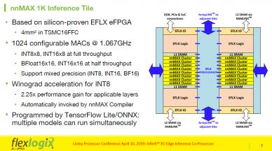
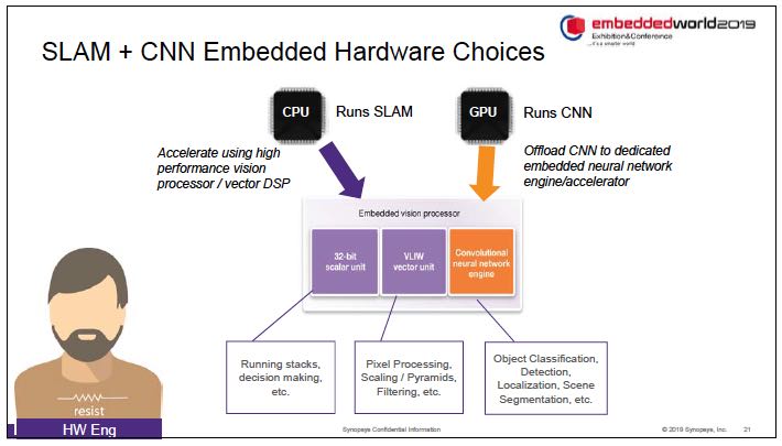
Inferencing customers needed large EFLX DSP MACs so a 1K nnMax tile was developed. A detailed look at the 1K configurable MAC Inference Tile shows the following architecture and features.
Winograd acceleration [SUP]1[/SUP] for INT8 provides 2.25x performance gain for applicable layers and is invoked automatically by nnMax compiler. The Tile is also programmed by TensorFlow Lite/ONNX with multiple models running simultaneously. The 1K tiles can be configured in any array size with configurable L2 SRAMs supporting 1-4 MB per tile and with a variable DRAM bandwidth through reconfigurable I/Os typically connecting x32 or x64 LPDDR4. The key advantage here is the ability to reconfigure ports and controls for the data path for each layer, and once configured, can run with ASIC-like performance, with routing to the memory and to interconnect, and with localized data access and compute.
Winograd acceleration speeds up 3×3 convolution with a stride of 1 by a factor of x2.25. Though the resulting architecture creates 2x larger weights and a more complex data path, nnMax performs the transformations on the fly, removing the weight penalties. Winograd is essentially free to the user from the performance perspective because they do not get any penalty in DRAM power or precision, but not free in hardware with only some additional bits in the multiplier.
Some layers have large intermediate frame sizes that may not fit in on-chip SRAM (e.g. YOLOv3 layer 0 outputs 64MB), resulting in DRAM writes and re-reads, putting a strain on DRAM bandwidth and potentially causing pipeline stalls when those layers are processed. To address this, multiple layers are run in parallel. In the YOLOv3 situation, Layer 0 and 1 are run simultaneously, avoiding the 64MB need to store with Layer 0 streaming directly into nnMax clusters processing Layer 1.
InferX X1 applications include edge devices such as surveillance cameras, robots, set-top boxes, edge servers like edge gateways and low-end edge servers.
The InferX X1 Edge Inference co-processor which runs at 1.067GHz on TSMC16FFC is scheduled for Q3 2019 tape-out with 8.5 TOPs, with 4K MACs, 8MB SRAM, x32 LPDDR4 DRAM, x4 PCIe Gen 3/4 lanes. Total dynamic worse-case power for YOLOv3, the most demanding, on PCIe Card, and including DRAM and regulators is 9.6W. InferX X1 silicon and PCIe cards will sample by the end of 2019. The typical power is 2.2 Watts on ResNet-50, and varies by model.
InferX X1 throughput is 3 to 11 times existing edge inference ICs and can be chained for higher inference throughput. Performance gain is greater on large models such as YOLOv2, v3. Furthermore, its throughput/Watt is 4 to 26 times better allowing edge devices to stay within their power budget.
The nnMAX compiler front-end flow performs the Neural Network model to soft-logic translation. The back-end flow performs place-and-route, retiming, pipelining and binary generation. The compiler first estimates performance, then accepts the X1 floorplan and TensorFlow Lite (soon ONNX) and automatically partitions the model across multi-layer configurations and computes performance, latency, MAC utilization, DRAM bandwidth per layer and per model.
During the panel discussion Dr. Wang was asked about complexity perception, he stressed that the architecture is simple, and the verification is not any more difficult than verifying an FPGA design. When asked about the memory requirements, he stated that since there is no way to store all parameters into SRAM in edge devices, you can try to train the model to be sparse or partition it over multiple devices. Certain aspects can also be serialized across multiple devices. When asked about the time it takes to reconfigure the fabric, the answer was about 1 microsecond per layer, allowing for a video processing 30 frames per second, with a model having 100 configurations, cycling through 3,000 configurations, 300 microseconds per layer and thus the user will not experience a drop in performance with, as designed, an acceptable hardware impact and complexity. When asked how one addresses models other than CNN, he said that embedded FPGA runs a lookup table from anything to anything. Most functions are not throughput intensive enough and FPGAs handle these beautifully. The activation function is all in the lookup table. Most functions have matrix multiplication or data movement and FPGAs are optimized for that. How you deliver enough bandwidth at the edge, when GDDR or HBM are not in the cards, was the reason why the architecture was designed the way it was so that not much DRAM is required.
Edge application is all about efficiency, and how much throughput one can get for a certain amount of power and certain amount of cost. The goal is to extract as much performance as possible and their solution is as close to a data center in performance while still in edge space. FPGAs typically have a problem with capacity because they try to map everything at once. Flex Logix has multiple configurations addressing the capacity issue where a certain amount of resources is required to map a model, with the compiler making decisions on how to multiplex data and what degree of parallelism to use based on how much resources are available and how much the model requires.
Geoffrey Tate, Flex Logix CEO, emphasized the ability of the reuse of their FPGA technology to deliver very high throughput inference capability for the more challenging models that the customers want to run at low power and low cost. The chip customer programs ONNX or TensorFlow Lite models and Flex Logix software takes care of the FPGA internals. The interconnect technology can reconfigurably program the non-blocking paths from memory on-chip through the hardware units like the MACs and back to memory giving much more efficient computation than other processor architectures.
___
1 Distinct from the conventional convolution algorithm, Winograd algorithm uses less computing resources but puts more pressure on the memory bandwidth. Flex Logix architecture mitigates that.