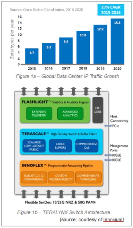
 The surge of network traffic at the data centers has driven to an increase in network bandwidth, doubling every 12-15 months according to a study conducted on Google’s data centers. The primary drivers to this uptick include the proliferation of cloud computing, more distributed storage architecture, emerging applications in AI, 5G and video streamings.
Innovium is a provider of high performance and highly scalable switching silicon solutions for data centers. Its TERALYNXTM Ethernet Switch family supports switch capacity ranging from 3.2 Tbps through 12.8 Tbps with large buffers. Key to its network switch design requirements are the power efficiency in terms of performance per watt, a very low latency and inherently high port count connectivity. Innovium has rolled-out several generation of silicon starting with 28nm at 3.2Tbps and the most recent one in 16nm at 12.8Tbps. One of the main challenges to its silicon design is the need to reduce the physical verification time.

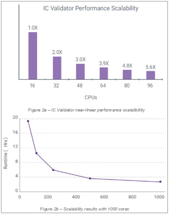
IC Validator™ is a comprehensive physical verification solution from Synopsys. It delivers both performance scalability and a broad runset support for advanced process nodes including 7nm FinFET. IC Validator’s Design Rule Checking (DRC) and Layout Versus Schematic (LVS) physical verification engine has near-linear scalability performance across hundreds of CPU cores and substantially reduces the time to results as shown in Figure 2.
Earlier this month, Synopsys announced Innovium adoption of IC Validator as its TERALYNX physical signoff tool. Innovium was able to take advantage of IC Validator’s performance scaling across 250 plus CPU cores to complete full-chip DRC/LVS signoff in TSMC 16 FinFET process within a day.
“Physical verification is on the critical path to our tapeout. Early physical verification closure is essential to ensure that design schedules are met,” said Keith Ring, vice president of Technology at Innovium. “IC Validator performance enabled us to complete full-chip DRC and LVS signoff within a day for our flagship network switch design.”
“Designers are challenged to close physical verification within schedule because of the increasing manufacturing complexity at advanced technology nodes,” said Christen Decoin, senior director of business development, Design Group at Synopsys. “Through high performance, scalability, and readily available optimized runsets from all major foundries, IC Validator is providing designers with the fastest path to production silicon.”
I had the opportunity to talk about this announcement with Manoz Palaparthi, Synopsys Technical Marketing Manager. The following is his excerpted responses to my inquiries:
What types of challenges that Innovium overcame by migrating to IC Validator physical signoff?
 Performance was a key concern for Innovium. The design is large with several billions of transistors to verify. As such, the traditional full-chip DRC signoff happens late in the design flow and its long runtimes can lead to tapeout delays. With IC Validator, Innovium could complete full chip DRC and LVS runs under one day. Innovium used IC Validator across more than 250 CPU cores to take advantage of IC Validator’s distributed processing and scalability.
Which parts of IC Validator verification features being utilized by Innovium?
Innovium deployed IC Validator for all of their physical verification needs, including DRC, LVS, Antenna checks and metal-Fill.
Could you comment on how IC Validator smart memory-aware load scheduling and balancing technology work?
Yes. The memory aware scheduling and smart load sharing technologies are built into the IC Validator scheduler.
Memory aware scheduling enables jobs to be scheduled based on their individual memory requirements. IC Validator scheduler estimates memory needs in advance. If a job requires large memory, for example 512GB or 1TB, it is scheduled on a large machine. Lighter jobs are scheduled on smaller machines. And as the jobs progress, the tool dynamically adjusts and reschedules as needed. With smart load sharing technology, IC Validator continuously monitors jobs and dynamically optimizes them: are the jobs progressing well? Have some machines died? Is load balancing and rescheduling required from some jobs?
Once the jobs start running, scheduler ensures that jobs run as efficiently as possible. This technology, combined with massive distributed processing scalability, accelerates time to results for customers like Innovium.
IC Validator has evolved to a comprehensive physical signoff tool, could you comment on how you keep adding values to the tool?
The focus for IC Validator product is on delivering highest productivity to the physical verification engineer. In that direction, we recently introduced lot of technology to help our customers to get to their tapeouts faster: Massively parallel distributed processing with scalability to 1000s of CPUs, Explorer to quickly identify and fix gross design weaknesses during chip integration and fusion technology for automated DRC repair, timing aware metal fill and more.
For potential users who would like to migrate to IC Validator, could you share what the expected pre-adoption collaboration time?
Potential customers can migrate to IC Validator very quickly. IC Validator runsets are readily available for all mainstream process nodes from foundry partners such as TSMC, GF, Samsung and more.
After the runsets are ready, it is just a matter of few hours to setup the tool and start running PV jobs with IC Validator. Over the next few days/weeks, customers typically do runs with some designs to evaluate tool for performance and features. Several of our recent customers are able to deploy IC Validator in production within a month.
To find out more details on IC Validator, please check HERE
Share this post via:


Comments
One Reply to “Switch Design Signoff with IC Validator”
You must register or log in to view/post comments.