AI, Machine Learning, Deep Learning and neural networks are all hot industry topics in 2019, but you probably want to know if these concepts are changing how we actually design or verify an SoC. To answer that question what better place to get an answer than from a panel of industry experts who recently gathered at DVcon with moderator Jean-Marie Brunet from Mentor, a Siemens business:
Continue reading “Deep Learning, Reshaping the Industry or Holding to the Status Quo”
Semiconductor Equipment Revenues To Drop 17% In 2019 On 29% Capex Spend Cuts
The semiconductor equipment market grew 37.3% in 2017 on the heels of capex spend by memory companies in order to increase bit capacity and move to more sophisticated products with smaller nanometer dimensions. Unfortunately these companies overspent resulting in excessive oversupply of memory chips. As memory prices started dropping, these companies put a halt to capex spend, and global equipment revenues increased only 13.9% in 2018. As excess inventory continues to increase in 2019, capex spend by these companies is projected to drop 29%, which will result in a significant reduction in equipment revenues in 2019.
As a result, the global semiconductor equipment market is forecast to drop 17% in 2019, reaching revenues of $64.5 billion, according to The Information Network’s report, “Global Semiconductor Equipment: Markets, Market Shares, Market Forecasts.”
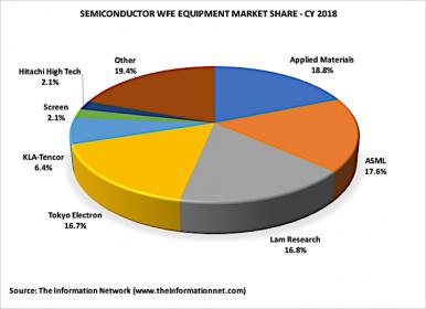
To analyze the equipment market in 2019, we need to look at revenues and market shares for previous years. For 2018, Applied Materials (AMAT) ended the year with a market share of 18.8%, down from 21.2% in 2017, as shown in Chart 1. Fellow U.S. supplier Lam Research (LRCX) held a 16.8% share in 2018, down from 16.9% in 2017.
Japanese supplier Tokyo Electron Ltd. (OTCPK:TOELY), a major competitor of AMAT and LRCX in the deposition and etch sectors, held a 16.7% share in 2018, an increase of 1.6 points from a 15.1% share in 2017.
Chart 2 illustrates the change in revenue YoY for the leading semiconductor equipment companies. As I said above, the overall market increased 13.9%, so Lam’s growth of 13.7% attributed to its 0.1 point loss in share. AMAT’s lackluster growth of only 1.1% in 2018 contributed to its loss of 1.6 share points. Growth was less than the composite growth of companies ranked 8 through 75. The company has been losing market share to competitors YoY for the past three years.
KLA-Tencor (KLAC) grew 26.1%. I noted in a January 31 Seeking Alpha article entitled “KLA-Tencor And Metrology/Inspection Peers Will Be Less Impacted By Memory Capex Cuts Than The Rest Of The Equipment Industry In 2019” that a shift to more inspection in the fab was underway.
AMAT sells equipment for nearly all the processes used to make a semiconductor chip. Its two major segments are deposition and etch. In 2015-2017, deposition made up 46% of AMAT’s revenue, while etch made up 18-20% of revenues. These two sectors represent 2/3rd of the company’s revenues.
In 2018, the deposition market grew 3.9% and etch grew 4.4%. Since AMAT’s total revenues grew just 1.1%, it is obvious that the company lost shares in both sectors to competitors in these sectors, namely Lam Research, Tokyo Electron, and Hitachi High Technologies (OTC:HICTF).
2019 Analysis
Based on capex spend data as detailed in Table 1, The Information Network projects the semiconductor equipment market will drop 17% in 2019, compared to growth of 13.9% in 2018.
The main reason is the drop in capex spend by memory companies tied to the inventory overhang and oversupply of 3D NAND and DRAM chips. In total, capex spend is projected to drop 29.1% in 2019.
But there is another important factor investors need to consider: market share gains and losses. Why are market shares important?
Semiconductor manufacturers purchase equipment based on a “best of breed” strategy. Market share losses indicate equipment is not best of breed. When a customer decides to make additional equipment purchases to increase capacity, it will buy more from its current supplier. This means further market share gains.
A Brief History of IP Management
As RTL design started to increase in the late 1980’s and early 1990’s, it was becoming apparent that some amount of management was needed to keep track of all the design files and their associated versions. Because of the parallels to software development, design teams looked to the tools and methodologies that were in use by software teams at the time.
Software teams had adopted Software Configuration Management solutions to handle the organization and versioning of their source code. RCS and CVS were two of the most popular revision control systems in use at the time, and semiconductor development teams began to adopt these for their development environment, eventually building methodologies around the use of these solutions.
It quickly became apparent that the differences between hardware and software design necessitated that more customized solutions needed to be developed for the semiconductor development teams. Binary databases for analog design needed to be supported, integration into the EDA environment were needed, and support for scripting and configuration files for EDA tool flow had to be developed.
In 1993, the consulting group at VIEWLogic began work on providing the first such environment for hardware teams. Building on top of RCS, they released ViewData, a plugin for the PowerView framework. This solution began to address the needs of managing configurations of files where RTL, schematics, and layout all made up the final design configuration.
In 1995, Dennis Harmon, Mitch Mastelone, Norm Sozio, and Eugene Connolly left VIEWLogic to form Synchronicity with the goal of providing the first true semiconductor design data management system that would manage design data across different development platforms and EDA tool environments. In 1996, they released DesignSync, which was built on top of a custom data management system that could handle the RTL and other ASCII data, and connectors into the solution that would interface with the EDA tools at the time. This solution became popular with analog designers, as now there was a way to handle the binary data and custom frameworks associated with Analog design.
Two years later, Srinath Anantharaman founded ClioSoft to continue to fill in the gaps that were not met by software SCM tools. ClioSoft launched the SOS design collaboration platform to target the challenges of hardware design. Like DesignSync, ClioSoft built SOS on top of a customized data management system, and developed technology to augment the traditional SCM approach to create a hardware configuration management (HCM) system while partnering with EDA companies to provide specific connectors into the EDA tools and methodologies.
In the ensuing years, there was a rise in the development of commercially available data management (DM) platforms. IBM Rational’s ClearCase and Perforce’s Helix were being adopted by development teams in many different industries. A new generation of open source solutions were also being developed, such as Subversion and later, Git. This allowed for a second generation of solutions to be introduced to the market that allowed for the adoption of solutions that were built on top of these commercially available solutions instead of running on proprietary data management systems.
In 2003, Shiv Shikland and Dean Drako founded IC Manage. Building on top of Perforce’s Helix data management solution, they released their Global Design Platform (GDP). By choosing to release their solution on top of a commercially available DM system, design teams were able to use a common DM system for software and hardware design, with the GDP client able to be customized for the needs of hardware designers.
Four years later, Simon Butler and Fergus Slorach founded Methodics. Methodics also chose to run on top of commercially available systems, but instead of limiting the solution to a single platform, they chose to allow users to run their choice of platforms, with Perforce and Subversion being the two most popular at the time. This further allowed customers to mix and match backend DM systems to fit their needs while having a common client, VersIC, running on top of the different systems for hardware design.
As design reuse began to gain traction in the early 2000’s and the use of third party IP began to grow, semiconductor designers were now faced with the challenge of managing designs for reuse, and managing the acquisition of third party IP. Design teams needed to know where to find internal IP for reuse and be able to track what versions were being used, in which projects it was being used in, and what products had taped out with what versions of IP. Third party IP complicated the problem, as each IP acquired often had a different contract that stipulated how the IP provider was to be paid for the IP’s use. Often, users of this IP would have to keep track of varying business terms that required the users to keep track of who looked at the IP, was it uses once or many times in a design, how many different designs was it used in, or how many parts were ultimately shipped after tape out.
Semiconductor design teams looked to the design management companies to provide solutions in this area. Synchronicity was first to market in the IP management space with IP Gear, Methodics released ProjectIC, IC Manage developed IP Central, and ClioSoft released DesignHub. Later, in 2004, Synchronicity would be acquired by MatrixOne, developer of one of the first PLM systems, to bring semiconductor design management closer to systems development. MatrixOne would then be acquired by Dassault Systemes in 2006. While DesignSync lives on as part of the ENOVIA PLM group in side of Dassault, IP management has been integrated into the ENOVIA PLM platform itself. Methodics has release Percipient as a follow on to ProjectIC, incorporating an IP LifeCycle Management (IPLM) methodology into the solution and providing integration to other engineering systems like requirements management and issue and defect systems.
Today, SoC’s continue to take advantage of reuse, with the number of IP cores in an SoC exceeding 100. The challenges facing the management of IP are still increasing. Functional safety requirements, such as ISO 26262 for automotive and DO-254 for aerospace, push semiconductor companies to provide evidence of a traceable path from requirements through design to verification and to document all work that has been done to meet those requirements. The need for these traceable flows require that IP management systems have links into requirements, verification and document management systems. Increasing use of third party IP are making designers look for robust IP portals with abundant IP meta data available so that they can accurately compare IP from different vendors. With the industries dependence now on IP, IP management systems will remain core to the effective collaboration of design teams for the years to come.
Also Read
Three things you should know about designHUB!
Foundational Excellence in a Laid-Back Style
I recently had a call with Rob Dekker, Founder and CTO of Verific. If you’re in EDA or semiconductor CAD, chances are high that you know who they are. They’re king of the hill in parser software for SystemVerilog and VHDL. When you hear a line like that, you assume a heavy dose of marketing spin, but here it really is fact. I don’t know of anyone else in this line with their market presence. They’re used by all the EDA majors and by CAD groups in leading semiconductor and systems companies (Intel and Google, to drop a couple of names).
I have some familiarity with this space since I was for a short time in Interra Systems before we spun out as Atrenta, and Interra provided our Verilog and VHDL language parsers. I don’t know about the business side of that activity but I do know we were always struggling to keep up with the standards and, more challenging, vendor-specific wrinkles on those standards. When you’re low in the EDA value chain and you’re using your own parsers, that’s a constant headache in competing with the big tool providers. Using Verific for parsing eliminates those headaches and lets you focus on your differentiating value-add.
I asked Rob what got them started on this path. He had been responsible for language front-ends for the Exemplar logic synthesis software back in the 1990s. In 1999, after Exemplar was acquired by Mentor Graphics, he decided to start his own company. He was originally thinking about developing a formal verification tool (hence the name Verific), but of course had to start with language parsing and RTL elaboration, the front-end to any formal tool. So he built that and found several customers who were interested in licensing that software.
A couple of years later, a company developing an equivalence checker approached him wanting to license the parsers. That was one of those defining forks in the road for a small company – if he continued along the path he originally planned, we would be competing with a customer. Instead he decided to stay in the parser business but do the very best he could in that domain. The formal company became a customer and fairly quickly after that most formal providers were using Verific parsers.
The business model is a little unusual but seems to work well for them and for their customers. They were clear from the outset that they wanted to be in the (software) IP business, not the services business, but that they would license source-code rather than compiled libraries. Customers can build on their favorite hardware/OS platforms, as best suits their needs. Of course if you have source code, you can change it. The model here seems to be that you’re likely only to make minor tweaks. Verific will support these changes, merging them on top of a standard release and re-regressing with their test suites before release back to the customer. Rob says that customers like this model. In the event of something bad happening to Verific, customers already have hands-on experience with the source-code, a possibility which remains theoretical in most software license agreements.
The pricing philosophy is equally simple; this has to be 50% of what the customer thinks it would cost them to develop. Customers are always optimistic when they do this calculation. So the real percentage has to be 25% of Verific’s development cost, which means they have to sell 4 copies before they start to make money. Turns out that their customers find this very reasonable, so they don’t run into a lot of resistance.
You’re probably wondering about the available market for products like this. Rob said that they originally mostly targeted EDA developers, for formal, synthesis, some simulators, hardware accelerators, even virtual prototypers. The Verific software is built in C++, with C++ interfaces, so is a natural fit for that type of development. They still find some new business in this area but have seen more growth over time in semiconductor CAD groups, in traditional semis and in design groups in the big systems houses. There’s still need for a lot of custom tooling in these groups and Verific provides a good turnkey front-end to RTL analysis.
However, in-house CAD groups are generally not as enthusiastic about C++ development; their development languages of choice tend to be Python or Perl. Verific’s first pass at meeting this need was to wrap underlying C/C++ APIs for these languages. I’ve been there, done that so can sympathize with Rob’s statement that this didn’t help so much. APIs for these kinds of applications tend to be overwhelming. You can do anything you want to do, but it takes forever to figure out how. In 2017 Verific solved this problem by acquiring the INVIO platform from Invionics. INVIO builds on top of the basic APIs with a much simpler object-based model and the kind of lookup functions you’d expect to have in a Tcl interface. I’d imagine this is a big hit with CAD developers and probably even with designers.
Asking Rob about long-term goals, I got an answer you’d never hear in Silicon Valley, perhaps because this is a company with strong European roots. Rob feels they are in a good niche market; they are already the industry standard with little competition, they like where they are and don’t feel the need to grow too fast. Which is just as well, because he doesn’t see massive room for growth. They have been able to manage double digit growth each year, which is fine by them, helped along now and again by a new parser, such as a recent introduction for UPF.
In an industry where CAGRs must be spectacular and competition is a blood sport, this is a refreshing change. Rob told me the reason they chose a giraffe as a logo was that it has a good overview of its surroundings, but at the same time has a gentle and non-aggressive nature both internally and with partners. Quality of life as a primary goal – an interesting differentiator.
Rambus Take on AI in the Era of Connectivity at Linley Processor Conference
Steven Woo, Fellow and Distinguished Inventor presented at the just concluded Linley Spring Processor Conference a talk about AI in the Era of Connectivity. As he put it, the world is becoming increasingly connected, with a marked surge of digital data, causing a dependence on said data. With the explosion of digital data and AI, the interaction is such that they are feeding off each other. Consequently, architectures are evolving to more efficiently capture, secure, move, and process the growing volume of digital data.
Data Centers are evolving, and data processing is moving to the edge. Data is increasingly valuable and sometimes more so than the infrastructure itself so securing this data is essential. Power efficiency is also a key consideration. There is an interesting evolution/revolution in how data is captured, processed and moved. AI techniques have been around for decades, so why the sudden resurgence of interest? Faster compute and memory along with large training sets have enabled modern AI. With the transistor feature size limits being reached and the increased need for performance coupled with energy efficiency mandates, clearly new approaches are needed and indeed emerging.
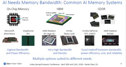
AI relying on CNN (convolutional neural network) is suddenly taking off due to its increasing accuracy as the data and the model size increase. To support this evolution, Domain Specific Architectures (DSAs), have emerged with specialized processors targeted specifically for some tasks away from general purpose compute. Memory systems are critical in these systems and can range from On-Chip Memory to High Bandwidth Memory (HBM) and GDDR. On-Chip Memory provides the highest bandwidth and power efficiency, with HBM exhibiting very high bandwidth and density, while GDDR sits in the middle and provides a good trade-off between bandwidth, power efficiency, cost and reliability.
With Data growing in value, security is challenged by increased sophistication of intrusion attempts and exploitation of vulnerabilities. The surface area to attack is also growing due to infrastructure diversity, pervasiveness and user interaction type, with the spectreof a meltdown foreshadowing, pun notwithstanding, more havoc to come.
Rambus has a new approach called Siloed Execution that improves security where physically distinct CPUs separate secure operations from other ones that require fast performance. The security CPU can be simplified and armored for tighter security for secret keys, secure assets and apps, and privileged data, remaining uncompromised even if the general-purpose CPU is hacked. Rambus has such a secure CPU, the CryptoManager Root of Trust which provides secure functionality for secure boot, authentication, run-time integrity and a key vault. It includes a custom RISC-V CPU, secure memory and crypto accelerators such as AES and SHA. With a secure CPU integrated on the chip you can monitor run-time integrity in real time in the system and make software/hardware adjustments as needed.
The AI infrastructure connection is helped by allowing cloud shared neural network hardware to be used by multiple users who can now encrypt their training sets and even their models and the security CPU can manage different keys to decrypt that information for each user. Rambus’ CryptoManager Root of Trust would allow a multi root capability, with a key decrypting one user data, allowing access to the model parameters for training and inference, then a second user can have their data decrypted with a separate set of keys and run on the same hardware.
On the memory side there is a wide range of solutions available that are appropriate for some applications with no one size fits all and on the security side the data itself is becoming in some ways more valuable than the infrastructure. It is important to not only secure the infrastructure but also it is important to secure the training data and models as it can be your competitive advantage. Over time, what will be needed is allowing the user to have simpler ways to describe their models by using compilers to transform something that is hard to describe to the user but that runs extremely well on hardware. What is needed is how to describe the job and less and less will be needed on how neural networks work and software will enable this transformation over what the latest available hardware provides.
Dr. Woo stressed that AI is driving in a sense a computer architecture renaissance. Memory systems now offer multiple gradations of AI options for data centers, edge computing and endpoints. As the data value is increasing, with growing security challenges, security by design is imperative as complexity and data grows with no sign of slowing down. If you get AI, then get security, and get going with functional integration and task separation, all in one AIdea. Sounds like a good name, get the AIdea?
IC Implementation Improved by Hyperconvergence of Tools
Physical IC design is a time consuming and error prone process that begs for automation in the form of clever EDA tools that understand the inter-relationships between logic synthesis, IC layout, test and sign-off analysis. There’s even an annual conference called ISPD – International Symposium on Physical Design, and this year it was held in San Francisco, April 14-17. For the keynote speaker this year they invited Shankar Krishnamoorthy from Synopsys to talk about, “Fusion: The Dawn of the Hyper Convergence Era in EDA“. I was able to review his presentation to better understand the challenges and EDA approach that Synopsys has undertaken.
Before I delve into EDA tools, let me first take a step back and review what’s happened in the datacenter recently, where three mostly separate technologies have morphed into a single, more optimized system (aka hyperconvergence):
- Computation
- Storage
- Networking
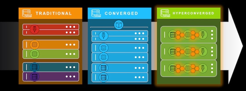
So a hyper-converged infrastructure (HCI) uses software and virtualized elements running on commercial, off-the-shelf servers to improve performance and enable easier scaling. In the traditional datacenter server the networking could come from Cisco, the compute by HP and storage by EMC, but the setup and maintenance was complex, a bit inefficient and scaling was brute force.
By the 2010’s we saw datacenter servers take a converged approach where either Simplivity and HP partnered, or EMC and Dell partnered, so it was easier to manage than the traditional data center but still had issues with limited capabilities and reliability.
Since the mid 2010s we now see the emergence a hyperconverged datacenters with vendors like Nutanix that have fused together the once separate components of storage, compute, networking and virtualization.
I’ve been an EDA tool user since 1978 and blogging about EDA tools for over 10 years, so I’ve seen many generations of tools being offered. Through the 1990s we saw many CAD groups combining multiple point tools into a traditional flow for nodes down to 90nm, as shown below. Sure, you could mix and match the best tool for each task, yet there would always be iterations to reach closure.
The converged approach has been in use since 2000 and used on IC implementation down to 7nm, with EDA vendors typically providing more integration and links between the tools. Benefits with a converged approach are more coherency, and an improvement in predictability, but the sheer size of IC designs and unprecedented complexity due to relentlessly advancing Moore’s Law have made even this methodology unviable.
Going from RTL code to signoff while meeting the QoR and productivity targets is a much bigger task at 7nm and below, so creating an EDA tool flow to meet this challenge could take a couple of approaches: Loose coupling between multiple engines using separate data models, or a single data model with common engines.
Loose coupling between engines
With a loose coupling approach between engines there’s still an issue meeting PPA (Power, Performance, Area) and convergence, because you don’t always get a predictable improvement over time, and the runtimes are lengthened because there are still iterative recipes being used.
The hyperconverged “Fusion“ approach is distinguished by a single data model, single user cockpit and common interleaved engines:
The promise of this approach is a quicker convergence to optimal PPA. Just think about how an end-to-end physical implementation system unified on a single data model and using common synthesis, place-and-route and signoff engines could enable seamless optimization throughout the flow for superior QoR and signoff predictability:
OK, the theory of hyperconverged EDA tools sounds interesting, but what about actual results? One IC design with 2.5M instances and 5 power domains using a 16nm process was run in both converged and hyperconverged tools, showing the following improvements:
- 2.4X faster full-flow turnaround time
- 46% better timing
- 11% less area
Engineers love data, so here are some more results using the hyperconverged approach on multi-million instance designs at 16nm and 7nm process nodes:
- Mobile CPU
- 10% Total Negative Slack (TNS) improvement
- 10% Leakage improvement
- 3% Smaller area
- Automotive IC
- 28% TNS improvement
- 13% Smaller area
- High performance server SoC
- 56% Leakage reductions
- 41% Faster runtime
- 10% Smaller area
So this new hyperconverged Fusion approach from Synopsys uses many common optimization technologies throughout the flow to concurrently optimize across multiple metrics, including timing, power, IR drop, area and congestion. For instance, by using an integrated IR analysis engine in the flow it can resolve IR violations without impacting timing closure, look at one comparison versus the baseline flow:
The baseline flow had 3,136 IR violations where the threshold was >=8% IR drop, while the Fusion flow had just 137 IR violations, that’s a whopping 95% reduction with the newer approach.
Summary
If you use the same EDA methodology from a 28nm flow on a 7nm or 5nm SoC, then there are going to be some big surprises as you iterate and attempt to reach an acceptable PPA value within the time budget allotted. Change with the times and consider the hyperconverged approach being offered by Synopsys in Fusion, the early numbers looked promising to me.
Customizing and Standardizing IP with eSilicon at the Linley Conference
During the SoC Design Session at the just concluded Linley Spring Processor Conference in Santa Clara, Carlos Macian, Senior Director AI Strategy and Products at eSilicon, held a talk entitled ‘Opposites Attract: Customizing and Standardizing IP Platforms for ASIC Differentiation’.
Standardization is key to IP in modern systems-on-chip (SoC), yet without customization a huge amount (of revenue, performance, area optimization) is left on the table. The spectrum of standard to custom IP goes from common functions turning into standard IP which could evolve into an IP platform that transforms into what eSilicon terms an ASIC chassis and finally consisting of customized IP.
A recent customer design, a machine learning ASIC, included a large amount of IP from 400Mb of embedded SRAM, 48 lanes of 28G SerDes, PCIe SerDes, HBM2 PHY, custom and compiled memories, PLLs, eFuse, analog, PVT monitors to name a few. Standard IP is the opposite of having your special secret sauce, but it is critical to your schedule, cost and efficiency. In a typical 7nm Data Center chip these days, 40-50% of the area and power of the ASIC is related to the IP, 30-50% of the unit cost depends on the IP, before even accounting for royalties. And 30-50% of the NRE development cost is due to IP-specific NRE and is the single highest cost after the mask tooling for 7nm. It is also more expensive than the total design labor cost from RTL to tape-out.
In addition, there is the effort needed in IP integration from test and bring-up to integration/verification interface and interaction with providers. The IP may not be as critical as your secret sauce solution, but it needs to be as cost efficient, as easy to integrate and test and as power/performance/area efficient as you can possibly get. When IP is used, the number one goal is to reduce or eliminate the development and integration effort for the parts of the design that are not critical.
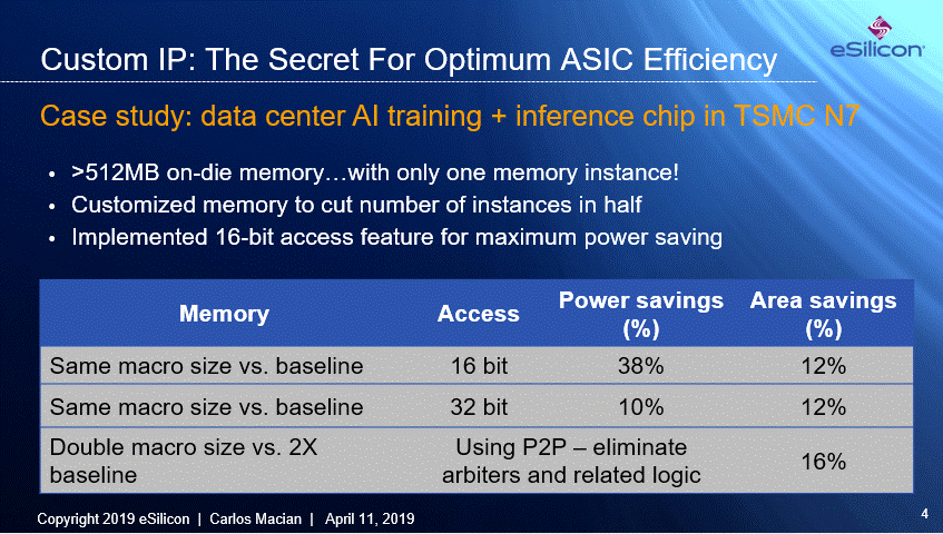
How do standards help? Common interfaces help in interconnectivity and shared functionality allowing easy integration and less interoperability disconnects. Deliverables in standardized form also simplify the tasks. Beyond standardized IP, platforms enable the harmonization of various IPs, so they work well together for a particular node or a market niche. Verification is always needed and for certain applications there is commonality in desired functionality and deployment, and templates can greatly facilitate the deployment and implementation with cost and time savings. IPs, by definition, include overhead since not all use cases have the same functional features, so a common denominator of sorts injects additional circuitry to cover all bases. So, customizing to the needed features can end up saving a lot of power and real estate. Trimming unneeded memory is one example of customization that pays dividends.
Carlos Macian closed with stressing that IP matters, and in summary, using standard IP for standard consistent results, in conjunction with custom IP to increase your market advantage be it through features, performance, power, area, though opposite in means ,are synergistic in ways, the ways of optimal design practice for timely market success at desirable customer value.
During the Panel discussion at the end of the session, Carlos Macian was asked about eSilicon’s approach to pre-verifying. His approach was to verify the RTL, then netlist operation, followed by the other dimension of going beyond the standalone functionality and verifying the integration with the cores which cannot of course be pre-verified, and that is only possible towards the end when the implementation is complete and this is the responsibility of the customer. But at all the levels, the cycle of verification is stream-lined and more straightforward. Silicon verified IP blocks are mandatory to increase the functionality confidence factor. On the AI front, building blocks are provided to generate the AI tiles. The difference between inference and training is going to affect the functionality you place in the AI tile, but it does not affect what is around it such as the ASIC chassis. When asked about the RISC-V value proposition, eSilicon believes that RISC-V facilitates integration greatly, however other processors are also used in its solutions.
The neuASIC [SUP]TM[/SUP] Platform provides compiled, hardened and verified 7nm functions, greatly simplifying the design imperatives providing fixed functions and streamlined data flow architectures. One of the reasons we are seeing hesitation to optimize to the last degree all the systems is due to the fact the field is evolving rapidly. The semiconductor community at large is conservative and risk averse given the multimillion-dollar cost of advanced silicon nodes, so we are seeing that certain workloads are becoming more mature, better understood and more prevalent. While discovering new workloads and new network models that address those workloads, as those mature workloads are better understood, the incentive of building optimized implementations that will scale extremely well for a larger user base, becomes more attractive. For the newer workloads being discovered, programmability plays a key role, modern accelerators are providing programmability such as RISC-V processors, while sitting next to hardware optimized solutions.00
As far as the deliverables are concerned, the standard list from Verilog model to GDSII, test benches, integration guidelines, data sheets, timing constraints, silicon reports since eSilicon is providing hard IP. The integrity of the overall solution is covered given the eSilicon ASIC heritage, knowing where potential interoperability issues arise, and ongoing communications with the customers occur to make sure their functionality is assured as best as possible. Best in class IP is no longer enough, it is compatible IP and it is an architecture that allows the IP to work together that is in order. Programmability and configurability such as compilable memory provide customization. Configurability is also in the SerDes, with parameterized control in the transmit and receive channels.
IP integration in the ASIC matters and IP customization matters. In order to differentiate your product, you need to take advantage of those two aspects and bring out the value in both dimensions.
User2User Silicon Valley 2019
This will be one of the more interesting Mentor User Group Meetings now that the Siemens acquisition has fully taken effect and the new management team is in place. The Mentor User Conference is at the Santa Clara Marriott, Santa Clara, California on May 2, 2019 from 9:00 am to 6:00pm.
Remember, in 2017 Siemens acquired Mentor Graphics for $4.5B representing a 21% stock premium. Acquisition rumors had been flying around the fabless semiconductor ecosystem but no one would have guessed it would be the largest industrial manufacturing company in Europe. At first the rumors were that Siemens would break-up and sell Mentor keeping only the groups that were part of Siemens core business, specifically they would sell the Mentor IC Group. Those rumors were flatly denied at the following Design Automation Conference during a CEO roundtable and now Mentor, including the IC group, is an integral part of the Siemens corporate strategy.
Last year Wally Rhines transitioned from Chairman and CEO of Mentor to CEO Emeritus. It’s not just an honorary title, Wally still spends 20% of his time at Mentor, mostly with customers. Joseph Sawicki is now in charge as the Executive VP, Mentor IC EDA, a Siemens Business. Everyone knows Joe, he has been with Mentor for close to 30 years and is a “leading expert in IC nanometer design and manufacturing challenges. Formerly responsible for Mentor’s industry-leading design-to-silicon products, including the Calibre physical verification and DFM platform and Mentor’s Tessent design-for-test product line, Sawicki now oversees all business units in the Mentor IC segment.” Not only that, Joe is a hellava good guy. I will be there for Joe’s keynote. If you see me please say hello, it would be a pleasure to meet you.
The event details and registration can be found here.
Join Mentor on May 2, 2019 at the Santa Clara Marriott in Santa Clara, California for User2User Silicon Valley, a one-day conference and exhibition dedicated to end-users of Mentor EDA/IC solutions. Admission and parking for U2U is always free and includes access to 45+ technical presentations, lunch, parking, end of day networking reception, and more! U2U gives you the opportunity to learn from and meet face-to-face with technical experts who design leading-edge products using Mentor tools. Stay all day and you’ll have a chance to win some fantastic prizes at the closing session!
U2U Silicon Valley is focused on these key areas
- Analog/Mixed-Signal Verification
- Functional Verification and Emulation
- Design-for-Test and Semiconductor Data Analytics
- IC Design and Verification
- High Density Advanced Packaging
- MEMS and Custom/Analog Design for the IoT Era
Keynotes
Joe Sawicki
Executive VP, Mentor IC EDA, Mentor, a Siemens Business
Vicki Mitchell
VP, Technology Services Group, IPG, Arm
Allen Sansano
VP Engineering, Wave Computing
Session Highlights
- How to Close Coverage 10X Faster Using Questa inFact – Microsoft
- Integrated Approach to Power Domain/Clock Domain Crossing Checks – Challenges and Implementation – Cypress Semiconductor
- Analog/Mixed-Signal (AMS) Design Challenges for high speed SerDes in nm-scale CMOS for 5G and Automotive Applications – Qualcomm
- Accelerating verification of high precision MEMS sensor SoCs with Symphony – Invensense
- Parasitic Extraction for GLOBALFOUNDRIES 22FDX-EXT PDK – GLOBALFOUNDRIES
- Enabling faster top-level DRC runtimes through targeted optimizations and Mtflex – Customer Presentation
- Maximizing Veloce Value for AI Design Verification – WAVE Computing
- SSD Controller Verification with Veloce Solutions – SK Hynix Memory Solutions
- What’s Driving Heterogeneous Integration and Which Packaging Option is Best? – TechSearch International
- Package Assembly Design Kits Bring Value to Semiconductor Designs – Amkor
- Improving Test and Fault Coverage with Tessent Cell-Aware Models using Artisan Physical IP Library – Arm
- An AI Chip DFT Design Flow for Catching Time-To-Market (Gyrfalcon) – Gyrfalcon Technology Inc.
- A Case Study of Testing Strategy for AI SoC (Enflame) – Mentor
- GLOBALFOUNDRIES 22FDX® Custom Design with Mentor Tanner Tools – GLOBALFOUNDRIES
- Supersede 5G – Gain Ics
- Accelerating AR/VR Computer Vision Algorithms in a Hybrid HLS/RTL Approach – Facebook
- In Depth Power Optimizations of Ultra Low Power STM32 Microcontroller with Nitro-SoC – STMicroelectronics
View the full conference agenda here.
U2U Exchange
Meet experts in the U2U Exchange, your hub for information, product demos, and technical advice. Share your experience and hear about the latest solutions from Mentor as well as featured partners. This year’s exhibitors include Arm, GLOBALFOUNDRIES, Samsung, TowerJazz, TSMC, and Oski Tchnology.
Auto Shows No Connection
The Washington Auto Show, one of the largest auto shows in the U.S., has a problem and it is a problem shared by other auto shows in the U.S. and around the world. It is a problem that plagues the entire industry and it may spell trouble for connecting with car customers.
I visited the Washington Auto Show last week. The event closed on Sunday. I visited with my wife who wanted to know more about vehicle connectivity services. I was skeptical that the personnel manning the booths at the event could answer my wife’s questions and my skepticism was validated.
There was not a single booth with adequate literature or exhibits to explain connected vehicle services. It seems like a trivial matter. It’s not. It’s a big deal.
More than 20 years ago General Motors defined the meaning of vehicle connectivity with the launch of OnStar – a cellular-based system designed to provide post-crash emergency response. In the event of an airbag deployment, the OnStar system will call the nearest public service access point (PSAP) to connect the car to a call center capable of arranging the dispatch of fire fighters, police or medical personnel.
The elegance of the OnStar service resides in its simplicity. OnStar has always done this one thing well and, at the time of its launch, actually came to be adopted by several competing auto makers as a critical, foundational application for a connected car.
GM ultimately terminated its OnStar licenses to other auto makers, some of which created their own OnStar-like systems. The European Union liked the idea so much it introduced an emergency call (eCall) mandate that went into effect about one year ago.
A lot has changed about vehicle connectivity since the time of OnStar’s launch. The cellular network changed from analog to digital, for one, enabling Internet access to cars.
In turn, GPS and embedded navigation have become widespread and now car makers are experimenting with digital assistants integrated with vehicle systems. In spite of these advances, though, car makers have yet to clearly define what vehicle connectivity is or means to consumers.
The strangeness of this failure arises from the fact that the automotive industry is on the cusp of a transformative change in vehicle connectivity. According to Strategy Analytics, 2019 marks the first year that more than 50% of new cars being shipped from factories globally will come with built-in wireless connections.
This reality will have escaped your notice if you attended the Washington Auto Show. Booth personnel were unfamiliar with the fundamentals of vehicle connectivity and most messaging beyond horsepower and cosmetics was focused on smartphone connectivity and safety systems. Even the electric vehicles, always a point of emphasis at the Washington show, were shown off primarily for their performance characteristics in an on-floor driving demo.
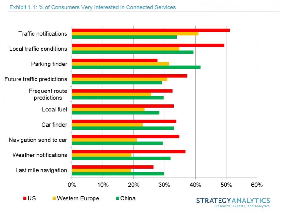
As far back as 2016, Strategy Analytics consumer research conducted in China, Europe and North America showed strong interest in embedded connectivity for a range of mission critical driving services.
My own shorthand for consumer interest in connected services is TWP – traffic, weather, parking. The list does need to be revised though, for 2019: TWPCS – as in, traffic, weather, parking, cybersecurity and software updates.
We have a major cybersecurity problem in the world today and connected cars are just one source of vulnerability. It may seem counter-intuitive but no car will be cyber-secure if it isn’t connected – though a connected car itself is vulnerable.
With millions of lines of software code embedded in most new cars supporting increasingly sophisticated safety and infotainment systems connectivity is a necessity. Yet consumer-focused car shows continue to neglect the vital messaging essential to educating the driving public.
The issue is even worse at dealerships. Vehicle connectivity ought to be seen as a means for reinforcing existing customer retention tools, but the average dealer sales person, with notable exceptions (BMW), is poorly trained on connected services and more inclined to tout smartphone connectivity to the average customer.
Conquering connectivity is a monumental task for the automotive industry. The world is poised on the threshold of a global roll out of 5G wireless technology designed to transform the fundamental nature of connectivity itself.
Cars will benefit mightily from 5G connectivity which will enable cars to avoid collisions in real-time while anticipating traffic light changes and being warned of road hazards ahead. Cars will be able to detect and prevent cyber attacks and receive vital software updates for navigation and safety systems.
There’s no excuse for car makers and their representatives to be incapable of accurately explaining connected vehicle systems and selling those systems to consumers. Horsepower and leather interiors are cool, but connectivity will save lives.
A Tale of Two Semis
It was the best of times (for stocks)
It was the worst of times (for memory chips)
The disconnect between stock & chip prices
The Venn Diagram of Stocks and Chips
Having been involved with semiconductor and tech stocks for a long time there has always been a loose correlation between the fortunes of the industry and the fortunes of the stocks, which varies over time. Right now we are in one of those periods where the Venn diagram has little overlap as the stocks have been on a tear while the industry wallows in the mud. Memory chip pricing and demand has been bad, to say the least and logic demand has not lit the world on fire as the whole smart phone industry has clearly slowed, led by Apple.
You don’t buy equipment when cutting capacity
With Micron cutting back on wafer starts by 5%, they are voting with their feet. A 5% cut back in wafer starts does not correlate to a 5% cut in equipment purchases. Equipment purchases are almost binary. In times of glut, such as we are in now, equipment purchases related to capacity go to zero, while equipment purchases related to technology slow. We doubt that Samsung or other memory makers are spending to build capacity as they also have too much.
A third order derivative market
We have said many times that higher order derivative markets are more volatile than first orders markets and semi equipment is a third order derivative market;
- Smart phone & consumer sales slow – sneezes
- Semi market sees memory crater – catches a cold
- Semi Equip memory sales go to zero – gets pneumonia
Life at the end of the food chain is always more volatile.We saw it in the up cycle and we are seeing now in the down cycle.
The “new normal” is likely lower than the “old normal”
The chip industry went through a “perfect storm” of circumstances that is not likely to be repeated when the industry recovers. The industry, in the last cycle, was driven by moving from rotating media to SSD’s, conversion from 2D to 3D memory, multi patterning due to the lateness of EUV, among others among factors, all of which are one time events that will not be repeated.
This most recent up cycle was higher than normal due to these unique one time events that drove demand to a higher and longer up cycle than we would have otherwise seen.
Although AI, VR, and 5G are on the horizon, its unclear that they will drive the industry to equal the previous unusual high. None of these require significant new technology such as the the 2D to 3D conversion or multipatterning these drivers are primarily just different chips not huge increases in demand or new technology that will force big equipment buys.
Gravitational attraction of realities
The reality of the stocks and the reality of the industry Venn diagrams vary over time but always seem to have a gravitational attraction that brings the stocks back to the “real reality” of whats happening in the market. Right now the stocks do not reflect the continuing weak chip market but sooner or later either the stocks will fall or the chip market will pick up as stocks and the industry will get back in alignment.
Betting on a bounce back
Right now, given the divergence, investors are betting that the industry “bounces back” fairly quickly and will support the overly extended stock prices. We are not so sure of this. We have yet to see any hard evidence of any kind of recovery in the chip market, let alone a quick “bounce back” in the second half of 2019 that many bulls are calling for. It seems a bit difficult to suggest that memory prices will bounce back with Micron cutting production, and Samsung is doing the same. 5G is still a long way off (and not happening at Intel…)and smart phones are certainly slower.
There is no evidence or calculation that can be done to predict when the semi industry will recovery. Each down cycle and up cycle is different in its shape and duration. Any one who claims to be able to predict the cycle is lying. Right now all the talk about a 2H 2019 recovery is no more than hope and conjecture and is about as accurate who said the industry was going to have a “one quarter” air pocket in the summer of last year. That one quarter air pocket is going on about a year now….
Will investors get impatient?
Perhaps the biggest question of Q1 earnings reports is about investor patience. Reports will not likely be very rosy nor particularly upbeat about Q2 or future quarters. Will investors continue to sit on stocks whose price is based on a significant recovery that has no basis in reality. So far, this tear that stocks have been on has lasted over a quarter.
Some of the stocks keep gaining ground and have hit 52 week highs
Whats priced in?
It seems that investors are pricing in a second half recovery and an industry getting back to a similar pace that it had over a year ago. We think this is essentially priced for perfection as its hard to have a lot of upside from those assumptions and there is certainly more downside risk of a slower or lower recovery or both.
The view from the trenches
People in the industry we speak to seem incredulous at the stock prices but are obviously more than willing to accept the benefit. Very simply, business is not as good as the stocks would imply and we would challenge someone to suggest their business has improved as much as their stock has.
Has the China risk gone away?
Also absent in stock valuation in the semiconductor group is discount related to trade issues and potential issues. The March deadline for tariffs set by the white house has come and gone and it doesn’t sound like we have significant confidence of a solid deal. China trade seems to have gone the way of Korean de-nuclearization talks….lots of initial bluster and promises followed by deafening silence.
Maybe this is a good thing for the stocks as ignoring the issue may make it go away…at least as far as stock impact is concerned.
The stocks – Time to take money off the table?
From a high level perspective we find it harder to paint an upside scenario to the stocks from here as opposed to potential downside scenarios. We think the downside beta is higher than upside beta. If we were to take some money off the table in some of the chip stocks that have been on a tear since the beginning of the year we think its a reasonable strategy to lock in some of those short term gains we have gotten.
If we had a more aggressive attitude there are likely some of the stocks that could be shorted here.
Our negative bias is more on memory related companies as that part of the chip market is not getting better any time soon and investors may lose patience here first. Logic and foundry, while not great are in better shape and likely are less oversupplied and have more new drivers.
No matter what, this earnings season is critical given the rapid rise we have seen in the stocks in Q1 and we are at a crossroads that will see volatility.