A new designation has recently entered the vernacular of the computing industry – a hyperscale data center. The adjective hyperscale implies the ability of a computing resource to scale corresponding to increased workload, to maintain an appropriate quality of service.
The traditional enterprise data center is often characterized as a back room warehouse of data processing and storage resources, with components of varying capacity and performance. Customers commonly request resource allocations. There is typically a long leadtime for hardware upgrades and resource growth.
Conversely, the hyperscale data center is by nature modularized and distributed. The large cloud computing service providers are the models usually associated with hyperscale data centers, yet any IT operation with the following characteristics would apply:
- modular facilities for power and cooling delivery
An analogy for the modularity of a hyperscale data center would be the construction of a housing development, where the overall facilities infrastructure is divided into phases, each consisting of individual building lots.
The footprint of the hyperscale data center assumes a typical thermal dissipation, to provide the facility cooling – planning for cooling to support maximal dissipation throughout the center would be cost-ineffective. Balancing the utilization of resources involves thermal monitoring and support for workload relocation.
Hyperscale architectures include the capability to replicate/restart workloads across servers, in case of a failure.
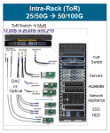
The modularity in hyperscale data center architectures is associated with the ubiquitous server rack, as depicted in the figure below.
Figure 1. Common server rack hardware configuration, illustrating optical module or Direct Attach Copper connectivity to the Top-of-Rack switch. (Source: Synopsys)
Top of Rack (ToR) is a common position for the network switch hardware. The figure above also indicates the increasing network switch bandwidth required – e.g., 25.6 Tb/sec and 51.2 Tb/sec – and the network interface card technologies used in these rack configurations.
When describing the connection bandwidth, the key parameters are:
- serial (SerDes) data rate and the number of SerDes lanes
The effective datarate is reduced (slightly) from the SerDes specification due to the additional bits added to the payload as part of the data encoding algorithm.
- insertion loss and crosstalk loss of the connection medium, and the range of the connection
The key overall specification to achieve is the bit error rate (BER), which is determined by a number of factors – e.g., Tx equalization, Rx adaptation to optimize signal sampling time, and especially, the frequency-dependent insertion loss and crosstalk interference of the connection.
For these very high-speed data rates, individual specifications for these losses are often provided (the loss acceptance mask versus frequency), for different configurations – e.g., chip-to-chip (short reach); backplane with 2 connectors (~1m), and Direct Attach Copper cable (~3m). Increasingly, above a 100 Gbps serial rate, copper cabling in the rack may be displaced by low-cost optics and/or a transition of the network switch to a middle-of-rack (“MoR”) position.
I had the opportunity to chat with Manmeet Walia, Senior Marketing Manager for High-Speed PHY Development at Synopsys, about the characteristics of the hyperscale data center, the increased data communications bandwidth, and the ramifications of these trends on hardware design.
“There are several key trends emerging.”, Manmeet indicated. “For improved efficiency, Smart network interface cards (“SmartNIC”) are being offered, with additional capabilities for network packet processing to off-load the host.”
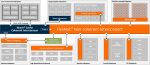
“The intra-rack bandwidth requirements are increasing – 56G and 112G Ethernet are required.”, Manmeet said. The figure below highlights how these IP are used in support of various aggregate Ethernet speeds, using multi-lane configurations. The targets for bandwidth between data centers are also shown below.
Figure 2. Evolution of Ethernet speeds, targets for DC-to-DC bandwidth. (Source: Synopsys)
“Switch designs are integrating electro-optical conversion and optical fiber connectivity for the Ethernet physical layer even in medium- and short-range configurations. Inter-rack and data center-to-data center bandwidth must also increase to accommodate the network traffic.”
Manmeet provided the figure below to illustrate how electro-optical conversion is transitioning from a distinct network card module to an integral part of advanced packages, with optical fiber used locally. (The electrical SerDes signal conditioning retiming functionality required at high data rates is thereby eliminated.)
Figure 3. Electro-optical conversion transition from a module to an integrated function. (Source: Synopsys)
He continued, “The 56G and 112G Ethernet communications requires PAM-4 signaling – conventional NRZ signal transitions for these networking applications maxes out at 28G.”
Figure 4. PAM-4 Signaling Eye Diagram and Test Challenges. (Source: Teledyne LeCroy)
Briefly, PAM-4 signaling implies there are 4 different possible voltage levels to be sensed at the center of the signal eye. The PAM-4 signal sensing window is therefore 1/3rd of the NRZ (PAM-2) height. The linearity of the 4 signal levels is a critical parameter.
As with an NRE serial signal, minimizing crosstalk noise is crucial, especially with the reduced voltage sense differences with PAM-4.
The time sampling in the center of the eye opening for the PAM-4 signal is more complex, as well. The jitter at the edges of the eye is magnified in PAM-4, due to the varying transitions between individual levels in successive unit intervals. Separate Tx and Rx clock sources are used for training and auto-negotiation, potentially on a per-lane basis. Additionally, there is a common requirement to support varying speed settings, again potentially for each lane.
The IEEE 802.3cd working group is establishing 56G/112G Tx/Rx signal specifications and PAM-4 standards for various network topologies, from ultra-short to long-reach, and for shielded/balanced copper and optical fiber cables.
“What’s new in the Synopsys PHY group?”, I asked.
Manmeet replied, “At the TSMC Open Innovation Platform symposium, we are highlighting our N7 56G and 112G PHY IP. We are also providing reference design evaluation hardware and software evaluation platforms for customers.”
Manmeet included the following roadmap for large network switch SoCs, integrating 256 lanes of the 56G and 112G PHY’s.
Figure 5. Example configuration of high-speed PHY’s, for large network switch SoC designs. (Source: Synopsys)
“The 56G PHY IP is provided in an X4 lane increment. The DesignWare Physical Coding Sublayer (PCS) enables the networking protocol to span a wide range of data rates. The 112G PHY is offered in an X1 lane unit, with similar PCS flexibility.”
Figure 6. Synopsys 56G and 112G Ethernet PHY implementation architecture. (Source: Synopsys)
Manmeet added, “Synopsys will be providing customers with additional design materials. SoC physical layout PHY tiling and power delivery recommendations are included, based on the results of our package escape studies. IBIS-AMI models are provided. A software toolkit enables evaluation of Tx and Rx settings and signal eye characteristics. A test chip evaluation card is also available.”
Figure 7. Design kit materials for 56G and 112G IP evaluation: IBIS-AMI model, software toolkit for lab evaluation, reference card. (Source: Synopsys)
Several trends are clear:
- Computing models are rapidly adopting the characteristics of flexible “hyperscale” data centers.
- The volume of network traffic demands an increase in bandwidth to 400G, enabled by the availability of 56G and 112G Ethernet PHY IP utilizing PAM-4 signaling, whether for short-reach or long-reach configurations, utilizing copper or optical cable physical layer interconnects. (For ultra-short reach interfaces, these Synopsys PHYs also include options to optimize power for low-loss channels.)
- The complexities of integrating a large number of high-speed 56G/112G Ethernet PAM-4 SerDes lanes to optimize signal losses and crosstalk requires more than just “silicon-proven” test chips from the IP provider. A strong collaboration between customers and the IP provider is needed to adapt to the SoC metallization stack and to leverage the available software/hardware reference materials.
Here are links to additional information that may be of interest.
Synopsys 112G Ethernet PHY IP press release – link.
Article: “Shift from NRZ to PAM-4 Signaling for 400G Ethernet” – link.
Youtube video on 7nm 56G Ethernet PHY IP performance results – link.
Synopsys DesignWare 112G Ethernet PHY IP – link.
-chipguy