Semiconductor industry evolution was largely a U.S. phenomenon. While there were important contributions made by persons all over the world, the basic technology grew from the invention of the transistor at Bell Labs which was licensed broadly in the U.S. That created a level playing field for all who wanted to become producers. The industry then evolved in a free market environment in the U.S. largely without regulation or patent disputes. By 1965, three companies, TI, Motorola and Fairchild, had a combined market share greater than two thirds of worldwide sales of semiconductors (Figure 7, Chapter Five). Barriers to the internationalization of the industry emerged through import tariffs in Europe and restrictions on setting up subsidiaries in Japan but even these limitations gradually disappeared.
After 1965, the semiconductor industry began a near continuous deconsolidation as new companies entered the market. The market share of the largest competitor remained about the same for the next fifty-five years at 12 to 15% (Figures 7 and 8 in Chapter Five). Top ten semiconductor companies during the 1950s and 1960s did not include any non-U.S. companies (Figure 10, Chapter Five).
Japan Becomes a Significant Competitor
In the late 1970s and early 1980s, the industry became international with the entry of NEC, Toshiba, Hitachi and Matsushita into the list of the top 10 largest semiconductor companies. Philips, a European semiconductor company, also entered the top ten for the first time. The Japanese phenomenon was driven largely by the superior manufacturing process control applied to dynamic RAMs, or DRAMs. This was the first wave of “trade wars”. The Japanese Ministry of Industry and Trade, MITI, coordinated actions among Japanese companies that contributed to a cooling of tensions between SIA (U.S. Semiconductor Industry Association) and EIAJ (Electronics Industry Association of Japan). Japanese companies were assigned quotas for purchases of semiconductors from U.S. companies, relieving some of the pressure. The real end to the issue was predictable but not so obvious to many of us. At a dinner I had with Saturo Ito, CEO of Hitachi Semiconductor, in the late 1980s, he explained to me that the U.S. shouldn’t worry about Japan taking over most of the manufacturing of semiconductors in the world, as I had feared. Ito told me, “Japanese are optimizers, not inventors. When standards are stable, Japan will do well. When standards are evolving, not so well.” He was right. As the personal computer and cell phone industries grew, the U.S. recaptured substantial innovation momentum.
Enter Korea
Less predictable than the Japanese success in DRAM manufacturing was the entry of Korea. When Samsung announced its intent to design and produce the 64K DRAM and sent their managers on a 64-mile hike as a symbolic start, we didn’t pay much attention. How could they catch up in an industry that was so mature?
Their success came from the determination of Koreans when they decide upon a specific goal. The path was not easy. As late as 2008, the combined market share of the three largest DRAM producers in the world, Samsung, SK Hynix and Micron, was only modestly greater than 50% of the entire worldwide market. Today, their combined market share is greater than 95% (Figure 6 of Chapter Five).
Taiwan
As with Japan, Korea and China, Asian governments understood very early the importance of domestic semiconductor capability. Evolution of worldwide leadership in the silicon foundry business by Taiwan is truly remarkable. The Taiwanese semiconductor industry grew from a team of Taiwanese engineers who went to work for RCA in the late 1970s. These individuals were very talented. They started many semiconductor companies when they returned to Taiwan. When the Taiwanese government formed ITRI and ERSO to promote advanced development in Taiwan, the country was fortunate to have Morris Chang, former head of TI’s semiconductor business, available to move to Taiwan to head up these two entities. When TSMC and UMC were formed, Morris filled the role of Chairman of both. Securing funding from Philips, he was able to take advantage of an unlikely transition of the semiconductor industry. Those of us in the industry at the time wondered how a company whose business consisted only of wafer fabrication could ever survive. Those of us working for integrated device manufacturers like TI viewed wafer fabs as our biggest problem. Whenever a recession came along, the fabs became under-loaded and were astoundingly unprofitable. The depreciation cost continued but the revenue did not. If someone else was willing to take over the wafer fabs, then the semiconductor business volatility would be reduced making it a more attractive, stable industry. The U.S. had already experienced the pain of wafer fab ownership when Japanese competitors in the 1985 recession kept running wafers at a loss, partly because they couldn’t lay off their people. In the U.S. we shut down some of our wafer fabs to stop the financial bleeding. Step by step we created an opportunity for Japan to gain market share when the recovery inevitably came. Now TSMC and UMC in Taiwan were taking over the one aspect of the industry that caused us the greatest pain.
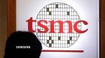
TSMC recognized the value of being a dedicated foundry with no products of its own to compete with its customers, unlike its competitors such as UMC, Seiko Epson, NEC and more. By becoming a pure play foundry and popularizing its design rules, TSMC gained momentum that was hard to match. Today, only Samsung comes close to providing real competition at the leading edge of semiconductor technology.
This leaves the U.S. in the interesting position that, other than Intel plus some limited capacity in Texas and New York, there is no significant domestic manufacturing capability at the advanced nodes of semiconductor technology. Anything that disrupts free trade between Taiwan and the U.S. could severely disrupt much of the U.S. manufacturing and defense industries.
China
Despite China’s rise as the world’s largest assembler of consumer electronic equipment, the Chinese semiconductor industry has evolved slowly. The largest Chinese semiconductor foundry, SMIC, is still two technology nodes behind TSMC in manufacturing capability as of 2019.
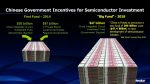
The Chinese government is dedicated to changing this situation. Figure 1 shows the investment that is being made.
Figure 1. Chinese government stimulus for semiconductor investment has been matched by a much greater investment by private equity companies
These numbers dwarf anything that the U.S. government is likely to do. The entire annual revenue of the worldwide semiconductor industry is less than $500 billion. The Chinese government is investing more than $20 billion per year. They are doing it in an insightful way. The money is invested as a share of private equity companies who are motivated to invest in semiconductor companies that can make an attractive return on the investment. Many of the startup companies have an optimistic outlook because the Chinese population of over one billion people can drive its own standards for communications and computing.
How well have they done with the investment? Figure 2 shows a comparison of the size of the semiconductor companies that have benefited from the investment.
Figure 2. Growth of Chinese fabless semiconductor companies
Average employment of the semiconductor companies in China has grown between 2006 and 2015. The number of companies with more than five hundred employees in 2006 was less than one half of one percent. In 2015, it was 6.1%. The number of Chinese fabless semiconductor companies that had between 100 and 500 employees in 2006 was 9.8%. In 2015, it was 43.3%. This growth provides a challenge for semiconductor competitors in the rest of the world including the U.S. where governments can’t afford to provide the kind of subsidies that are available in China. Even so, the problem was manageable with innovative U.S. companies operating in a semi-free market environment for creating new technologies. The U.S., however, created a “Sputnik moment” for China that may have changed the outlook.
Historical Perspective of Export Controls
In 1982, I joined the Technical Advisory Committee of the Department of Commerce that was set up to advise the Department regarding the granting of validated licenses for export of semiconductors and semiconductor manufacturing equipment. Soon I became Chairman of the committee. In the 1970s, U.S. companies like Applied Materials, Lam Research, Novellus, Varian and many more dominated the worldwide semiconductor manufacturing equipment business. Japanese companies like TEL were growing but their base of customers was largely in Japan. The Export Administration Act of 1979 was one of the contributing factors that changed that competitive situation. Concern about the military implications of semiconductor capability led to a set of restrictions on semiconductor related exports from the U.S. and its allies to controlled destinations that were enemies of the free world.
Allies like Japan were much more efficient at administration of bureaucratic export control rules. Validated licenses for customers of Japanese manufacturers could reliably be obtained in three days plus or minus a day or two. For the U.S., the time and the variability were much greater. Companies in places like Taiwan rightly concluded that the U.S. could not be trusted as a supplier because spare parts and user manuals also required separate validated licenses. Market share of U.S. companies in the semiconductor manufacturing equipment industry fell from more than 4X Japan’s market share in 1980 to about equal shares for Japan and the U.S. in 1990. In a sense, the U.S. moved toward a role as the “vendor of last resort” for semiconductor manufacturing equipment sold to controlled destinations and probably even to some destinations that were COCOM allies.
China’s Sputnik Moment
ZTE clearly violated internationally accepted export restrictions on Iran. The U.S. reaction was not totally unexpected. What surprised the world was the swift action taken to shut down the free market purchase of semiconductor components. The degree of dependence that ZTE had developed upon U.S. semiconductor suppliers made this a life or death issue for the company. President Trump ultimately waived the export restrictions. Although the embargo was lifted, the impact of the threat was now apparent to China. Dependence upon U.S. suppliers of semiconductors was no longer a viable strategy.
As the Chinese government continued its move toward dictatorship, rules were imposed upon foreign companies for the opportunity to establish operations in China. Google was prevented from operating in China, as were others. These restrictions became increasingly egregious (such as the threat that U.S. software companies might have to turn over their source code to the Chinese government if they wished to operate in China). As frictions developed in the trade negotiations between the U.S. and China, a U.S. decision was made to embargo exports to Huawei by placing Huawei on the “entity list”. This created an even more untenable situation for China, the worldwide leader in wireless communication technology.
China did the expected. They focused upon developing non-U.S. capabilities for all their components. Since China buys more than 50% of all semiconductor components in the world, this is a big problem for the U.S. semiconductor industry. It is probably not reversible.
Another question is whether other countries will follow suit out of fear that political disagreements with the U.S. could result in an embargo of semiconductor components from U.S. suppliers. As with the Export Administration Act, events in China will lead to a reduction in market share of U.S. based semiconductor suppliers and a loss of their lead in many new technologies.
How long will it take for China to eliminate its dependence upon U.S. semiconductor suppliers? Probably many years, especially for FPGAs and RF components, and it may never be achieved. China’s demand is so large that non-U.S. suppliers will probably find a way, given enough time, to displace U.S. suppliers but it’s hard for any country to become totally self-sufficient. In addition, China’s move toward a closed, controlled society will restrict innovation. That will work to the advantage of the U.S.
While China’s direction is not likely to change, we still have the possibility of convincing the rest of the world that the U.S. can be treated as a reliable supplier. Hopefully, there will be policies articulated by the U.S. that convey that confidence and restore the U.S. position as a leader in free trade.


