

On Monday, July 8th Imec held a technology forum ahead of Semicon West. I saw the papers presented and interviewed three of the authors. The following is a summary of what I feel are the keys points of their research.
Arnaud Furnemont
Arnaud Furnemont’s talk was titled “From Technology Scaling to System Optimization”. Simple 2D dimensional scaling has slowed. Design Technology Co-optimization (DTCO) has led to track height reduction but as track heights shrink it leads to fin depopulation and requires process optimization to maintain performance. DTCO and scaling continues to be important, but we need to also look from the top down as scaling from a system perspective using System Technology Co-Optimization (STCO).
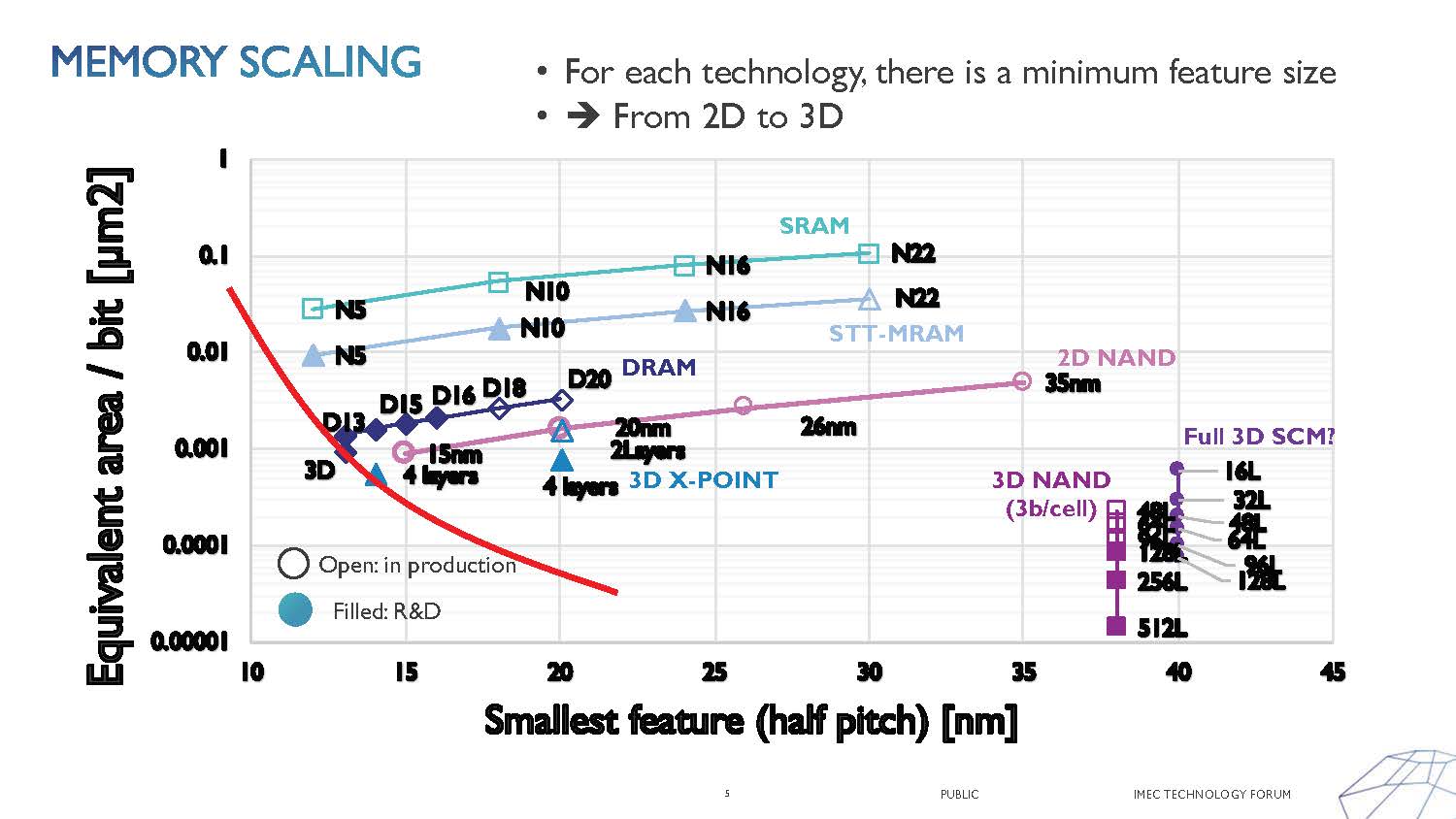
As dimensions scale down a limit is eventually reached for each technology and a transitions from 2D to 3D is required. We have already seen this happen with 2D NAND transition to 3D NAND. For DRAM’s he sin’t convinced capacitor scaling continue below the D13/D14 nodes and a 3D solution is needed. 3D XPoint memory will need to increase the number of layers and logic will also have to transition to 3D.
Figure 1 summarizes half pitch limits for memory by technology.

Figure 1. Memory Scaling Limits.
For logic scaling there are opportunities to partition functions in an intelligent manner. Backside power delivery through thinned wafers with micro TSVs and separately fabricating SRAM and logic and then integrating them offer options for more highly optimized solutions, see figure 2.

Figure 2. Smart Partitioning.
I have previously written about backside power delivery here.
Naoto Horiguchi
Naoto Horiguchi gave a paper entitled “Vertical Device Options for CMOS Scaling”. The main point of the papers was that vertical devices could provide a shrink to SRAM arrays versus horizontal tarnsistors, see figure 3.

Figure 3. SRAM Shrink from Vertical Transistors.
This work fits in with the previous paper because by fabrication an SRAM only array the process scan be simplified versus a full logic process, for example SRAM only requires approximately 4 interconnect layers versus 12 or more for leading edge logic.
Figures 4 and 5 illustrates the basic process for a 5nm class vertical SRAM array. The process steps in blue are EUV layers (note that the Top Electrode is mot in blue but is also an EUV layer).

Figure 4. Vertical SRAM Array Front End Of Line (FEOL) Process.

Figure 5. Vertical SRAM Array Back End Of Line (BEOL) Process.
This work was also published at the VLSI Technology Forum [1] and between figures 4 and 5 and the VLSI paper the process becomes the process can be outlined in more detail.
- An N-type Epi layer is deposited.
- 2 noncritical masks and implants are used to fabricate high doped N and P wells.
- A 70nm thick P-type channel Epi layer is grown.
- An EUV mask and etch is used to form 8nm diameter nanowire pillars. The etch is 100nm deep etching down into the high doped wells.
- An EUV mask and etch is used to create isolating trenches between sets of pillars.
- The trench is filled and then an oxide recess etch is performed, this exposes the upper areas of the pillars for gate formation.
- A chemical oxidation is performed to create and interface oxide, this is followed by ALD depositions of HfO2 and TiN.
- A Tungsten (W) fill is now deposited, CMP planarized and then a recess etch is performed.
- An EUV mask and etch is performed to form the gates and then an oxide fill is performed.
- An EUV mask, etch and W fill is performed to create the bottom gate contact.
- An EUV mask, etch and W fill is performed to create cross couples.
- A barrier layer is deposited, masked and etched and then a selective epi of Si:B is grown to form the top source/drain for the PMOS.
- A barrier layer is deposited, masked and etched and then a selective epi of Si:P is grown to form the top source/drain for the NMOS. An oxide is then deposited.
- An EUV mask, etch and W fill is performed to create the top electrode. An ILD oxide layer is deposited and planarized.
- An EUV mask, etch and W fill is performed to create the gate contact.
- An EUV mask, etch and W fill is performed to create the top electrode contact.
- An oxide is deposited and planarized, an EUV mask and etch is used to create a metal 1 trench that is then filled with damascene copper.
- An EUV mask, etch and W fill is used to create a super via.
- EUV masks and etches are used to create metal 2 and via 2 and then they are filled with dual damascene copper.
This flow is used to create Vertical SRAM test devices. A full flow would include at least two more metal layers and likely some processing for ESD protection. This array could them be integrated with logic and backside power distribution as shown in figure 2.
Zsolt Tokei
Zsolt Tokei presented a paper entitle 3nm Interconnects and Beyond: A toolbox to Extend Interconnect Scaling”. In order to continue to scale down interconnect issue with resistance-capacitance (RC), cost, variability and mechanical stability need to be addressed. Figure 6 summarizes the path forward.
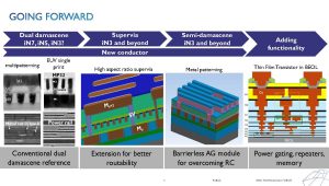
Figure 6. The Path Forward.
Conventional dual damascene and super vias for better routing give way to barrierless interconnect with air gaps possibly fabricated by semi-damscene. There is also research into integrated thin film transistor into the BEOL for increased functionality.
The semi-damascene is as follows:
- A via opening is patterned and etched in a dielectric film.
- The via is filled with Ruthenium (Ru) and Ru deposition continues until a layer of Ru is formed over the dielectric.
- The Ru is then masked and etched into metal lines.
- Air gaps are formed between the metal lines.
The Ru has a Titanium (adhesion layer) but the via to metal line interface is continuous Ru reducing resistance and the air gaps reduce the capacitance. Zsolt wouldn’t discuss the air gap formation process but presumably some kind of conformal film is deposited and then pinched off with another deposition.
This technique was used ot fabricate the world’s first 21nm pitch interconnects. Figure 7 summarizes the results.

Figure 7. 21nm Pitch Interconnect.
Figure 8 illustrates a thin film transistor (TFT) in the BEOL and describes some applications.

Figure 8. BEOL Thin Film Transistor.
Conclusion
Imec continues to produce cutting edge research to support continued scaling and improvements in semiconductor performance.
[1] M.-S. Kim, N. Harada, Y. Kikuchi, J. Boemmels, J. Mitard, T. Huynh-Bao, P. Matagne, Z. Ta1, , W. Li,
K. Devriendt, L.-A. Ragnarsson, C. Lorant, F. Sebaai, C. Porret, E. Rosseel, A. Dangol, D. Batuk,
G. Martinez-Alanis, J. Geypen, N. Jourda1, A. Sepulveda, H. Puliyalil, G. Jamieson, M. van der Veen, L. Teugels, Z. El-Mekki, E. Altamirano-Sanchez, Y. Li2, H.Nakamura, D. Mocuta, F. Masuoka, “12-EUV Layer Surrounding Gate Transistor (SGT) for Vertical 6-T SRAM: 5-nm-class Technology for Ultra-Density Logic Devices,” VLSIT Symposium (2019).


Consolidation and Competition: Who is Winning the $4.5 Billion Interface IP Race?