
I recently wrote about Tensilica’s HiFi DSPs which played a significant role at Cadence’s Automotive Design Summit which was held on the Cadence San Jose campus at the end of July. That article focused on infotainment while briefly touching on Advanced Driver-Assistance Systems (ADAS). ADAS is NOT synonymous with autopilot. Level 2 automotive ADAS features help the driver to drive more safely and also complement additional ADAS safety features in the current fleets of deployed cars, buses, trucks. The technologies used in ADAS are merely one step along the way to driverless or full self-driving (FSD) vehicles if viewed as a continuum. We define the progression to driverless or FSD vehicles like this:
Level 0: No automation
Level 1: Driver assistance
Level 2: Partial automation
Level 3: Conditional automation
Level 4: High automation
Level 5: Full automation
The most advanced ADAS features available in production cars today are Level 2/3. There are some limited taxi-like early pilot test services available now with Level 4 with limited range and use-case testing, subject to NHTSA guidelines. Cadence is doing a great job of making the EDA tools and IP available to build and enable these types of safe vehicles. But before we get into those details, I wanted to point out two important statements that stuck in my mind from the event: (1) security is more important than safety; and (2) several legal issues regarding autonomous vehicles have yet to be addressed.
The explanation for the higher priority security over safety is simple. If someone with evil thoughts can take over control of your vehicle, you are no longer safe. If someone else has control of your vehicle, they can determine where it goes, or they can crash it. Or they can be very annoying and blast music at full volume while leaving your wipers running continuously. If they can control one car, why not millions all at once? Unsecure autonomous driving systems would be unsafe and likely deadly. We must put security first, though safety is also critical. The crucial requirement of security is why Cadence’s relationship with Green Hills is so important. It will take software and hardware working together to implement the needed levels of security in autonomous FSD vehicles.
Autonomous vehicles are expected to reduce traffic fatalities dramatically. However, not all fatalities will be avoided. According to the World Health Organization (WHO), there were 1.25 million road traffic deaths globally in 2013. I think it would be fantastic if by 2032, through the increasing use of autonomous vehicles, we can cut that number in half. But that still means there would be over 600,000 traffic fatalities. Would we blame the car manufacturers? Would they be sued over every collision? Let’s face it, even if they reduce the number of traffic fatalities by 90%, when people get injured, they still want to blame someone. How will this work?
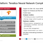
Sorry for the detour, but these things are important. Tensilica is enabling the drive from Level 2 ADAS up to Level 5 FSD by supplying a crucial piece of the autonomous driving system IP, artificial intelligence (AI). The Tensilica DNA 100 processor IP can handle the demands of the latest features in ADAS such as neural networks based emotions and Facial Action Coding Systems (FACS), gesture tracking, and occlusion detection. The number of new AI features in the pipeline for our cars is staggering. Beyond all that, the Level 5 systems will have many AI processes monitoring a huge hub of sensors and communication networks/protocols while also providing navigation, mapping, and trajectory planning with a focus on safety. AI neural networks will be key to all of this, and Tensilica will be a key IP supplier of AI-based systems.
I came away from the Cadence Automotive Summit impressed with Cadence’s overall grasp of the needs of the designers of autonomous driving systems. They seemed to have expertise in every field, and partners where the required expertise is well outside the Cadence domain. My thanks to Pradeep Bardia, Cadence Product Marketing Group Director for AI, for his presentation on “Automotive – AI Processor Solutions.” And thanks also to Robert Schweiger, Cadence’s Director of Automotive Solutions, for the timely and insightful event.


