webinar banner2025 (1)

Magillem offers a practical UPF power flow

Magillem offers a practical UPF power flow
by Tom Simon on 05-28-2019 at 10:00 am

We already know that IP-Xact is extremely useful for managing IP and SOC design specifications, yet it may come as a surprise to learn that it also can be used to form the basis of a power flow too. There are design tools that read UPF to help implement and verify designs, however it can be extremely useful to understand the interplay between the power intent and the fully elaborated design early in the flow.

First off, let’s back up and talk about how designs with multiple power and voltage domains are specified. In theory, and often in practice, the RTL for a design provides no guidance for power domains or voltage domains. Of course, there may be a mode controller in the RTL, or the design might be completely power agnostic. Certainly, the RTL will not have information about signal levels between blocks or information about implementation of the power nets. This is where UPF comes in.

UPF works in conjunction with the RTL to fully define the details of the supply connections and the signals that cross domains. Power and ground nets may be connected or disconnected to save power in certain operating modes. Signals may need level shifting, and isolation or retention when blocks switch off. UPF is based on the logical hierarchy, which is available in a fully elaborated design.

Magillem’s IP-XACT Power FLow

Writing UPF directly can be a daunting task. Magillem, a leading provider of IP-XACT solutions, saw a way that IP-XACT and power intent can be combined to make specification of power intent easier, and used to check for issues before moving into the implementation phase. IP-XACT already provides a way to create, manage and elaborate an RTL design, by capturing information for the hierarchy, block interfaces, buses and signals. Magillem realized that tabular input through csv files is an ideal way to specify power domains, voltage domains, power states, isolation rules and level shifter rules. These can be applied to the fully elaborated design to create a complete specification.

Using this flow mismatches between the power intent and the design can be easily detected. Magillem has also implemented checkers for missing level and isolation elements. Propagated power properties are reported, as well as any warning or errors. Their IP-XACT power flow provides verbose reports to provide easy traceability. Magillem’s power flow outputs a domain based virtual hierarchy and offers visualization so that it is easy to understand the domain partitioning. Then in the final step it outputs UPF 2.0 for use downstream in the design flow.

Mistakes in specifying power intent can be fatal and navigating through reams of UPF looking for issues can be frustrating. Magillem makes the entire process easier by letting the designer work on the fully elaborated design and get a clear picture of what domain each instance is in. Magillem’s power flow can ensure that there are no missing level shifters. It also can help ensure that level shifters, isolation and retention are in all the necessary locations. While UPF provides a nice partitioning between design and power specification, it’s good to know that Magillem’s power flow offers a high-level solution for integrating and verifying them early in the design process.


JasperGold Gets Smarter, Faster and Easier for Signoff

JasperGold Gets Smarter, Faster and Easier for Signoff
by Bernard Murphy on 05-28-2019 at 5:00 am

Machine learning (ML) is already making its way into EDA tools and flows, but the majority of announcements have been around implementation, especially in guiding toward improved timing and area. This is a pretty obvious place to start; ML is in one sense an optimization technique, trained on prior examples, which should be able to provide further PPA optimization over traditional methods. Conversely, few announcements have been made about ML applications for (functional) verification, perhaps because incremental optimization angles for verification aren’t quite so self-evident, beyond general assertions that “something” ought to be possible. I don’t doubt this situation will change; creative verification tool/flow makers will find ways to apply ML in ways that aren’t so obvious.

That this is already possible is clear in advances Cadence have made in their new, smart JasperGold Formal Verification Platform. I suspect progress started here first because formal platforms have some things in common with implementation platforms – multiple engines to accomplish a goal in different ways and lots of knobs to control how those engines work. The JasperGold Smart Proof technology exploits these two factors directly. For optimization within an engine (Anirudh calls this ML-inside), the tool provides training data built on 500+ customer designs to parameterize that solver for optimum performance.

There’s also an important optimization in solving across engines. It is common in formal verification to use more than one engine to attempt a problem since engines have different strengths playing to different classes of problem. You could first try one approach and if that doesn’t succeed after some number of cycles, switch to a different approach. But that’s old-school. A newer approach depends on orchestration – a semi-automated method to launch multiple runs, each with a different strategy – to find a best-case outcome as quickly as possible. ML-based orchestration takes this one step further, learning again from runs on those 500+ test cases, how best to optimize that orchestration (Anirudh calls this ML-outside). Orchestration starts with out-of-the-box supervised learning, giving you value from day 1 then adding on-going proof-profiling based on your usage to further improve performance.

What different does this make? Pete Hardee (Dir Product Management at Cadence) tells me that across a representative set of designs, they are seeing ~10X faster properties proven per second, and on a set of known “hard” designs in which it is difficult to get to proofs on many properties, they were able to reduce inconclusive proofs from 46% to 29%.

When you’re king of the hill, you don’t want to rest on just one advance. Pete tells me this new release also compiles 2X faster and in a 2X smaller memory footprint. This has been measured on multiple designs, up to 100M+ gates. Now wait a minute – this is formal, the technology that only works with small designs, right? Pete told me that yes, you’re ultimately going to want to abstract or otherwise reduce to get to a manageable problem for proving, but why force you to do that before you even readin the design? All those steps, including useful analysis (like cone-of-influence) can be done on the build image and you can let the tool take care of the heavy lifting in applying abstraction, etc.

Last and certainly not least, they have put significant work in integrating and simplifying the analysis GUI with aim to support signoff-quality coverage. I’ve talked before how you can integrate formal coverage with dynamic coverage through vManager. They’ve added an all-new coverage analysis GUI in support of the formal side of this, tracking coverage runs versus proof runs, providing easily accessible information on dead-code and over-constraints, a unified view of proof-core and cone-of-influence coverage and a new formal coverage metric looking at both stimuli and checkers.

Not only is Cadence a clear leader in formal, it looks like they’re working hard to stay there. Check out the new updates HERE.


56th DAC Empyrean Stepping Up ALPS with GPU Implementation

56th DAC Empyrean Stepping Up ALPS with GPU Implementation
by Daniel Nenni on 05-27-2019 at 11:00 am

As a testament to the technology advances developed and implemented into Empyrean ALPS™ by the engineering team, the product has seen a steady growth in the adoption by users. In addition, hearing directly from the users at DAC 2018 turned out to be an all-around success for the product as well as the product team to see ALPS beating other established parallel SPICE simulators in performance while maintaining the same accuracy. When good work is recognized, engineering motivation shoots up and greater outcomes begin to happen. You can see that in the form of GPU-accelerated ALPS at the 56th DAC. The recent announcement of Empyrean ALPS being voted by users at DAC 2018 as “Best of 2018 DAC” in SPICE simulation is yet another recognition of the product and the product team. The outcome of all the above is the introduction of a GPU-accelerated ALPS at the upcoming 56th DAC at Las Vegas, Nevada.

SPICE Simulation Challenges

In any typical SPICE simulation run, close to 90% of the time is spent on two operations: Device model evaluation and matrix solving. Empyrean’s engineering team came up with a novel algorithm, the Smart Matrix Solver (SMS) to address matrix solving. A multi-threaded, CPU-based architecture and the Smart Matrix Solver empowered ALPS to run not only faster, but also maintain the same accuracy with SPICE. The speedups were to the tune of 3X to 8X over other simulators and without the need for accuracy trade-off using model simplification of RC reduction techniques on analog and mixed-signal designs, especially with post-layout simulations runs where the parasitics add up to tens of millions of elements, impacting performance and accuracy. Click here for user feedback on ALPS. Join us at the 56th DAC in Las Vegas, Nevada at the Empyrean booth #651 to learn about Empyrean ALPS.

Stepping Up with GPU-Based Architecture

The product success further motivated the engineering team at Empyrean which had been actively working on a GPU-based implementation. With a GPU-based architecture, they were able to cleverly direct and massively parallelize the two time-consuming operations, device model evaluation and matrix solving to the GPUs with 1000s of cores, while keeping rest of the simulation operations on the CPU. Working closely with some key customers, the most common hardware, NVIDIA’s Tesla V100 was selected as the platform to use. NVIDIA’s CUDA™ solver that came with V100 was fast but not fast enough for SPICE runs. The team enhanced the Smart Matrix Solver by optimizing it for GPUs to achieve greater simulation performance while keeping accuracy. Empyrean will be talking to early customers for this product, called Empyrean ALPS-GT™ at the suite at DAC.

AI -Powered IP Timing Arc Prediction

Further strengthening its position in the AMS design, Empyrean will be showcasing a new AI -powered timing arc prediction especially for analog and mixed signal IP and library circuits. This is a capability that Empyrean developed by working closely with a few key customers. A joint paper with NVIDIA is being presented on this at the Designer Track session at DAC 56 (Paper ID:268-WC54).

Timing arc prediction for an analog or AMS circuit is relatively difficult, and with the AMS content continuously increasing in SoCs, the need for accurate prediction is critically important and can often lead to costly silicon failures. Please stop by the Empyrean booth (#651) to learn about this capability in Empyrean Qualib-AI™ product and how it is being applied to designs.

The most recent blog on SemiWiki by Daniel Payne goes into more details on the GPU-accelerated SPICE and the AI-powered Qualib.

Better SoC Design, Debug and Analysis

Empyrean’s claim to fame in the SoC market was with Empyrean X-Top™, a comprehensive timing eco analysis and fixing capability, which was first adopted by Marvell, and later making it a required sign-off tool in their flow. X-Top is an ultra large capacity placement and routing aware timing eco engine with automated and interactive eco capabilities. Today’s complex multi-voltage domain designs with simultaneous multi-mode multi-corner (MMMC) optimization are ideal candidates for this tool. Stop by Empyrean’s booth at DAC to check out X-Top and how it is in the tape-out flow of many companies.

Empyrean’s ClockExplorer™ is another valuable solution for diagnosis and analysis of clock circuits in today’s designs with complex clock domains. Its powerful visual diagnosis capabilities provide the back-end implementation teams the ability to easily visualize clock networks and implement it as intended by the front-end design team, thereby reducing unnecessary silicon iterations. Stop by the Empyrean booth to check out ClockExplorer.

Skipper™ has been a great add-on to the SoC design flow at many companies to analyze very large pre and post-silicon layout database for anything from DRC/LVS debug to failure analysis. Its very fast layout bring-up, IP merging and post-silicon FIB processing along with powerful diagnosis and analysis capabilities make it an attractive add-on to many SoC design flows. Skipper was also recognized by users at DAC 2018 as “Best of 2018 DAC.” Click here for the user feedback on Skipper. Stop by the Empyrean booth to check out Skipper.

About Empyrean Software

Founded in 2009, Empyrean Software is an Electronic Design Automation (EDA) and intellectual property (IP) technology leader in delivering fast and true physically aware, design closure and optimization solutions for timing, clock and power of system on chip (SoCs). The company also offers a high-performance accurate circuit simulator and is an analog IP and fast SerDes IP provider. For details, go to Empyrean Software.


The Changing Landscape for SPICE Circuit Simulators

The Changing Landscape for SPICE Circuit Simulators
by Daniel Payne on 05-27-2019 at 5:00 am

Empyrean - ALPS

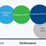
I first started using a SPICE circuit simulator in 1978 while at Intel and have followed that market ever since then. Back at DAC in 2012 I first heard of a Chinese EDA company called IC Scape with a SPICE circuit simulator called Aeolus, so I blogged about it. Fast forward to 2019 and I heard from Ravi Ravikumar, a former co-worker from Viewlogic days in the 1990s and he was excited to talk about Empyrean, because they have the tools from IC Scape plus they’ve added even more EDA tools. You’ve probably heard of classic SPICE and the more modern Fast SPICE simulators, so the following chart shows where the Empyrean simulators fit into that space:

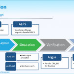
The ALPS acronym stands for: Accurate, Large capacity, Parallel, SPICE. The GT suffix stands for: GPU-Turbo. Other companies and Universities have attempted to use a GPU to speed up the matrix math used in SPICE, but none of them have had commercial success, until now. So, why would you employ a GPU for SPICE circuit simulation?

  • 10X faster simulation speeds versus using a 16-core simulation
  • 7nm IC designs have massive SPICE requirements

Empyrean ALPS-GT runs on the Nvidia Tesla V100, and it simply outperforms SPICE simulator running on an Intel Xeon 8180, for example. OK, that sounds attractive, but as an engineer I want to know how it operates under the hood. The matrix math library found in the CUDA library could be used for SPICE, but it’s not fast enough or efficient enough, so the team at Empyrean wrote their own matrix solver to run on the Nvidia GPU.

Comparing the Nvidia Tesla V100 versus an Intel Xeon 8180:

  • Cores
    • Xeon 8180: 28 physical cores
    • Tesla V100: 5,276 FP64 cores
  • Double precision floating-point performance (FP64)
    • Xeon 8180: 2T flops
    • Tesla V100: 7T flops

In benchmarks between the Nvidia CUDA matrix solver versus the Smart Matrix Solver from Empyrean, the new approach is 5.8X faster on average. Comparing a CPU with 16 cores versus 8 GPUs, the ALPS-GT simulator was 6.4 to 16.9X faster. So that’s how you make your GPU-based SPICE simulator faster than the competition, impressive.

DAC Designer Track

I hope that you can make it to DAC56 in Las Vegas, but if not I wanted to at least tell you something about a paper authored by Empyrean (An-Jui Shey, Jason Xing) and Nvidia (Eric Hsu, Ting Ku):

Qualib AI: Machine Learning Based Arc Prediction of Timing Model for AMS Design

For AMS timing models you can use the manual method of defining timing arcs, which is time consuming and error prone, or you can apply machine learning to find more timing arcs. Empyrean has a commercial tool called Qualib that is a library/IP QA and debugging platform, but the paper shows how they have extended that for Nvidia to make Qualib AI, which is not commercially available yet, so stay tuned.

Let me show you a couple of diagrams, the first one is an application flow for timing arc prediction, the second one is timing arc modeling and prediction algorithm:

Timing Arc Prediction
Timing Arc Modeling and Prediction Algorithm

What Nvidia found in using Qualib AI is that the tool:

  • Found a significant number of real, missing arcs in live projects
  • Reduced the number of false positive missing arcs
  • Runtime allowed interactive prediction
  • Using increment training for better accuracy
  • Predicted timing types

Summary

The team at Empyrean has been busy creating a GPU-based SPICE circuit simulator and applying AI to complex IP blocks in order to shorten development times at Nvidia. They are certainly on my radar to keep a watch on, because if they can satisfy the leading-edge demands at Nvidia then they are definitely a contender for new EDA tool evaluations. Why use old technology, when something newer comes along?


Semiconductor IP Security Issues

Semiconductor IP Security Issues
by Daniel Payne on 05-26-2019 at 4:46 pm

Accellera

Every morning I read the headlines from SemiWiki, CNN, LinkedIn and my Twitter feed, and it seems like every week that I read about another security breach that makes me wonder if anything online is secure. Companies try to harden their web sites, IT infrastructure and even their electronic products from being exploited or tampered with. Every article that you read about the IoT and connected devices is sure to mention security. Now let’s take the next step and say that you are designing a new SoC and intend to use hundreds of IP blocks, many from 3rd party vendors, so how do you know that each IP block will function properly and securely once integrated into a system?

I know that in the software world that we get new updates to improve the security of so many things, like: Operating Systems, desktop apps, mobile apps. Even my bike computer and cycling power meter have updates to fix bugs and make them more secure. Every semiconductor IP company has a process for making each IP block secure, but what about the entire industry?

Thankfully our industry has a well-known standards body, Accellera, and they have recently formed an IP Security Assurance Working Group.

Brent Sherman from Intel is the Chair, along with Mike Borza from Synopsys as the Vice Chair, so this looks like a solid start to tackle this concept of IP security across our semiconductor industry. You may even want to join this working group, so begin the process.

DAC 56 is coming up in June, so you should consider attending a luncheon and panel discussion on this timely topic of IP security assurance. The event is planned for Monday, June 3rd from Noon to 1:30PM in Room N246 in the Las Vegas Convention Center. It’s easy to register online here.

Accellera Chair Lu Dai will kick off the panel, and it should be lively and informative. The following speakers are panelists:

Brent Sherman, Intel
Lei Poo, Analog Devices
Serge Leef, DARPA
Andrew Dauman, Tortuga Logic
Adam Sherer, Cadence

I’ve worked at companies with both Serge Leef and Andrew Dauman, so these panelists are smart, experienced and articulate on the topic of IP security.

Summary

Exploitable vulnerabilities can be mitigated in semiconductor IP, so Accellera is forging ahead with an IP Security Assurance Working Group to create a standard that our industry can define and follow. Visit their web site and plan to attend the DAC luncheon and panel discussion to learn and participate.

Accellera

Accellera Systems Initiative is an independent, not-for profit organization dedicated to create, support, promote, and advance system-level design, modeling, and verification standards for use by the worldwide electronics industry. We are composed of a broad range of members that fully support the work of our technical committee to develop technology standards that are balanced, open, and benefit the worldwide electronics industry. Leading companies and semiconductor manufacturers around the world are using our electronic design automation (EDA) and intellectual property (IP) standards in a wide range of projects in numerous application areas to develop consumer, mobile, wireless, automotive, and other “smart” electronic devices. Through an ongoing partnership with the IEEE, standards and technical implementations developed by Accellera Systems Initiative are contributed to the IEEE for formal standardization and ongoing governance.


Automotive Design and Virtual Prototyping

Automotive Design and Virtual Prototyping
by Daniel Payne on 05-25-2019 at 5:40 pm

Synopsys Auto

The entire history of EDA software tools has enabled engineers to design ICs and SoCs using virtual prototyping, so most of us in the industry are familiar with the idea of modeling and simulating something as complex as an IC before actually starting the manufacturing process. In a complex system like an automobile there are a lot of sub-systems that use chips, software, firmware, operating systems, sensors, hydraulics, wiring and mechanical parts. Can engineers take the same virtual prototyping approach for multi-disciplinary projects like automotive?

Thankfully, the answer to that question is a resounding yes. In this blog I’m looking at what Synopsys has architected to meet the needs of the automotive market.

Virtual Hardware ECU

Electronic Control Units (ECU) are exploding in numbers, so a modern car can have 80+ ECUs in it, like: Engine Control Module, Powertrain Control Module, Transmission Control Module, Brake Control Module, Central Control Module, Central Timing Module, General Electronic Module, Body Control Module, Suspension Control Module (Source: WikiPedia). Synopsys has a virtual hardware ECU test bench approach that helps a team to integrate all of these ECUs, measure RAM and memory corruption, perform fault and coverage testing, automate regression testing and support the ISO 26262 functional safety standard.

Virtualizer Development Kits

Software developers can get an early start if only they had a model of the hardware, so that’s where Virtualizer Development Kits (VDK) come into play. You get to quickly assemble a virtual prototype by using pre-built virtual daughter boards. Even before your new MCU, SoC or ECU hardware has been fully designed, you can start developing software or porting an OS by using VDKs.

Center of Excellence

Creating an eco-system with automotive MCU and SoC vendors is essential for automotive virtual prototyping to grow, so Synopsys has created partnerships with the following IP and semiconductor companies:

ARM VDK Family for ARM Processors
Infineon VDKs for AURIX family
NXP VDKs for MPC5xxx Family
VDKs for S32
Automotive Platform
Renesas VDKs for  RH850 Family
VDK for R-CAR Family
ST Microelectronics VDKs for STELLAR Family
Synopsys VDKs for DesignWare ARC and EV Processor

Platform Architect MCO

Using a Transaction Level Model (TLM) to simulate your system design quickly is much preferred over low-level RTL code, plus there are much fewer lines of code. Even better, you can use a graphical system like Platform Architect MCO to partition hardware and software optimally for a multicore system.

Physical Prototyping

Automotive systems are highly complex with hardware, software and operating system interactions that take a massive amount of design and verification effort. To accelerate this challenge consider using physical prototyping like the Synopsys HAPS Prototyping product, it’s been proven over many years and will help your team speed up software development, improve hardware verification and system validation starting with just an IP block all the way up to processor subsystems and even a complete SoC.

Elektrobit

OK, using a virtual prototype sounds promising as a methodology, but who is actually using it so far in the automotive field? A company in Finland called Elektrobit has been providing automotive software for the past 30 years, and over 100 million vehicles depend on it for tasks like: connected car infrastructure, human machine interface (HMI) technology, navigation, driver assistance and ECUs.

Elektrobit used the VDKs from Synopsys to port their AUTOSAR operating system before silicon was ready. They also developed a concept virtual ECU that was based on the NXP Semiconductor S32 Automotive Processing Platform.

Summary

Automotive system design is becoming more complex with the electrification of vehicles and the approach of using virtual prototypes is certainly a big help in shortening design and verification times. Synopsys has invested heavily in this automation area and partnered with the leading IP and semiconductor companies to make virtual prototyping a best practice.

DAC 56 attendees will find Synopsys located in booth 367, which is in the back left-hand corner of the exhibit hall. I’ll be sure to stop by to learn more about their automotive offerings and meet my contacts.

Related Blogs


Silvaco Samsung and Excitement at 56thDAC

Silvaco Samsung and Excitement at 56thDAC
by Daniel Nenni on 05-25-2019 at 8:00 am

There were quite a few announcements at the Samsung Foundry Forum but my favorite was the IP partnership between Samsung and Silvaco. IP is a critical part of the fabless ecosystem and one of the advantages an IDM foundry has over a pure-play is the vast amounts of internal IP that have been silicon proven over the years. With Samsung being a leader in consumer electronics AND semiconductor manufacturing one could only imagine the types of IP that have passed through their fabs. Well imagine no more:

Samsung Foundry Begins Partnership with Silvaco to Launch their Semiconductor IP Assets

Targeted to consumer, mobile, IoT, automotive and AI/ML/HPC applications, the suite of design IPs includes wired and high-speed interfaces, analog and mixed-signal blocks and advanced security hard/soft cores.

Samsung Foundry IP

Wired and High-speed interfaces include: 

  • PCIe
  • DDR/LPDDR
  • MIPI PHY
  • Ethernet
  • HDMI
  • USB3.1 / DisplayPort
  • V-by-One

IP targeted to consumer applications include: 

  • Audio Codecs
  • Video Frontends
  • WiFi

High-performance and low-power analog IP include: 

  • PLLs
  • Integer
  • Fractional-N SSC
  • Low jitter
  • Data Converters
  • ADC
  • DAC
  • System Components

I have always said that EDA and IP go together like peanut butter and jelly. Silvaco has a very clever and highly scalable IP licensing model that came with the IP Extreme acquisition. Rather than compete head-to-head with the IP behemoths, which I highly discourage, Silvaco has changed the rules of IP engagement. The new Samsung relationship for example, where Silvaco will commercialize, market, distribute, customize, and support Samsung Foundry IP across multiple technology nodes. The Silvaco IP business model is highly collaborative with some of the top semiconductor companies around the world. The Samsung announcement is THE most disruptive IP announcement thus far this year and I expect more to come from Silvaco IP in the coming months, absolutely.

Silvaco DAC plan summarized:

  • Stars of IP party on Tuesday night at Topgolf. 
  • ClioSoft SOS7 is now integrated into Silvaco Analog Custom Design flow. 
  • Silicon Creations is using our ACD flow at 5nm.
  • We have new solution for IO characterization that 5X to 10X faster than existing solutions with no accuracy loss using our Viola + Jivaro tools.
  • PR to come regarding donation of the Silvaco 15nm Open Cell Library (a generic open-source, standard-cell library provided for the purposes of researching, testing, and exploring EDA flows) to SI2.
  • Here is our web-page that describes the Samsung IP: https://www.silvaco.com/products/IP/samsung_foundry_ip.html
  • Here is the Samsung press release:  https://www.silvaco.com/news/pressreleases/2019_05_13_01.html

DAC Theme: 
From Atoms to Systems: smart software solutions before and after manufacturing make all the difference. Stop by the Silvaco booth to learn more about our latest innovations: 

  • In partnership with Samsung Foundry, Silvaco now brings a suite of proven hard and soft IP to SoC engineers world-wide which include wired and high-speed interfaces, analog and mixed-signal blocks and advanced security functions.
  • New Viola™ I/O Pad Characterization solution saves days of simulation time.
  • Silvaco’s Analog Custom Design tool suite integrates ClioSoft’s SOS7 design management and multi-site team collaboration software for designers who use Silvaco’s Gateway™ schematic editor and Expert™ hierarchical IC layout editor to develop analog and mixed-signal designs for process nodes down to 7nm. This integration meets the demand by worldwide designs teams to create ICs and collaborate without risking productivity or data security.

We are showing the following products at DAC:

  • SIPware™ design IP for IoT, Mobile and Automotive ICs applications with hundreds of production-proven cores, including I3C, CAN-FD, and AMBA-based subsystems, plus the addition of new hard and soft IP from Samsung Foundry
  • Xena© for enterprise and cloud IP management with fingerprinting features for IP compliance
  • Gateway™Expert™Guardian™ for schematic driven physical layout with scripting and native DRC/LVS for designer productivity
  • Jivaro™Belledonne™ for optimization and analysis of extracted netlists and dramatic acceleration of SPICE simulation while maintaining accuracy
  • VarMan™ for high sigma analysis of analog blocks, standard cells libraries, memories with accelerated SPICE simulation, failure detection and accurate yield estimation
  • SmartSpice™SmartSpice Pro™ for fast circuit simulation of advanced nanometer-nodes
  • TechModeler™ for creating highly accurate behavioral Verilog-A compact simulation models of novel devices, from a small number of input samples
  • Cello™Viola™ for accelerated standard cell library creation and characterization of advanced FinFET nodes as well as mature technologies
  • Victory™ for 2D and 3D TCAD process and device simulation of nanometer CMOS, power devices, automotive applications and atomistic simulation of nano-meter scale devices such as quantum dots

About Silvaco, Inc.
Silvaco Inc. is a leading EDA tools and semiconductor IP provider used for process and device development for advanced semiconductors, power IC, display and memory design. For over 30 years, Silvaco has enabled its customers to develop next generation semiconductor products in the shortest time with reduced cost. We are a technology company outpacing the EDA industry by delivering innovative smart silicon solutions to meet the world’s ever-growing demand for mobile intelligent computing. The company is headquartered in Santa Clara, California and has a global presence with offices located in North America, Europe, Japan and Asia.


Monday DAC IP Session “PAM 4 Enable 112G SerDes”

Monday DAC IP Session “PAM 4 Enable 112G SerDes”
by Eric Esteve on 05-24-2019 at 1:00 pm

This session will open the DAC IP Track at 10:30 on Monday “How PAM4 and DSP Enable 112G SerDes Design” in Room N264. I am very proud to chair this invited paper session, as it addresses one of the key pieces of design, enabling to exchange data flow at the highest possible data rate. It can be between two chips on the same board, we talk about short reach (SR) or even in the same package with very short reach (VSR) or on a backplane, the interconnect is named long reach (LR). In any case, the goal is to send a high number of data through serial link(s) after serialization (Ser) and receive it via Deserialization (Des), so the SerDes acronym.

Initially used in telecom networking in the end of 1990’s, the SerDes was based on LVDS I/O running at 622 Mbps. At that time I was working with TI as ASIC Marketing in charge of telecom customers in Europe, and TI has made numerous design-win, thanks to this 622 Mbps LVDS SerDes. If we make a fast forward to 2008, an IP vendor like Snowbush was comfortable with PCI Express 2.0, based on 5.0 Gbps link, and was developing a 10 Gbps SerDes to support 10G Ethernet. In 2019, several IP vendors have developed silicon proven 112G SerDes. This is simply a 180-multiplication factor for the data rate in 20 years!

If you compare with the evolution of the CPU frequency, from about 1 GHz in 1998 to less than 5 GHz today, you realize the performance made by SerDes architects and designers. As usual in the industry, this evolution is the result of hard work made by multiple teams of mixed-signal designers. Nevertheless, it’s interesting to notice that, most often, innovation was supported by start-up. When the technology was proven and shipping, these start-ups were acquired, like V-semiconductor by Intel in 2012, Nusemi by Cadence in 2017 or Silabtech by Synopsys in 2018.

We have mentioned mixed-signal designers as SerDes design has been based on analog techniques since the beginning, even when equalization or pre-emphasis were used, and these are known to be signal processing related. But Digital signal processing (DSP) was too power hungry to be a viable solution. Up to the last FinFET nodes (7 nm and below), where pure DSP techniques could be successfully applied, as Tony Pialis, CEO of Alphawave, will show in his paper. If you want to understand the state-of-the-art in term of SerDes architecture, you will love this paper!

The invited paper from Rita Horner will explain you how 56G and 112G PAM 4 PHY can be used to build 400G or 800G Ethernet interconnects at every level in data center: intra rack, inter racks, room to room or regional. In all the papers, the move from NRZ to PAM 4 modulation type will be clearly described -it’s a good opportunity to learn from real experts.

If you are not convinced about the importance in the industry of SerDes based, very high speed PHY, just think about the incredibly growing demand for data bandwidth. The adoption of future applications is conditioned to a fast access to the cloud for an ever-increasing bunch of data. If you want your smartphone to benefit from 5G capability to download a video or run a specific application, you expect the wireless base station to scale, and move data to the data center as fast as possible. Industrial IoT, IoT and automotive applications will also require moving large amount of data to and from the data center, and inside this data center, as fast as possible.

SerDes based, very high speed PHY, is a small piece of design, initially 100% analog based, relying now on DSP techniques to reach 112 Gbps link speed. It’s also an essential piece of Silicon allowing supporting the 26% CAGR for Internet bandwidth (according with Cisco, see above picture). This move to PAM 4 PHY is the main enabler to support 112 Gbps, if you want to know more about it, come to the DAC IP session on Monday 3rd in Room N264.

From Eric Esteve from IPnest


400G Ethernet test chip tapes-out at 7nm from eSilicon

400G Ethernet test chip tapes-out at 7nm from eSilicon
by Tom Simon on 05-24-2019 at 10:00 am

Since the beginning of May eSilicon has announced the tape-out of three TSMC 7nm test chips. The first of these, a 7nm 400G Ethernet Gearbox/Retimer design, caught my eye and I followed up with Hugh Durdan, their vice president of strategy and products, to learn more about it. Rather than just respin their 56G SerDes, they decided to add the 112G SerDes, and at the same time use this vehicle for several other objectives. The gearbox in this chip contains 8 lanes of 56G and 4 lanes at 112G, allowing it to handle 400G Ethernet traffic. More than just showing that the SerDes work at 7nm, the configuration allows them to demonstrate a number of other things as well.

In our call, Hugh mentioned that they chose to work with Precise-ITC who develops IP for Ethernet and Optical Transport Network (OTN). They saw this as an opportunity to combine eSilicon interface IP with 3rd party IP to go through the process of integration and ensure that their StarDesigner 7nm flow was working as they expected. In essence this is a pipe cleaner of their SOC flow for 7nm.

Precise-ITC contributed a Forward Error Correction (FEC) block, Media Access Controller (MAC) and the Gearbox block. Having higher level functionality offers increased confidence in each element of the test chip. Hugh pointed out that this is a chip that customers can actually use as they evaluate the eSilicon’s offering. The chip will feature long reach and use only around 5W for the entire gearbox.

Designing at 7nm is even more difficult than at previous nodes. Lithography requirement impose many new restrictions on the layout. This makes designing chips with analog content challenging. Another aspect of the design that plays a critical role in the success of a chip like this is the packaging. Hugh told me that they used this opportunity to anticipate the complexity of designs with a much higher lane count by adding a more complex package design for some of the lanes. They also have the ability to inject noise during testing to ensure that the SerDes will perform in larger and more complex environments.

eSilicon is expecting to get silicon back in their lab by Q3 in 2019. They will make a test board that customers can use to put the SerDes and Ethernet related IP through its paces. The 112G SerDes will open the doors to continued development of Terabit Ethernet, which is becoming necessary with the explosion of data center throughput requirements.

eSilicon has consistently expended resources to stay at the leading edge of SOC technology. Their other May test chips included HBM and AI/ML designs all at 7nm. At the same time their partnerships will make life easier for their customers who are going to want to add advanced functionality to their designs. Test chips like this are a win for eSilicon, TSMC, Precise-ITC and their customers. We can eagerly await the return of silicon from this and their other test chips to learn more about how 7nm will perform in the wild. For more details, refer to the announcement on their website.


An evolution in FPGAs

An evolution in FPGAs
by Tom Simon on 05-24-2019 at 5:00 am

Why does it seem like current FPGA devices work very much like the original telephone systems with exchanges where workers connected calls using cords and plugs? Achronix thinks it is now time to jettison Switch Blocks and adopt a new approach. Their motivation is to improve the suitability of FPGAs to machine learning applications, which means giving them more ASIC-like performance characteristics. There is, however, more to this than just updating how data is moved around on the chip.

Achronix has identified three aspect of FPGAs that need to be improved to make them the preferred choice for implementing machine learning applications. Naturally, they will need to retain their hallmark flexibility and adaptability. The three architecture requirements for efficient data acceleration are compute performance, data movement and memory hierarchy. Achronix took a step back and looked at each element in order to recreate how programmable logic should work in the age of machine learning. Their new Speedster 7t is the result. Their goal was to break the historical bottlenecks that have reduced FPGA efficiency. They call the result FPGA+.

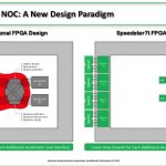
Built on TSMC’s 7nm node these new chips have several important innovations. Just as all our phone calls are now routed with packet technology, Achronix’s Speedster 7t will use a 2 dimensional arrayed network on chip (NoC) to move data between the compute elements, memories and interfaces. The NoC is made up of a grid of master and slave Network Access Points (NAPs). Each row/column operates at 256b @2.0Gbps, a combined 512 Gbps. This puts device level bandwidth in the range of 20Tbps.

The NoC supports specific connection modes for transactions (AXI), Ethernet packets, unpacketed data streams and NAP to NAP for FPGA internal connections. One benefit of this is that the NoC can be used to preload data into memory from PCIe without involving the processing core. Another advantage is that the network structure removes pressure during placement to position connected logic units near each other, which was a major source of congestion and floor planning headaches.

The NoC also allows the Achronix Speedster 7t to support 400G operation. Instead of having to run a 1000 bit bus at 724 MHz, the Speedster 7t can support 4 parallel 256 bit buses running at 506MHz to easily handle the throughput. This is especially useful when deep header inspection is required.

For peripheral interfaces, the approach that Achronix uses is to offer a highly scalable SerDes that can run from 1 to 112Gbps to support PCIe and Ethernet. They can include up to 72 of these per device. For Ethernet, they can run 4x 100Gbps or 8x 50Gbps. Lower rate Ethernet connections are also supported for back compatibility. They support PCIe Gen5, with up to 512 Gbps per port, with two ports per device.

The real advantage of their architecture becomes apparent when we look at the compute architecture. Rather than have separate DSPs LUTs and block memories, they have combined these into Machine Learning Processors (MLPs). This immediately frees up bandwidth on the FPGA routing. These three elements are used heavily together in machine learning applications, so combining them is a big advantage for their architecture.

AI and ML algorithms are all over the map on the need for mathematical precision. Sometimes large float precision is used, in other cases there has been a move to low precision integer. Google even has their own Bfloat precision. To handle this wide variety, Achronix has developed fracturable float and integer MACs. The support for multiple number formats provides high utilization of MAC resources. The MLPs also include 72Kbit RAM blocks, and memory and operand cascade capabilities.

For AI and ML applications, local memory is important, but so is system RAM. Achronix decided to use GDDR6 on their Speedster 7t family. It offers lower cost, easier and more flexible system design and extremely high bandwidth. Of course DDR4 can be used for less demanding storage needs as well. The use of GDDR6 allows each design to tune their memory needs, rather than being dependent on memory that is configured in the same package as the programmable device. Speedster 7t supports up to 8 devices with throughput of 4 Tbps.

There is a lot to digest in this announcement, it is worth looking over the whole thing. Looking back, this evolution will seem as obvious as how our old wired table top phones evolved into highly connected and integrated communications devices. The take-away is that this level of innovation will lead to unforeseen advances in end product capabilities. According to the Achronix Speedster 7t announcement, their design tools are ready now and they will have a development board ready in Q4.