This session will open the DAC IP Track at 10:30 on Monday “How PAM4 and DSP Enable 112G SerDes Design” in Room N264. I am very proud to chair this invited paper session, as it addresses one of the key pieces of design, enabling to exchange data flow at the highest possible data rate. It can be between two chips on the same board, we talk about short reach (SR) or even in the same package with very short reach (VSR) or on a backplane, the interconnect is named long reach (LR). In any case, the goal is to send a high number of data through serial link(s) after serialization (Ser) and receive it via Deserialization (Des), so the SerDes acronym.

Initially used in telecom networking in the end of 1990’s, the SerDes was based on LVDS I/O running at 622 Mbps. At that time I was working with TI as ASIC Marketing in charge of telecom customers in Europe, and TI has made numerous design-win, thanks to this 622 Mbps LVDS SerDes. If we make a fast forward to 2008, an IP vendor like Snowbush was comfortable with PCI Express 2.0, based on 5.0 Gbps link, and was developing a 10 Gbps SerDes to support 10G Ethernet. In 2019, several IP vendors have developed silicon proven 112G SerDes. This is simply a 180-multiplication factor for the data rate in 20 years!
If you compare with the evolution of the CPU frequency, from about 1 GHz in 1998 to less than 5 GHz today, you realize the performance made by SerDes architects and designers. As usual in the industry, this evolution is the result of hard work made by multiple teams of mixed-signal designers. Nevertheless, it’s interesting to notice that, most often, innovation was supported by start-up. When the technology was proven and shipping, these start-ups were acquired, like V-semiconductor by Intel in 2012, Nusemi by Cadence in 2017 or Silabtech by Synopsys in 2018.
We have mentioned mixed-signal designers as SerDes design has been based on analog techniques since the beginning, even when equalization or pre-emphasis were used, and these are known to be signal processing related. But Digital signal processing (DSP) was too power hungry to be a viable solution. Up to the last FinFET nodes (7 nm and below), where pure DSP techniques could be successfully applied, as Tony Pialis, CEO of Alphawave, will show in his paper. If you want to understand the state-of-the-art in term of SerDes architecture, you will love this paper!

The invited paper from Rita Horner will explain you how 56G and 112G PAM 4 PHY can be used to build 400G or 800G Ethernet interconnects at every level in data center: intra rack, inter racks, room to room or regional. In all the papers, the move from NRZ to PAM 4 modulation type will be clearly described -it’s a good opportunity to learn from real experts.
If you are not convinced about the importance in the industry of SerDes based, very high speed PHY, just think about the incredibly growing demand for data bandwidth. The adoption of future applications is conditioned to a fast access to the cloud for an ever-increasing bunch of data. If you want your smartphone to benefit from 5G capability to download a video or run a specific application, you expect the wireless base station to scale, and move data to the data center as fast as possible. Industrial IoT, IoT and automotive applications will also require moving large amount of data to and from the data center, and inside this data center, as fast as possible.
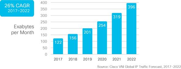
SerDes based, very high speed PHY, is a small piece of design, initially 100% analog based, relying now on DSP techniques to reach 112 Gbps link speed. It’s also an essential piece of Silicon allowing supporting the 26% CAGR for Internet bandwidth (according with Cisco, see above picture). This move to PAM 4 PHY is the main enabler to support 112 Gbps, if you want to know more about it, come to the DAC IP session on Monday 3rd in Room N264.
From Eric Esteve from IPnest
Share this post via:


Is Intel About to Take Flight?