As a professional conference attendee I look for the most meaningful way to spend my time and workshops is one of the best. Especially when a customer is involved and there is no bigger EDA customer than Intel, absolutely.
System Level Flows for SoC Architecture Analysis and Design
Speakers:
Swaminathan Ramachandran – CircuitSutra Technologies Pvt. Ltd.
Umesh Sisodia – CircuitSutra Technologies Pvt. Ltd.
Prassana Sadananda Rao – Intel Corp.
Organizer:
Umesh Sisodia – CircuitSutra Technologies Pvt. Ltd.
This workshop covers the latest trends and best practices in the domain of ESL methodologies for SoC Architecture, Co-Design, Co-Verification & raising the abstraction of chip design through High Level Synthesis. These advanced flows are enabled by using C, C++, SystemC, TLM2.0 along with traditional RTL flows.
Talk 1: Defining a SystemC Methodology for your Company
Swaminathan Ramachandran, CircuitSutra Technologies
As SystemC gains popularity in the fields of architecture evaluation, virtual platform development, SoC level verification, etc., more teams and companies want to explore, experiment and deploy it for their modeling use cases. While SystemC library provides the vocabulary and the nuts and bolts to build a useful and diverse set of models, it is sometimes too low level to be immediately useful. What is needed is a SystemC library analogous to Boost libraries in C++, for building blocks like memories, buses, registers, timers, etc. along with the infrastructure to quickly stitch them together into a working platform asap. Most of the Semiconductor companies who have successfully deployed SystemC, have developed their own tool independent methodology on top of SystemC, and they use it together with advanced modeling tools from EDA vendors. Such a library usually starts with basic building blocks, and over a period of time becomes a very rich collection of re-usable modeling components that can be re-used across various IP models, SoC variants, Modeling Use cases, business units, etc.
Any company looking to adopt SystemC in their flows should carefully conceptualize the development of such a methodology inhouse and can learn from the best practices being followed in the Industry. In this presentation, we will talk about what should be the content of such a methodology/library and how it should be conceptualized.
CircuitSutra has worked with leading semiconductor companies for more than a decade now and has participated in modeling projects from the stage of experimentation to pilot projects and to widespread adoption. We have an in-depth understanding of the best practices followed in the modeling domain.
Talk 2: System Flows in a “hybrid” Environment – Intel’s Approach
Prassana Sadananda Rao – Intel Corp.
The validation of SOCs at System level with full FW/SW stack in the pre-silicon stage itself is essential to accelerate SW readiness, improve RTL quality and overall shorten the product development cycle.
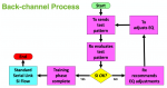
SoC FPGAs and Virtual Platforms (VP) are amongst the standard de-fact pre-Si solutions, However, each comes with its pro and cons: SoC FPGA has RTL accuracy but is available only after SoC integration is completed. VP arrives early but is more of an architectural model rather than RTL instantiation. To address this problem, our work describes an alternative leading-edge solution that starts at IP level itself. Single IP FPGA integrated into Virtual Platform (i.e., Hybrid IP-FPGA). Such a solution has the advantage of being available as soon as VP is ready. At the same time, it provides the IP RTL design with the necessary system-level context (i.e., interaction with FW/SW/Drivers of other components) which allows an early validation of IP design in an integrated environment instead of in isolation/standalone mode.
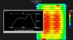
As a case study, we would present the results achieved on a complex PCI IP responsible for audio and sensing processing being integrated into one of the latest Intel SoC platforms. The IP was mapped to an IP FPGA, the SoC is modeled as a loosely timed Virtual Prototype and a hybrid layer plays the role of the glue logic for the two technologies. The overall Hybrid IP FPGA solution is proven to have a production level maturity that allowed the validation of complex system-level flows, such as security handshakes and power state transitions (reboot, S3, S4, and S5). Our case-study utilized only production-level SW/FW (the same that will be used on the real silicon) and enabled a tight interaction between the FPGA and other IPs of the platform thus exercising system-level flows which would be only visible when silicon is in the lab. This work set the foundation for making VP as the backbone of standalone IP RTL integration and candidates the proposed methodology as a breakthrough player in the pre-Si validation strategy of new SoC programs.
We will also discuss the challenges we faced while developing such a new methodology. In particular, the extra requirements that the VP model must satisfy to seamlessly integrate the hardware of the FPGA. As an example, the logic associated with the low-level hardware signals crossing the cutline of the two technologies must be modeled on VP with RTL accuracy in order to cope with FPGA expectations. Our future focus will be on developing VP interfaces in a scalable way to productize and scale such hybrid technology over a large set of different IPs.
Talk 3: Using High-Level Synthesis to Migrate Software Algorithms to Semiconductor Chip Designs
Umesh Sisodia, CircuitSutra Technologies
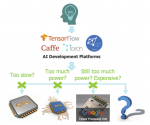
High-Level Synthesis (HLS) raises the abstraction of chip design beyond RTL. It enables the implementation of design functionality in high-level languages like C++/SystemC, and generates corresponding RTL using HLS tools. Synthesizable C++/SystemC code for design is very concise as compared to equivalent RTL code for the same design. Moreover, simulation of C++/SystemC models is much faster compared to RTL simulation. This allows significant productivity gains in the design and verification process. HLS also allows separation of functionality from architecture constraints and technology parameters, thus permitting code re-use across different variants of semiconductor chips, or across FPGA and ASICs.
HLS flows are more effective for algorithm centric designs. Nowadays we see new chip design requirements for emerging domains like 5G, Deep Learning, Vision, Image Processing, Speech, Audio processing etc. In these domains, there are many algorithms implemented in software, and several of these are available as open source.
In this talk, we will present an HLS based methodology to quickly migrate a software algorithm implemented in plain C/C++ to a hardware implementation in RTL for semiconductor chips (FPGA or ASIC). We will also cover a verification flow that allows the reuse of the original test suite of the software algorithm to verify the synthesizable C++/SystemC model as well as the final RTL. The untimed C++/SystemC models are also suitable to be used in Virtual Platforms, that allows embedded software development much before the chip is designed.
This methodology accelerates the pace of innovation, enables faster rollout of new chips, permits experimentation by quickly trying out the functionality in software and hardware, and taking high-level architecture decisions much earlier in the cycle.
Talk 4: SystemC Methodology for RISC-V Ecosystem
Umesh Sisodia, CircuitSutra Technologies
SystemC is a C++ library created for design and verification at the SoC and system level. It is widely used in the industry for system-level modeling, virtual prototyping, hardware-software co-verification, architecture & performance modeling, high-level synthesis, and functional verification.
RISC-V is an open-source processor ISA. Given that RISC-V ecosystem is in a nascent stage, yet there is widespread interest in the industry to explore the usage of RISC-V for various use cases. A robust modeling eco-system is necessary for the successful adoption of a new ISA, and in this context, a need exists for SystemC modeling infrastructure for RISC-V ecosystem. In this presentation, we will talk about some essential components required for anyone trying to deploy SystemC based methodologies for their RISC-V project.
CircuitSutra is an Electronics System Level (ESL) design IP and services company, headquartered in India, having development centers in Noida and Bangalore, and serves the customers worldwide. It enables customers to adopt advanced methodologies based on C, C++, SystemC, TLM, IP-XACT, UVM-SystemC, SystemC-AMS, Verilog-AMS. Its core competencies include Virtual Prototype (Development, Verification, Deployment), Architecture & Performance modeling, Co-simulation, Co-emulation, HLS, SoC & System verification.