I couldn’t attend the SPIE Advanced Lithography Conference this year for personal reasons, but last week Mike Lercel of ASML was nice enough to walk me through the major ASML presentations from the conference.
Introduction
In late 2018, Samsung and TSMC introduced 7nm foundry logic processes with 5 to 7 EUV layers, throughout 2019 both companies ramped up those processes and they are currently in high volume production. This year Samsung and TSMC are both ramping up 5nm foundry logic processes with 12 to 14 EUV layers and Intel is working on their EUV based 7nm process expected next year. Intel’s 7nm process should have densities comparable to Samsung and TSMC’s 5nm processes.
Samsung has also introduced their 1z DRAM process in late 2019 that initially was optical but then transitioned to a single EUV layer. In late March 2020 Samsung announced they had shipped one million DRAM modules with EUV based DRAMs. Samsung’s next generation DRAM process, the so called 1c generation DRAM is expected to have 4 EUV layers.
Clearly EUV is now accepted as best solution for critical layers for leading edge logic and DRAM production.
Mike discussed four presentations with me:
- Current production is being done with 0.33NA systems and ASML presented a current status and roadmap for these systems.
- The EUV source is a key component of the systems and the details of a new improved source were described.
- The status of efforts to produce a 0.5NA system improving resolution and productivity.
- ASML bought HMI and is continuing to develop their multi beam – Ebeam wafer inspection technology.
0.33NA Systems
The promise of EUV is summarized in figure 1.
Figure 1. Why ASML customers want EUV.
By the end of 2019 ASML had shipped 53 systems and over 10 million wafers had been exposed in the field. Figure 2 presents the systems shipped and wafers exposed by quarter.
Figure 2. EUV systems shipped and wafer exposed.
One particularly impressive aspects of figure 2 is the background photo that shows rows of EUV systems installed at an undisclosed customer site.
The current systems in the field are the NXE:3400B that have now demonstrated an average of >1,900 wafers per day (wpd) for one week, and >2,700 wpd for the best day.
Figure 3 illustrates that average availability is now reaching 85% with the top 10% of systems at 90%. 90% has long been the goal for the 3400B systems and ASML continues to work to tighten the 3400B system availability around 90%.
Figure 3. NXE:3400B availability trend.
ASML has now started to ship the NXE:3400C, the next generation system. The NXE:3400C features improved optics and mechanical throughput achieving an approximately 20% increase in throughput over the 3500B at 160 wafers per hour (wph) at a 20mJ/cm2 dose and 135 wph at a 30mJ/cm2 dose. The 3400B was always specified at a 20mJ/cm2 dose for throughput, the 30mJ/cm2 is in recognition of the need to increase dose as the feature sizes shrink. Authors note, I believe that even for 7nm foundry logic, the current doses are higher than 30mJ/cm2.
The 3600C features several improvements to the system to increase availability and the target is to reach 95%, the same availability that is achieved with DUV systems. The improvements will be discussed further in the paper on the source.
In mid-2021 ASML expects to ship the NXE:3600D with 160 wph throughput at a 30mJ/cm2 dose and longer terms there are plans to introduce a system with >=220 wph at a 30mJ/cm2 dose. The key to continual improvements in throughput are higher source power (see the EUV source section) and faster mechanical handling.
These throughput improvements are achieved while continually improving dose accuracy, overlay, CD uniformity and focus uniformity.
Figure 4. 0.33NA system roadmap.
EUV source
The largest availability loss causes on the 3400B system are the droplet generator and collector mirror, see figure 5.
Figure 5. Causes of availability loss.
The 3400C system directly addresses these issues with automated refills of the tin generator and a fast swap droplet nozzle and an easy access door for fast collector mirror swaps.
Figure 6. NXE:3400C availability improvements.
The lifetime of the collector mirror is also continuously improving while the power is also increasing.
Figure 7. Collector lifetime.
The net result of these improvements is a target for 95% uptime for the 3400C system in the field.
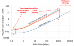
Looking forward at continued improvements in throughput ASML continues to drive up source power. Figure 8 illustrates the trend in source power. Note that the lag from research to high volume manufacturing is approximately 2 years so that we could possibly see a 500-watt source (the current source runs around 250-watts) around 2022.
Figure 8. Source power trend.
0.5NA System
The resolution of an exposure system is inversely proportional to NA. As critical dimensions shrink 0.33NA EUV systems will require multi-patterning to print the smallest features. The goal with the high NA systems is to match overlay and productivity of 0.33NA systems while enabling single pass lithography to be extended to smaller features.
The optical system for the 0.5NA systems is anamorphic, that is the magnification 4x in one direction and 8y in the orthogonal direction. This result in the field size being ½ of what it is for a 4x/4y system with the same reticle size. In order to achieve the high productivity goals the acceleration of the mask stage is 4x of a 0.33NA system and the acceleration of the wafer stage is 2x of a 0.33NA system.
Figure 9. 0.55NA system anamorphic lens.
Improvements in transmission in the fast stages result in improved throughput over the 0.33NA system at the same throughput. It should be noted here that some of the high speed sateg technology developed for the 0.55NA systems are being implemented on the 0.33NA systems to further improve throughput on those systems as well.
Figure 10. 0.55NA system throughput advantage.
Currently ASML is realizing the wafer and mask stage acceleration and finalizing the architecture. The main differences from the 0.33NA systems are the new optics system and faster stages although once again the faster stage technology is being used for the 0.33NA systems.
The 0.55NA systems also require better alignment and leveling. ASML is currently testing specific configuration to determine particle generation at high acceleration and are starting to gather some of the first sensor data.
ASML is also building out the infrastructure for the 0.55NA systems at various facilities around the world.
- ASML Wilton Connecticut is responsible for the reticle stages.
- At ASML headquarters in Veldhoven in the Netherlands the systems will be assembled.
- Ziess in Oberkochen Germany is responsible for the optics fabrication.
- ASML San Diego California is responsible for the source.
4 systems are currently on order with systems expected to be available in the 2022/2023 time frame.
Multibeam EBeam
ASML acquired HMI and has continued to pursue the HMI multibeam EBeam exposure technology. Ebeam inspection has very high resolution but is very slow taking approximately 2 hours to inspect 0.1% of a wafer.
The multibeam approach utilizes 9 beams in a 3 x 3 array all scanning simultaneously. Figure 11 illustrates the basic tool concept.
Figure 11. Multibeam EBeam system concept.
ASML has now demonstrated <2% cross talk between the beams and they are applying stage technology from their DUV exposure tools to improve the multibeam system throughput. They are targeting a 5-6x improvement in throughput and longer term are working on a 25-beam system.
Conclusion
EUV is now the solution of choice for critical lithography for leading edge processes. ASML continues to show progress both in the current 0.33NA generation systems and the development of next generation 0.55NA systems.
Also Read:
SPIE 2020 – Applied Materials Material-Enabled Patterning