

One of the side benefits of working with SemiWiki is that you get to meet a broad range of people and in the semiconductor industry that means a broad range of very smart people, absolutely. Recently I had the pleasure to meet Richard McPartland of Moortec. Richard and I started in the semiconductor industry at the same time but from across the pond as they say. Richard started at UK semiconductor pioneer Plessey in the early 1980s as an IC designer. The stories he can and does tell…
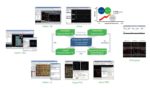
Richard and I are working on an upcoming webinar on optimizing power and increasing data throughput in advanced multi-core AI/ML/DL devices. Artificial intelligence, machine learning, and deep learning are touching just about every new design so this webinar will be a full one. Be sure and register to attend the event and you will get a link to the replay. Here is the webinar abstract:
If you are working on complex Artificial Intelligence (AI) or Machine Learning (ML) or Deep Learning (DL) designs using advanced node processes, you will understand the motivations for optimising CPU utilisation, device power and processing speed. Cutting-edge AI, ML & DL chips, by their very nature, are susceptible to intra-die process variability. Designers are often walking a fine line between optimal performance and failure.
This webinar from Moortec looks at how close real-time analysis of dynamic conditions, as well as identifying process corners, using embedded in-chip monitoring fabrics based on advanced node processes can greatly improve the power consumption, data throughput and computational performance of the overall system design.
Topics covered will include how tight dynamic guard-banding will enable improvement for the optimisation of multi-core utilisation, thermal load balancing and fine-grain SVS/AVS control, whilst the device is in mission-mode.
Due to their experience and dedication to In-Chip Monitoring, Moortec are able to support companies who are operating at the cutting edge of AI and Machine Learning chip design. Such companies have utilised Moortec’s highly accurate, highly featured sensors within their in-chip monitoring subsystem to ensure optimal performance and enhanced reliability.
Richard is also a fellow blogger. You can catch his musings on the Moortec blog site Talking Sense with Moortec.
He’s got two up thus far and they are very good:
Talking Sense with Moortec – Key Applications for In Chip Monitoring…In-Die Process Speed Detection
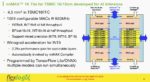
Chip designers working on advanced nodes typically include a fabric of sensors spread across the die for a number of very specific reasons. In this, the second of a three-part blog series Richard McPartland, Moortec’s Technical Marketing Manager continues to explore some of the key applications and benefits of these types of sensing solutions. In this instalment the focus is In-Die Process Speed Detection and why understanding in-chip process speed detection alongside thermal & supply conditions is essential if you want to maximise performance and power, improve reliability and ultimately reduce costs your cutting-edge design…
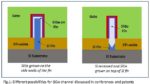
Talking Sense With Moortec – Key Applications For In Chip Monitoring…Thermal Sensing
The latest SoCs on advanced semiconductor nodes typically include a fabric of sensors spread across the die and for good reason. But why and what are the benefits? This first blog of a three-part series explores some of the key applications for In-chip thermal sensing and why embedding in-chip monitoring IP is an essential step to maximise performance and reliability and minimise power, or a combination of these objectives…
Moortec is one of the more collaborative companies I have worked with. They participate in most of the events I frequent and many more. It would probably be easier to list companies that they do not work with because their customer list is extensive. And when you do chip monitoring, analytics and optimization you get first hand experience with leading edge design challenges. So who better to partner with?


