RVN! 26 Banner revised (800 x 100 px) (600 x 100 px)

Can you really meet your SoC design schedule without a good GUI?

Can you really meet your SoC design schedule without a good GUI?
by Daniel Nenni on 08-31-2020 at 10:00 am

flow3 1

Talk to the members of a digital design team and you will always find two types of users. One who likes using the GUI while working on his design and the other who is passionate about using scripts and the command line options. This is akin to the two camps of users who either love either good old Vi/Vim or the ever versatile Emacs editor. But these days when there is every effort to meet the SoC tape-out deadlines, is there any place for a well-designed GUI, given the general belief is that using the GUI slows down the design process?

Using the GUI in some areas of the design flow such as floor-planning, simulation, debug etc. is quite common. But at the same time the GUI is getting ignored in a number of milestones of the SoC design flow where its usage could be quite useful. This is despite the fact that designers feel the need to use it but are handicapped by the way the GUI has been designed. For most engineers developing EDA software, functionality always gains a precedence over usability and aesthetics. One reason for this perhaps is the high complexity involved in developing the EDA tools. However, much has changed among the designers who use EDA tools to build their SoC designs. The higher expectation of the GUI has been set in part by the well designed and usable apps on the smart phone and other software tools which the designers use. But while the need to develop an easy-to-use GUI with good aesthetics has been embraced by software designers, it has been slow in gaining acceptance in the semiconductor world.

Whatever the cause may be for the lack of good GUI in the semiconductor world, few can deny that a well-designed GUI makes a big difference in improving the productivity of the designer. A good GUI makes the software approachable as it bridges functionality and aesthetics. This ensures better user engagement and improved productivity because it makes inherently hard to understand flows/tasks accessible and “easy”.

The other perspective one should also consider, is the GUI the designers have been habituated to. Most engineers are usually resistant to change as it means relearning and potentially recreating/testing their scripts, time which they can ill afford to waste given the tight design schedules. This is particularly true in areas such as physical implementation, simulation etc. EDA companies have found out the hard way that changing a GUI which the designers are habituated to can yield disastrous results in terms of usage. But this does not imply that a good GUI is not a necessity! In fact, on the contrary, a well-designed and intuitive GUI to address more aspects of the front end SoC design flow becomes all the more important as it ensures designers are cooperating in the most efficient way and collaborating in a well understood process.

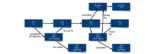
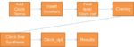
With increasing design complexity, design companies have married their EDA design tool flows with flow automation and efficient design handoffs to ensure software, hardware and verification teams can work in tandem and engage in productive collaboration. Emphasis is placed on re-usability and using a single source to automatically generate the desired correct-by-construction output consumed in various formats by different members of the design team lower down in the design flow. Setting up a design flow and automating as far as possible helps in performing well defined, potentially mundane tasks which are prone to human error. These include for example, virtual prototyping, defining the hardware-software interface, generation of structural RTL for top level wiring, insertion of test logic, documentation, design handoffs and creation of testbench and test vectors to verify the design. Doing this manually using scripts and command line across a design flow becomes rather tedious and error prone. With deadlines constantly looming before the design engineers, learning/relearning new methods to be more productive is a constant challenge.Consider the case of an IP in development. A common question often asked by engineers working on the IP is “Where is the golden source of information for my IP?” The answers change depending on whom you talk to. But given the design complexities, some parts of the design are auto generated while some are developed manually. Keeping track of the essential components and compiling the entire source in the desired format whenever a change is made, is easier said than done.  For example, the RTL designers need the updated RTL every time a change is made to the memory map or a change is made in the logical hierarchy to resolve congestion issues faced in the back end. Similarly, the verification engineers need an updated UVM test environment. And once the IP has been developed, packaging it with the necessary up-to-date documentation and datasheet is another hurdle which must be overcome. Managing this manually or through scripts poses a challenge which limits the productivity of the designer. This is a scenario wherein a well-developed GUI could increase the efficiency of designers considerably by an order of magnitude.

In the SoC world, any GUI without a datamodel has limited usefulness. While tool providers have used different types of data models to meet the GUI requirements, the semiconductor industry has been slowly adopting the IP-XACT standard owing to its capabilities. The fact that IP-XACT is an IEEE standard is equally important for most design companies. To see the benefits of using a datamodel, consider another example wherein an issue has been reported against an IP or a SoC. Resolving the issue involves first identifying the cause of the issue and then fixing the same. Debugging the issues quickly to find the root cause also helps save considerable time, something which a well-designed GUI can help considerably. Having a central representation of the IP such as interfaces, memory map, design connectivity etc. reduces the prospect of having to repeat the fix in multiple sources (HDL description, SW description, UVM description…). This central representation also helps finding corner case issues that are at the hardware-software boundary. With IP-XACT as a central datamodel, design companies can develop their own custom generators which they can leverage any time the datamodel is updated to generate the various outputs which are required.

But developing a good GUI is easier said than done. A number of factors needs to be considered while developing a GUI which addresses several parts of the SoC design flow. Some of these are

  • Providing a common UI environment which addresses different parts of the SoC design flow to ensure familiarity.
  • Intuitive and usable to make it easy for designers to use the tool
  • Optional built-in flows to guide designers through the various steps
  • Hooks to prevent mis-steps by the designers
  • A central data model which can meet the requirements of the complex design flows

To hasten the process of developing the SoC or IP using well defined flows, it becomes necessary to use solutions which are tried and tested and is part of a production flow in several companies. The new Design Environment from Magillem is one such solution which helps you to automate your design flows and build your designs faster. For more information on the Magillem products, visit www.magillem.com. Magillem customers include the top 20 semiconductor companies worldwide.

Magillem is a pioneer and the leading provider of IP-XACT based solutions aimed at providing disruptive solutions by integrating specifications, designs & documentation for the semiconductors industry. Using the solutions provided by Magillem, design companies can automate their design flows and successfully tape-out their designs faster at a reduced cost.

Magillem is one of the leading authorities on IP-XACT standard. It is also the Co-chair of the IP-XACT 2021 Accellera Working Group and an active member since the inception of the IP-XACT standard.


Data Management for the Future of Design

Data Management for the Future of Design
by Bernard Murphy on 08-31-2020 at 6:00 am

IP evolution min

Data management is one of those core technologies which is absolutely essential in any professional design operation. You must use a data management system; you just want it to be as efficient as possible. Most of us settled on one of a few commercial or open-source options. The problem seemed more or less solved. As usual in chip design, that problem has continued to scale beyond existing solutions. Now we have to contend with design databases on the order of petabytes – even a modest 50TB database will take 4 days or longer  to transfer to the cloud, a remote site or a foundry. Design activity is now much more distributed and interdependent. Now we have a new way to scale compute demand in the cloud, adding a new dimension in complexity to data storage and access.  Competitive advantage. demands a new approach to data management.

Start first with the implications for design in general, when there is increasing interest in agile methods and continuous integration. Components, like an IP or subsystem, can be evolving in multiple directions. Pulled into designs which create demands for fixes or derivative enhancements. Teams want to know status, whether perhaps they should switch to a more promising option for their needs. Components no longer evolve along a simple linear path. We need to be able to use the best available fit, as it becomes available.

Fast storage caches

Cost and latency are growing for design jobs. This is partly in compute – we always want faster compute engines. What was state-of-the-art yesterday looks barely acceptable today. But this is just as much of a problem in storage. Disks (cold storage) are slow and expensive and the IT world continues to advance. Now we can cache in much faster and cheaper NVMe memory (warm-storage), close to the compute engines, a very important consideration when you think of the constant syncing and re-syncing that may occur in-process in workspace data.

Storage hierarchies of this type are already supported in cloud services, which suggests a segue to hybrid cloud bursting, a popular method to push excess demand to the cloud as needed. Maybe you’re not ready to switch to all cloud, partly because you have a lot of sunk cost in your datacenter and you can’t move over until that’s depreciated. (Maybe you also have some residual security concerns. Different topic.)

Managing huge workspaces with the cloud

But there’s a data challenge with the hybrid approach. In many cases you have to carry along unmanaged data with the managed data, data generated in earlier steps which is needed in later steps. Physical data, corners, that sort of thing. This unmanaged data quickly dominated the total data size. Ftp or rsync methods to send all this data from your in-house NFS network to a cloud machine can become unmanageable. So much so that they might negate a lot of the advantage of running in the cloud.

Instead, using on-demand loading at a granular level, from the in-house network to cloud storage, can minimize the data that needs to be transferred. And once that data is uploaded to NVMe cache in the cloud, cold storage is no longer needed. Compute can work directly with the cache for higher performance at lower costs (you pay for cold storage in the cloud for as long as you are tying it up).

Data management analytics

There’s one more thing to get from this completely unified data management, across product groups, regions, in-house data center and clouds. You can track data analytics and access control much more easily. Data churn, phase completeness, check-in status, who is allowed access to licensed or otherwise privileged IPs. To see in one place where a project is really at. To see who might need additional help, to see who is adding unexpected royalty margins to your products.

You can get more detail from this IC Manage white paper, “A Blueprint for EDA Infrastructure for 2021 and Beyond”.

Also Read

Effectively Managing Large IP Portfolios For Complex SoC Projects

CEO Interview: Dean Drako of IC Manage


Protocol in Depth – USB

Protocol in Depth – USB
by Luigi Filho on 08-30-2020 at 10:00 am

Protocol in Depth USB

The USB protocol is a very complex protocol, so there is no way i can explain every detail in a post, but i can let much more easy to understand what happens in a bit level.

There isn’t much good material for easy understand about USB, so i made some assumptions for make easier explain everything. In this post i’ll explain how it goes.

The USB protocol doesn’t have a very well-defined layers, so i’ll divide in 3 layers: physical, protocol and framework. In this series each post will be about one of theses layers, how it’s shown in the figure below.

Of course this is how i choose to represent the USB layers, in the next posts:

  • In the next section I’ll talk about the physical layer.
  • After that I’ll talk about protocol layer.
  • In 4th section I’ll talk about the software in the framework.

Protocol in depth – USB – Physical Layer

In this layer I’ll explain about the Transceiver and Serial Interface Engine (SIE) but let me be clear, there some important concepts that I’ll not talk about like Endpoint, Host, Device, Hub.etc, and I’ll talk a little about the Low-Speed, Full-Speed and High-Speed, as I’m using the USB 2.0 specification I’ll not talk about SuperSpeed. There is no way that I can cover all topics in such small posts.

Transceiver

At each end of the data link between host and device is a transceiver circuit. The transceivers are similar, differing mainly in the associated resistors.

A typical upstream end transceiver is shown in first figure with high speed components omitted for clarity. By upstream, we mean the end nearer to the host. The upstream end has two 15K pull-down resistors.

Each line can be driven low individually, or a differential data signal can be applied. The maximum ‘high’ level is 3.3V.

The equivalent downstream end transceiver, as found in a device, is shown in second figure.

When receiving, individual receivers on each line are able to detect single ended signals, so that the so-called Single Ended Zero (SE0) condition, where both lines are low, can be detected. There is also a differential receiver for reliable reception of data.

Some signaling that the transceiver need to be aware is described below:

  • Speed identification

At the device end of the link a 1.5 kohm resistor pulls one of the lines up to a 3.3V supply derived from VBUS.

This is on D- for a low speed device, and on D+ for a full speed device.

(A high speed device will initially present itself as a full speed device with the pull-up resistor on D+.)

  • Line States

Given that there are just 2 data lines to use, it is surprising just how many different conditions are signaled using them:

  • Detached

When no device is plugged in, the host will see both data lines low, as its 15 kohm resistors are pulling each data line low.

  • Attached

When the device is plugged in to the host, the host will see either D+ or D- go to a ‘1’ level, and will know that a device has been plugged in.

The ‘1’ level will be on D- for a low speed device, and D+ for a full (or high) speed device.

  • Idle

The state of the data lines when the pulled up line is high, and the other line is low, is called the idle state. This is the state of the lines before and after a packet is sent.

  • J, K and SEO States

To make it easier to talk about the states of the data lines, some special terminology is used. The ‘J State’ is the same polarity as the idle state (the line with the pull-up resistor is high, and the other line is low), but is being driven to that state by either host or device.

The K state is just the opposite polarity to the J state.

The Single Ended Zero (SE0) is when both lines are being pulled low.

The J and K terms are used because for Full Speed and Low Speed links they are actually of opposite polarity.

All details is shown in the figure below:

  • Single Ended One (SE1)

This is the illegal condition where both lines are high. It should never occur on a properly functioning link.

  • Reset

When the host wants to start communicating with a device it will start by applying a ‘Reset’ condition which sets the device to its default unconfigured state.

The Reset condition involves the host pulling down both data lines to low levels (SE0) for at least 10 ms. The device may recognise the reset condition after 2.5 us.

  • EOP signal

The End of Packet (EOP) is an SE0 state for 2 bit times, followed by a J state for 1 bit time.

  • Suspend

One of the features of USB which is an essential part of today’s emphasis of ‘green’ products is its ability to power down an unused device. It does this by suspending the device, which is achieved by not sending anything to the device for 3 ms.

Normally a SOF packet (at full speed) or a Keep Alive signal (at low speed) is sent by the host every 1 ms, and this is what keeps the device awake.

A suspended device may draw no more than 0.5 mA from Vbus.

A suspended device must recognise the resume signal, and also the reset signal.

  • Resume

When the host wants to wake the device up after a suspend, it does so by reversing the polarity of the signal on the data lines for at least 20ms. The signal is completed with a low speed end of packet signal.

  • Keep Alive Signal

This is represented by a Low speed EOP. It is sent at least once every millisecond on a low speed link, in order to keep the device from suspending.

SIE

What is the SIE? A typical function USB hardware interface is shown below

The SIE is the frontend of this hardware and handles most of the protocol signaling. The SIE typically comprehends signaling up to the transaction level. The functions that it handles could include:

  • Packet recognition, transaction sequencing
  • SOP, EOP, RESET, RESUME signal detection/generation
  • Clock/Data separation
  • NRZI Data encoding/decoding and bit-stuffing
  • CRC generation and checking (Token and Data)
  • Packet ID (PID) generation and checking/decoding
  • Serial-Parallel/ Parallel-Serial Conversion

A typical implementation of an SIE with these functions takes about 2500 gates. So the module itself is fairly small; and the functionality is straightforward. In spite of this apparent simplicity, it is possible to end up with a design that doesn’t work reliably i.e. a design which is not robust. I will point out some reasons for problems from a design.

  • Sources of robustness problems

The primary source of robustness problems is the existence of multiple clock domains in the SIE, some of which are asynchronous to each other. If signaling between these domains doesn’t adhere to synchronization rules, intermittent problems can result. These problems are invariably difficult to track down and fix.

Other areas which have the potential for robustness problems include:

  • out-of-band signal handling on per-packet basis
  • bit stuffing/unstuffing
  • special casing for setup, iso etc
  • special casing for low speed
  • suspend /resume support

The following text will review some of these areas in turn and discuss techniques to address the problems.

  • Multiple clock domains

The typical SIE has to deal with four clock zones in three domains:

  1. · USB host 12Mhz clock or receive clock
  2. · internal 4x clock (48Mhz) and transmit clock (divided by 4 version)
  3.  · SIE backside clock or interface clock
  • Race Conditions in the transmit domain

The clock zones in the second domain are synchronous; however race conditions could occur in signaling between the 1x and 4x sub domains because the 1x clock is derived from the 4x clock. This may be a bigger problem in some target technologies than in others. The problem is exacerbated by the need to switch the hardware between transmitter and receiver clocks.

Since the USB is half duplex several of the modules in the SIE can be shared between transmit and receive e.g. the crc logic . Since every USB transaction includes receive and transmit phases, the state machines carry state between the phases. So there is a need for a means to reliably multiplex between receive clock and transmit clock.

  • Packet delimiters and out of band signaling

Precise detection of packet delimiters is crucial for robust SIE operation. Each packet has a start delimiter (or sync) and end delimiter (or EOP). The nominal sync field consists of an NRZI KJKJKJKK pattern. Even though this is an in band (made up of differential signals) pattern, the initial bit may be distorted due to hub turn on behavior .

  • Bit stuffing and unstuffing

Bit stuffing and unstuffing can be implemented by putting the state machines and datapath on hold while stuffing or stripping the extra bit. Bit unstuffing near the EOP needs to be handled carefully as explained above.

Although most transactions are three phase, ISO transactions are only two phase and the state machines need to comprehend this. Similarly SETUP transactions are identical to OUT transactions except that they cannot be NAKed or STALLed. The data buffering and the state machines need to take this into account. Data toggle sequencing logic at a bidirectional endpoint should take into account the specific requirements for the starting toggle sequence of each stage of a control transfer.

Low speed signaling is identical to full speed signaling except for the inversion of polarity. But low speed devices need to comprehend that while most data entities are defined in terms of number of bits, the se0 width for reset is not. Low speed devices should also be able to handle keep-alive signals (bare EOPs) correctly.

USB Protocol in Depth – Protocol Layer

In this article I’ll try my best to explain the most part of the protocol layer of USB specification.

I’ll talk a little about the transfers, but will not cover a lot, maybe I’ll make an article just about the transfers, but what you need to know is that for each use you have a different type of packages.

In the last section we could check the physical layer that will interface the connector and will work together with the SIE, but as the SIE isn’t very well define in the specifications this could lead to great confusion, as many manufacturers could implement the SIE together with the Protocol layer, or some of the functions of the protocol.

As what I define about SIE in the last post, SIE will handle the signaling and the interface with protocol layer, to let things easier let’s consider that the SIE will interface with protocol layer by UTMI (USB 2.0 Transceiver Macrocell Interface) or ULPI (UTMI+ low pin interface), that’s the usually you can find in most standard USB 2.0/3.0 transceiver integrated circuits.

Other consideration is that I’ll need to define the 4 types of transactions that exists on USB protocol:

  • Control Transfers Used for sending commands to the device, make inquiries, and configure the device.
  • Interrupt Transfers Used for sending small amounts of bursty data that requires a guaranteed minimum latency.
  • Bulk Transfers Used for large data transfers that use all available USB bandwidth with no guarantee on transfer speed or latency.
  • Isochronous Transfers Used for data that requires a guaranteed data delivery rate. Isochronous transfers are capable of this guaranteed delivery time due to their guaranteed latency, guaranteed bus bandwidth, and lack of error correction. Without the error correction, there is no halt in transmission while packets containing errors are resent.

The protocol layer manages the end-to-end flow of data between a device and its host. This layer is built on the assumption that the link layer guarantees delivery of certain types of packets and this layer adds on end to end reliability for the rest of the packets depending on the transfer type.

Here we will discuss the following concepts in detail:

  • Types of packets
  • Format of the packets
  • Expected responses to packets sent by the host and a device
  • Support for Streams for the bulk transfer type
  • Timing parameters for the various responses and packets the host or a device may receive or transmit

One first thing if you look at the USB communication from a time perspective, it contains a series of frames, in your time slot. Each frame consists of a Start of Frame (SOF) followed by one or more transactions. Each transaction is made up of a series of packets. A packet is preceded with a sync pattern and ends with an End of Packet (EOP) pattern. At a minimum, a transaction has a token packet. Depending on the transaction, there may be one or more data packets and some transactions may or may not have a handshake packet.

Packet Types can potentially represent four packet types:

1.      Token packets

  • Initiate transaction
  • Identify device involved in transaction
  • Always sourced by the host

2.      Data packets

  • Delivers payload data
  • Sourced by host or device

3.      Handshake packets

  • Acknowledge error-free data receipt
  • Sourced by receiver of data

4.      Special packets

  • Facilitates speed differentials
  • Sourced by host-to-hub devices

I’ll cover Token, Data and Handshake packets, special packets will be cover maybe in a future article about Hubs, leave a comment if you want an article about USB HUB.

Token packets always come from the host and are used to direct traffic on the bus. The function of the token packet depends on the activity performed, the format for a token packet is shown in the image below.

Another token packet is a SOF (start of frame) packet, show in the figure below

Data packets follow IN, OUT, and SETUP token packets. The size of the payload data ranges from 0 to 1024 bytes depending on the transfer type. The packet ID toggles between DATA0 and DATA1 for each successful data packet transfer, and the packet closes with a 16-bit CRC. The format is shown in the figure below

Handshake packets conclude each transaction. Each handshake includes an 8-bit packet ID and is sent by the receiver of the transaction, the format is shown in figure below

I know that I’m missing more information about each bit in PID, ADDR, ENDP, DATA, Frame Number and CRC5/16, but this article is already to extensive, if you want know more details, leave a comment.

How the USB is a protocol with handshake, usually with some packets will be expect some responses, to simplify let’s consider that always an token will be sent, followed by a data packet or receiving a data packet always will be a handshake packet involved, how the article is going a little extend, leave a comment if you want an article about the transfers.

All this is valid for each type of transfers, which can be a control, interrupt, bulk or isochronous transfers.

Other concept is that each 1ms is a frame that contain a SOF and can contain many packets. In high speed an SOF is sent out every 125 us and frame count is only incremented every 1ms.

USB in Depth – xHCI

In terms of USB Standards, xHCI will be implemented in the Host side of the USB communication, from the Endpoint to the software driver.

Have in mind that, we are in the Host side of an USB 3.x version (With “SuperSpeed”) but still compatible with USB 2.x and 1.x. The xHCI was created to replace OHCI, UHCI and EHCI. Other important thing is that, all host controllers need to implement hub functions, all theses things I don’t cover in my last articles, and I’ll not cover in this, if you want, leave a comment and I’ll cover theses topics, this topic is created due a comment!

Another point is that in USB3.x you have a PIPE interface too instead of only UTMI+.

The first point you need to consider is the Endpoint, i talked a little about Endpoint in the others articles, here and here. Everything from the pins until the Endpoint it’s valid and the same here. But there is a new “player” the “Rings”, and there is three of them: Transfer Ring, Event Ring and Command Ring and each Endpoint has his Transfer Ring.

Another new concept is Transfer Request Block, that is a data structure construct in memory by the software to transfer a single physically block of data between host memory and the Host Controller. Contain a single data buffer pointer, size of the buffer and some additional control information.

Same new concepts are, Device Contexts and the Device Context Base Address Array. The Device Context is used to report the device configuration and state information to the system software and consists of 32 data structures ( index = 0 for Slot Context and the remaining (1 to 31 are Endpoints Context). The Device Context Base Address Array is the based lookup table for accessing the Device Context in each slot.

I’ll focus in the data transfer and not cover Event Ring Segmented Table, Event Ring, Command Ring. Other thing considering in the standard is an PCI config space, but I will not cover, is away out of this scope.

Other thing to consider is the registers of the xHCI, they are:

  • Doorbell Array – The Doorbell Array (up to 256 Registers of 32 Bits) is defined in the array for each Device Slot. System Software utilizes theses registers to notify the Host Controller that it has Device Slot related work for the Host Controller to perform.
  • Runtime Registers – Is referred as Runtime Base too, and each register multiples of 32 bits in length, is used to control microframe and interruptions.
  • xHCI Extended Capabilities – If the Host Controller implements any extended capabilities, it specifies a non-zero value in the xHCI Extended Capabilities Pointer field
  • Operational Registers – The Operational Registers, referred as Operational Base, are registers to support the operation of the USB xHC.
  • Capability Registers – This registers specify the limits and capabilities of the host controller implementation

Host Controller Initialization

When the system boots, host controller is enumerated, assigned a base register for the xHC register space and the system software sets the Frame Length Adjustment (FLADJ) register to a system-specific value.

Some tasks of the system software need to perform are:

  • Initialize the system I/O memory maps, if supported
  • After hardware reset, wait until the Controller Not Ready flag in the USBSTS is ‘0’ before writing any xHC Operational or Runtime Register
  • Program the Max Device Slots Enabled field in CONFIG register
  • Program the Device Context Base Address Array Pointer (DCBAAP) register
  • Define the Command Ring Dequeue Pointer
  • Initialize Interrupts
  • Write the USBCMD to turn the Host Controller ON.

At his point the host controller is up and running and the Root Hub ports will begin reporting device connects, etc, And the system software may begin enumerating devices.

Just remember that USB2.x devices require the port reset process to advance the port to the Enabled state.

USB Device Initialization

The USB Device initialization process is the same, whether the device attached is an HUB or any another Function.

After a Hardware Reset, HCRST, or command to the PLS = RxDetectState, all Root Hub ports shall be in Disconnected state and when a USB device is attached to a port that is in Disconnected state all the protocol process will start.

I will not go into details in this step, it’s a long process that you need to be sure to follow all steps for correct operation, you can check the standard to get all steps.

Transfer Request Block (TRB)

I’ll say that to start understand how everything get together you need to understand the TRB’s, they will make the interface from what you know about USB transfers (Isoch,Interrupt, Control and Bulk) to the xHCI software and hardware controllers. Each of the USB transfers have one TRB related, the template is shown in the image below.

Each transfer will have your own parameters, status, control, etc fields, with this basic structure.

The TRB Ring make the management of the TRB’s. The TRB Ring is a circular queque of TRB data structures and there is 3 basic types: Transfer, Event and Command.

Command Interface

The Software places commands on the Command Ring, through the Command Ring Control Register (CRCR), then rings the Host Controller Doorbell Register to notify the hardware. Some commands are:

  • Enable/Disable Slot
  • Configure/Reset/Stop Endpoint
  • Reset Device
  • Force Event/Header

Doorbells Registers

The doorbells are an array of 256 32-bit registers that reside in MMIO space and are indexed by device slot Id. Each Doorbell has an Endpoint associated to it.

Conclusion

The xHCI will manage all the USB transfers in the host, making the bridge between hardware and software.

With theses definitions in mind, i think you can go over the standard and understand better, as always that’s no possible to cover all in theses small articles.

You can always leave a comment, can ask to cover any topic as few people already did it, this topic included. The next Topic will be PCIe.


Smartphone Processor Trends and​ Process Differences down through 7nm

Smartphone Processor Trends and​ Process Differences down through 7nm
by Fred Chen on 08-30-2020 at 6:00 am

Transistor density process for Huawei and Apple

This comparison of smartphone processors from different companies and fab processes was originally going to be a post, but with the growing information content, I had to put it into an article. Here, due to information availability, Apple, Huawei, and Samsung Exynos processors will get the most coverage, but a few Qualcomm Snapdragon processors will also be included in some comparisons.

The Processes
The processors compared here will be fabbed at Samsung and TSMC, starting from 14/16nm and going down to 7nm EUV versions.

What’s being compared
Die width and die height will be compared among the processors from each of the different companies. Transistor density data (available only for certain processors) will be used for process comparisons.

Smartphone processor die sizes
In Figure 1, the die size trends for the smartphone processors from Samsung, Huawei, and Apple are separately plotted vs. the different processes used.

Figure 1. Die size trends vs. process for Samsung (left), Huawei (center), and Apple (right). Qualcomm is added at far left for die area only.

For Samsung, the introduction of 7LPP enabled a die height reduction. However, unexpectedly, its 91.83 mm2 area does not give the smallest die area among all the processors considered here. Among 7nm processors, the smallest processor area goes to the Snapdragon 855 (73.3 mm2), fabricated on TSMC’s original 7nm process. The Snapdragon 835 was even smaller at 72.3 mm2, but is made on Samsung’s 10nm (LPE) process, with a much lower transistor density. The other 7nm EUV processor, the Huawei Kirin 990 5G made at TSMC, also had enlarged die size (113.3 mm2), but this can be attributed to new features in the processor design [1].

Die width is not trending down with advanced processes. This will be a concern for the use of EUV, as discussed in detail later. With shrinking cell track heights, the impact of illumination rotation will become more significant.

Transistor Density
Transistor density is plotted for Huawei and Apple processors vs. process in Figure 2.

Figure 2. Transistor density vs. process for Huawei (left) and Apple (right).

The biggest surprise here comes from TSMC’s 7nm EUV process NOT giving the highest transistor density. Among the Kirin processors shown, the Kirin 980 gives the highest density (93.1 MTr/mm2) which is higher than the Kirin 990 5G at 90.9 MTr/mm2. The other processor which beat this value is the Snapdragon 855, coming in at 91.4 MTr/mm2.

The highest densities and smallest die sizes so far at 7nm were realized on TSMC’s first 7nm process. The TSMC 7nm process in fact has a shorter high-density track height (240 nm) [2] than Samsung’s 7nm EUV process (243 nm) [3]. The Exynos 990 in fact used the high-performance track height, which is 270 nm. These actually offset the potential benefits of a smaller metal pitch.

Going to 5nm, track height is expected to be reduced, especially with 6-track cells becoming available.

Track height reduction consequences for EUV
Samsung’s 7nm EUV process offers 270 nm (7.5-track) and 243 nm (6.75-track) cell heights. The 5nm continuation of this process also offers a 216 nm (6-track) cell height [4]. The process is considered a continuation because the minimum metal pitch remains at 36 nm. The minimum metal pitch has a strong influence on the EUV process, as it sets a preferred illumination angle (whose sine = 0.1875 to be exact). However, this illumination angle is rotated across the die, up to 18.2 degrees at 13 mm from the center [5]. Since the die width for the Samsung Exynos processors shown in Figure 1 have been in the neighborhood of 10.7 mm, we should consider the effect of a 7.5 degrees (=18.2 degrees x 5.35 mm/13 mm) maximum rotation at the chip edge compared to the center. The effect is not so profound for the 36 nm pitch itself but more so for the track height being the true pitch. The much larger track height as pitch generates a more complex diffraction order spectrum. The phase difference between the 0th and 1st orders is normally not affected significantly by the incident angle “shadow” in the x-direction but the rotation changes this (Figure 3).

Figure 3. The impact of 7.5 degree rotation of illumination for 243 nm (top) and 216 nm (bottom) track heights. For the rotated case, defocus generates a larger range of phase errors across the pupil (different angle tils in x-direction). Thus, images at the die edge go out of focus more easily.

The lines in the 6- or 6.75-track cell will go out of focus more easily at the die edge. The effect is more severe not only as the minimum metal pitch decreases but also as track height decreases, due to larger path differences between consecutive orders at smaller pitches.

What to expect in the future
Now that Huawei’s supply from TSMC has been interrupted, there is a possibility it will rely on a new foundry source within China, such as SMIC [6]. It may try to first replicate the success of the Kirin 980 domestically, as mainland China has not yet reached the ‘7nm’ stage in its technology development. In the meantime, both Apple and Qualcomm continue to be successful in their work with TSMC on the 7nm ‘P’ process. With some reduction in popularity of the Exynos processor series, Samsung’s Exynos processor designs may be swapped for a non-customized ARM core design [7]; it remains to be seen if that can revitalize in-house processor design. Otherwise, Samsung’s phones can still be sold with Qualcomm’s Snapdragon processors exclusively.

References
Processor die size and transistor density information can be found from Techinsights (Exynos 8895, Exynos 9810, Exynos 990, A13, Kirin 990 5G, Snapdragon 835, Snapdragon 865), Anandtech (A9, A10X, Kirin 960, Kirin 980), Chiprebel (Exynos 9820, A11), Wikichip (A12, Kirin 970, Kirin 990 4G, Snapdragon 855).

[1] https://www.anandtech.com/show/14851/huawei-announces-kirin-990-and-kirin-990-5g-dual-soc-approach-integrated-5g-modem

[2] https://fuse.wikichip.org/news/2408/tsmc-7nm-hd-and-hp-cells-2nd-gen-7nm-and-the-snapdragon-855-dtco/

[3] https://fuse.wikichip.org/news/1479/vlsi-2018-samsungs-2nd-gen-7nm-euv-goes-hvm/

[4] https://fuse.wikichip.org/news/2823/samsung-5-nm-and-4-nm-update/

[5] A. V. Pret et al., Proc. SPIE 10809, 108090A (2018).

[6] https://www.eetasia.com/how-smic-can-keep-up-with-advanced-process-technologies-part-2/

[7] https://www.notebookcheck.net/Why-ARM-s-Cortex-X1-cores-likely-for-Samsung-s-Exynos-1000-possible-future-Pixel-SoC-too.466957.0.html

Related Lithography Posts


Making Full Memory IP Robust During Design

Making Full Memory IP Robust During Design
by Daniel Payne on 08-28-2020 at 10:00 am

64Mb SRAM example, memory IP

Looking at a typical SoC design today it’s likely to contain a massive amount of memory IP, like: RAM, ROM, register files. Keeping memory close to the CPU makes sense for the lowest latency and highest performance metrics, but what about process variations affecting the memory operation? At the recent DAC conference held online I was able to get some answers by attending a Designer Track session entitled, Ensuring Design Robustness on Full Memory IP using Sigma Amplification, presented by Ashish Kumar, ST Microelectronics.

Ashish showed that for a 64Mb SRAM there are over 50,000 MOS devices, 100K nodes and 400K extracted RC parasitic elements, and such a large netlist requires a large number of Monte Carlo simulation runs to ensure robustness. The blocks comprising this SRAM include Bitcells, Local I/O, row decoders, local control, global I/O and global control, as shown below:

There are 64M bit cells and they require a 6.3 sigma analysis, and with classical Monte Carlo it requires 6.4B simulations to achieve a 99% yield, something that cannot be accomplished in a reasonable run time, so clearly we are in trouble to achieving a robust design. The other blocks inside of the memory have lower counts and corresponding lower sigma goals.

The actual bit cell schematic uses seven MOS transistors, and for a read operation the signal SAEN pulses high, then the Bit Line (BL) and Bit Line Bar (BLB) nodes start to diverge in value creating Vdiff. The larger the value of Vdiff the more stable and robust our memory cell design is.

Using a traditional SPICE circuit simulator like HSPICE from Synopsys you could get 100 Monte Carlo runs in a reasonable amount of time, or with the high-capacity CustomSim tool maybe 1,000 runs, but both of those fall short of the 6.4B runs required get our robust design goals met. Process variations are no longer occurring with Gaussian distributions, see the plot below for the areas circled in Brown color, so to get a robust design we need a method to statistically fit these distributions.

The value of Vdiff can be measured while running Monte Carlo simulations with a varying number of runs, and we find that with more runs the lower the value of Vdiff becomes. For 10,000 runs we find that the value of Vdiff falls to 260mV, but that it takes about 50 hours for circuit simulation to complete.

A normal Gaussian distribution is shown in Blue, but we really want to look at the tail of the distribution so if a statistical sample is taken in the tail region as shown by the Red curve then fewer simulations are required. This technique is called Sigma Amplification.

Within the Synopsys circuit simulators you can choose a Sigma Amplification value, and they recommend a value of 2 or smaller (shown in Grey) in order to reach an affordable sample size.


In the HSPICE GUI a designer can reach 5.8 Sigma for a memory block, but instead of taking 109,522,300 Monte Carlo runs it only takes 1,000 runs by using a Sigma Amplification of 1.7:

The minimum value of Vdiff using traditional Monte Carlo with 1,000 runs is 270mV, while Vdiff is calculated to be 140mV when using a Sigma Amplification value of 1.67, which proves that we are finding even more worst case samples that are not following a normal distribution. In just 5 hours we know that Vdiff has a much lower value than before using Sigma Amplification, something that was not possible with traditional Monte Carlo simulations.

Comparing Vdiff versus distributions, consider three approaches:

  • Real distribution – traditional Monte Carlo with Gaussian distribution
  • Extrapolated with Gaussian distribution
  • Sigma Amplification

Using real distribution with 10,000 samples we can only achieve +/- 4 sigma results. If we  extrapolate with gaussian distribution, then Vdiff can reach +/- 5 sigma in 1,000 samples, but our  Vdiff values become inaccurate, so faster incorrect answers. With the Sigma Amplification approach we can reach +/- 5 sigma results, using only 1,000 samples while maintaining acceptable accuracy levels.

Another way to visualize these three approaches is to plot Vdiff as a function of Sigma. The Real Distribution is shown in Blue color, and the most accurate comparison is Sigma Amplification in Grey, while the least accurate approach is Extrapolated with Gaussian distribution in Purple.


Summary

Memory IP design is important for modern SoCs, so getting robust IP blocks is quite important to reliable operation over the product lifetime, but using traditional Monte Carlo approaches with Gaussian distributions during the design phase just takes too much time. Fortunately for us, there are approaches to focus on the tail regions to uncover the worst-case conditions by using a statistical distribution approach. Synopsys calls their approach Sigma Amplification and the theory is borne out on real memory IP, so designers can now achieve a much higher sigma goal with fewer Monte Carlo runs.

Also Read:

ARC Processor Virtual Summit!

Synopsys Webinar: A Comprehensive Overview of High-Speed Data Center Communications

Accelerating High-Performance Computing SoC Designs with Synopsys IP


CEO Interview: Charlie Janac of Arteris IP

CEO Interview: Charlie Janac of Arteris IP
by Daniel Nenni on 08-28-2020 at 6:00 am

charlie janac


Charlie Janac is president and CEO of Arteris IP where he is responsible for growing and establishing a strong global presence for the company that is pioneering the concept of NoC technology. Charlie’s career spans over 20 years and multiple industries including electronic design automation, semiconductor capital equipment, nanotechnology, industrial polymers and venture capital.

In the first decade of his career, he held various marketing and sales positions at Cadence Design Systems (NYSE: CDN) where he helped build it into one of the ten largest software companies in the world. He joined HLD Systems as president, shifting the company’s focus from consulting services to IC floor planning software and building the management, distribution and customer support organizations. He then formed Smart Machines, manufacturer of semiconductor automation equipment and sold it to Brooks Automation (NASDAQ: BRKS). After a year as Entrepreneur-in-Residence at Infinity Capital, a leading early-stage Venture Capital firm, where he consulted on Information Technology investment opportunities, he joined Nanomix as president and CEO helping build this start-up nano-technology company. Mr. Janac holds a B.S. and M.S. degree in Organic Chemistry from Tufts University and an M.B.A from Stanford Graduate School of Business.

Why is on-chip interconnect important for SoC innovation?
System-on-chip architectures are rapidly changing because we are moving from “data processing” chips to SoCs able to execute “decision making” models. The on-chip interconnect is the logical and physical means to create the SoC architecture so the importance of the network-on-chip (NoC) interconnect has increased as the need for architectural innovation has grown. As machine learning capabilities are being incorporated into a wider variety of SoCs, the new dataflow patterns driven by these heterogenous processing systems are driving far-reaching innovation in interconnect IP. Cache coherency is becoming more common to simplify software development and reduce system latency in these multicore SoCs. And the size of these machine learning subsystems is sometimes forcing chip architects to split their designs over multiple dies or packages which is causing innovation in chiplet connectivity IP that is tightly couple with, or even within, the interconnect. The bottom line is that interconnect IPs are becoming more complex and important as the number and complexity of SoC IP blocks grow and data flows become more sophisticated due the machine learning and cache coherent traffic.

What developments do you see that Arteris IP is able to address?
We’re at a very exciting time because an important ingredient for performant SoCs has clearly become the on-chip interconnect and all the SoC architectural changes by our customers are influencing our technology development. Soon you’ll see on-chip cache coherency interconnect IP with features such as multilevel caching of metadata and ability to handle multiple cache coherency protocols for processors of different characteristics – more specifically, both ARM CHI and ACE protocols simultaneously. Interconnect requirements for machine learning subsystems and SoCs have inspired specialized features such a broadcast and multicast, and the generation of large meshes to improve delivery of machine learning SoCs. In other types of SoCs, target/initiator type “tree” topologies are more efficient in terms of area, power and latency so flexibility is a key interconnect aspect.

System level and design methodology considerations also guide our technology. Tighter integration of NoC interconnects and industry standard memory controllers creates the opportunity for end-to-end quality-of-service (QoS), i.e., system-level runtime bandwidth and latency regulation, and ECC data protection. And we’re tightening the links between the logical/RTL and physical/floorplan “views” of NoC interconnects which reduces the number of place and route design cycles, shortening engineering schedules. In summary, Arteris IP is a critical enabler in the realization of these new SoC architectures through our unified cache coherent and non-coherent interconnect solutions based on network-on-chip technology.

How has importance of NoC interconnect changed since 2016?
First, SoCs have become so much larger that the need for interconnect scalability has greatly increased. The numbers of IP blocks connected in our customers’ chips is now often in the hundreds. And dataflow complexity is increasing as many of these IP blocks are being combined into hierarchical subsystems. Many NoC interconnect instances now exceed 10M gates, which used to be the size of an entire chip a few years ago. With die size, comes high power consumption, and our NoC interconnect technology has highly effective gating and power management functionality to minimize power consumption.

Second, on-chip dataflow requirements have changed and often conflict with each other. For example, on-chip bandwidth demands for some of our customers’ designs exceed 1 terabit/second, but these designs also often have portions with critical latency requirements, such as when processing elements are communicating with memories. But it’s not all about on-chip bandwidth. The importance of latency optimization, not just on-chip bandwidth, has grown as demands for overall SoC performance have increased, and without the configurable flexibility inherent in our NoC technology these requirements would inexorably conflict. Being able to model and implement such different use cases and then determine a NoC architecture that meets them both simultaneously puts pressure on the NoC EDA tool sets to deliver maturity, usability and required automation features. Physical awareness provides the knowledge of location and distance between NoC elements in relation to the other IP block locations on the chip floorplan, which supports latency optimization and automated pipeline insertion for rapid timing convergence estimation.

Third, increasing overall SoC performance requires running the interconnect and its associated on-chip memories at higher frequencies, sometime at the same clock frequency as the fastest processing element IP. But these designs often need to run at much lower frequencies to save power when dataflow is quiescent. State of the art interconnect must be able to support low frequencies for low power modes and chip designs all the way to 2Ghz+ for high performance designs.

Fourth, automated verification uses the information from NoC generation to automatically output test benches in a fraction of time required for manual verification.

The expense of delivering state-of-the-art interconnect solutions has also increased because NoC R&D investment must keep pace with overall SoC innovation. Of course, the value of NoC interconnect has increased so much that it is now one of the most important IPs in the SoCs. NoC interconnect has become a key determinant of on-time SoC delivery and feature quality.

How are superscalers like Google, Amazon, Facebook, Alibaba, Baidu and Microsoft affecting chip markets and value chain?
It’s no secret that superscalers (or system houses) are increasingly designing SoCs in-house, and many of these companies have become some of our most innovative users. This could be a pendulum that will swing back to commercial silicon or could be a permanent trend. Today, some very exciting SoCs are being designed by superscalar companies and the desire to build one’s own chip is being driven by the need to tightly integrate hardware and software to perform tasks unique to the superscaler, especially around machine learning and autonomous vehicles. Many of these companies deliver their value in terms of advanced software so they are building silicon to support this proprietary software more effectively. The software is driving the chip design, rather than the other way around.

Very few of the superscalers are doing the entire SoC design in-house including layout because this requires a large investment and large SoC volumes for this to be economical. Most are designing the SoC architecture and RTL and are partnering with semiconductor companies or design houses for the backend, physical design implementation. Because many of these companies are newer to chip design, they are focusing on delivering their main semiconductor IP value and using commercial IP for those parts of the SoC where they are not targeting their differentiation. This approach reduces risk and cost of SoC delivery compared to trying to develop everything in-house.

What is the status of automotive market? Arteris is the interconnect IP technology market leader for automotive applications so what do you see, especially in automated driving?

There are several counter trends in the automotive market. Shelter-in-place reduced the amount of car utilization but fear of public transportation and the move from central cities to areas where there is more space will be positive for car sales. Overall, there may be a temporary decline, but the car market will come back to previous health fairly quickly.

Some automated driving projects are being delayed and simplified by some companies though not by everyone. A few are investing heavily during this downturn while their competitors wait it out. And it’s not just semiconductor companies who are investing. It’s also Tier 1 automotive suppliers and OEMs making their own chips. It is clear now that you can achieve level four driving on a highway but that level four driving in the cities is challenging from legal, regulatory and technological perspectives. Whoever gets automated driving right will have tremendous competitive advantage and so those companies who can afford to invest in the downturn will gain substantial market share in the upturn.

Value in cars is steadily moving from the mechanics to the software and silicon. Electrification and ECU consolidation continue. Tesla is moving the entire automotive world to invest by innovating in battery, electrical motor, charging infrastructure and automated driving which is pushing other automotive players to keep pace. All this change in technology and business models is leading to a struggle between automotive semiconductor players, Tier 1 suppliers and Automotive OEMs about who will take the lead on transportation value delivery.

How is Arteris IP doing? – What challenges is Arteris IP currently facing in this new world?
Arteris IP has emerged as the technology leader in the interconnect IP space with the delivery of Ncore cache coherent interconnect, the FlexNoC AI Package, Resilience and CodaCache last level cache. We are an emerging industry standard and the trusted “go to” company for on-chip interconnect technology. Like with IBM, nobody will get fired for licensing Arteris IP! This is being recognized by the market to the point of Arteris IP having 145+ customers and billions of Arteris connected SoCs in production.

We’ve worked very hard to get here and we’ve invested more than any company in the world into interconnect technology. But it’s our investments in our people that are most important. Our focus on customer support by our sales, application engineering and engineering teams has become so critical to our success that we do not view ourselves as being in the interconnect IP business, but rather in the business of helping our customers deliver their SoCs. We strive every day to earn the privilege of being trusted partners with SoC architect, design, verification, functional safety and backend teams who rely on us.

A new challenge that we are all facing is the COVID-19 pandemic, which has introduced uncertainty into the semiconductor business. Customers are now asking questions about financial stability, cash balances and other supply chain questions. In the short term these concerns may lead to further IP supplier consolidation.

I also think the COVID crisis will result in important permanent changes. I think we will see the current “deglobalization” trend transform into what I would call “regionalism”: The world will be divided into the US and its associated countries, China and its associated countries, and the EU and its associated countries. This will make it very important for companies to “regionalize” products and support to look American to the Americans, Chinese to the Chinese and European to the Europeans. Medium size nations will not have the scale, by themselves, to invest in major technology initiatives such as semiconductor fabs, regional-scale transportation projects or major space programs so they will have to work on a regional scale to fund these. This regionalization will provide opportunities and risks for all international companies.

Also Read:

CEO Interview: Anna Fontanelli of Monozukuri

CEO Interview: Isabelle Geday of Magillem

CEO Interview: Ted Tewksbury of Eta Compute


Techniques to Reduce Timing Violations using Clock Tree Optimizations in Synopsys IC Compiler II

Techniques to Reduce Timing Violations using Clock Tree Optimizations in Synopsys IC Compiler II
by eInfochips on 08-27-2020 at 10:00 am

eInfochips clock flow

The semiconductor industry growth is increasing exponentially with high speed circuits, low power design requirements because of updated and new technology like IOT, Networking chips, AI, Robotics etc.

In lower technology nodes the timing closure becomes a major challenge due to the increase in on-chip variation effect and it leads to changes in interconnect delay and cell delay. It is a difficult task for the clock to reach every flop at almost the same instance of time to avoid timing violations, as most of the power is consumed by clock structure in circuit design the effect of ocv is more in the clock network as compared to signal and other paths. So it is important to minimize the effect of ocv in the clock network by creating proper clock structure to effectively reduce timing violations and variation effects as well as meeting the clock skew and latency requirements.

This article will include the information and techniques to reduce timing violations using optimized mesh clock tree structure with different optimization switches to reduce timing violation and power consumption. We have used Mesh clock tree structure because it provides low skew and has less ocv effect for high performance vlsi designs as compared to conventional clock tree structure.

Keywords: clock tree synthesis (CTS), clock tree optimization, clock concurrent optimization (CCD), On-Chip Variation(OCV), Design Rule Violation Checks(DRVs), Lower technology nodes , Place and Route flow.

Introduction
Clock Tree Synthesis is a process which makes sure that the clock gets distributed evenly to all sequential elements in a design to meet the clock tree design rule violations (DRVs)Vs such as max Transition, Capacitance and max Fanout, balancing the skew and minimizing insertion delay.

There are many types of clock structures namely H-Tree, X-Tree, Conventional clock tree, Multi source clock tree, Mesh Tree etc. In this article, we will focus on clock tree optimization of a mesh clock tree.

Mesh Tree Structure
Mesh tree has clock nets in grid pattern that are driven by clock inverters and buffers. With this structure we can have minimum skew, latency and On-chip Variation as compared to other clock structures. The network of inverter and buffer drivers from clock port to clock mesh drivers is known as Pre-mesh clock structure. An example of a clock mesh tree is shown in figure 1 below.

Mesh tree structure has high power consumption and requires high routing resources because the whole layer is consumed by the clock tree structure. Generally mesh is created at the top layer to acquire the advantage of less resistance in metals and to save routing resources for signal nets in lower layers. A design can consist of one mesh tree or multiple mesh trees.

Mesh terminals are created at a particular pitch in X and Y direction based on various experiments. First step is to create a mesh terminal as shown in fig 2, then clock tree synthesis where skew groups are created according to flop distribution in design. First level routing is done from the mesh terminal to the first buffer to reserve routing resources for first level clock nets. Inverter is connected to the clock gating cell. Then the network of clock inverters and buffers are created upto the clock sinks as shown in figure 2.

These clock gating cells are cloned as per the number of fanout sink points. In first level cloning, it looks for the sink points and checks whether the number of fanout exceeds a certain limit. If it exceeds the limit then this clock gaters are again cloned according to Design rule violation checks, RVs (Max fanout, Max capacitance and Max Transition). After cloning, clock tree synthesis is executed and followed by clock_opt which performs timing, power and area optimizations.

Figure 2 : Clock Flow

Block configuration

Mesh Layer: M13 (Mesh Terminals)

Target Latency: 250ps

Target Skew: 35ps

Mesh Terminal pitch X: 40.128 microns

Mesh Terminal pitch Y: 40.128 microns

For each experiment I have provided the table for comparison of results of the same block with optimization switch and without optimization switch.

My comparison points are skew, setup slack, buffer count, inverter count, launch path and capture path latency and power consumption by clock network.

For this I have checked the pattern of violating paths in each design and picked one high violating path from each design. All these switches are executed at clock_opt stage.

eInfochips helps in m2m IoT application development with low power clock tree synthesis (CTS) optimization in ASIC back-end solution platform. Watch this video to know,

  • Why is CTS needed?
  • How is CTS helpful?
  • How to optimize CTS?
  • How to overcome challenges while implementing CTS


Experiments
1) Enabling Global routing for timing and skew optimization.

Default : set_app_options –name cts.compile.enable_global_route –value false

Exp1 : set_app_options –name cts.compile.enable_global_route –value true

During clock tree synthesis these options enable a global router at its initial stage. By default this option is false and instead of global router, virtual router is enabled during initial synthesis.

Virtual routers are used at pre pre-optimization stage for fast prediction of the wire pattern. It does not contain a layer assignment. Does not consider whether there are enough routing resources.

Global routing is used for the first step of the actual wire implementation. Tries to avoid global congestion. It takes longer time for optimization but has accurate timing results.

So the advantage of a global router is that we have accurate timing results and the optimization is done based on the estimation of the routability and congestion in the design.

Results Default Using Switch
Setup slack -46.1ps 9ps
Launch path latency 247.7ps 222.3ps
Capture path latency 172.5ps 191.02ps
Skew 75.2ps 31.3ps
CK capture path BUF/INV Buff : X8, X24, X8, X4, X8 Buff : X8, X32, X8, X12, X12
CK launch path BUF/INV Buff : X8, X8, X12, X12 Buff : X8, X32, X4, X8, X12
CKBUF Count 6841 7273
CKINV Count 844 864
CKBUFF Power 42.2mw 42.9mw
CKINV Power 4.08mw 4.11mw

Due to enabling global routing during the clock tree synthesis the synthesis was based on the actual wire implementation. Launch path, capture path and skew is decreased. And we got a margin of 9ps in setup timing at the cost of increased buffer and inverter count. The total power consumed by the clk buffer and inverter in the whole design is increased by 0.7mw and 0.3mw respectively. If we have relaxation for clock buffer count and power then this switch is useful to reduce timing violations.

2) Concurrent clock and data optimization(CCD)
set_app_options -name clock_opt.flow.enable_ccd -value true

This app option performs clock concurrent and data (CCD) optimization when it is set to true. In clock concurrent optimization technique, it optimizes both data and clock path concurrently.

When this option is set to true, At clock_opt stage the CCD optimization is performed.

This attribute also performs area and power optimization at clock_opt stage.

Results Default Switch
Setup slack -46.1ps 7ps
Launch path latency 247.7ps 232.9ps
Capture path latency 172.5ps 187.133ps
Skew 75.2ps 45.67
CK capture path BUF/INV Buff : X8, X24, X8, X4, X8 Buff : X8, X12, X32, X32
CK launch path BUF/INV Buff : X8, X8, X12, X12 Buff : X8, X32, X8, X20
CKBUF Count 6841 5829
CKINV Count 844 703
CKBUFF Power 42.2mw 41.4mw
CKINV Power 4.08mw 3.79mw

From the above table, we can see that the default experiment had -46.1ps setup slack and in CCD optimization we got a margin of 7ps. On observing 10 to 15 most violating paths it is concluded that CCD is applying useful skew techniques during datapath optimization to improve the timing QoR. To solve the setup violation, tool is adjusting the launch and capture path in such a way that the launch clock path plus data path delay is reduced and capture path delay is increased. The overall clock buffer and inverter count is less than the default experiment. Hence the power consumption and area is reduced.

3) Appling NDR
Default : set_app_options –name clock_opt.flow.optimize_ndr –value false

Exp : set_app_options -name clock_opt.flow.optimize_ndr -value true

Tool applies non-default-routing rules on long timing critical nets during clock_opt optimization to improve timing, by applying NDR on timing critical nets the width of the net increases due to which resistance in the nets decreases which results in a decrease in net delay.

Results Default Switch
Setup slack -46.1ps -21ps
Launch path latency 247.7ps 228.5ps
Capture path latency 172.5ps 175.8ps
Skew 75.2ps 52.7ps
CK capture path BUF/INV Buff : X8, X24, X8, X4, X8 Buff : X8, X24, X32, X20
CK launch path BUF/INV Buff : X8, X8, X12, X12 Buff : X8, X32, X24, X8
CKBUF Count 6841 6912
CKINV Count 844 854
CKBUFF Power 42.2mw 42.5mw
CKINV Power 4.08mw 4.16mw

From the above table, WNS in default experiment is -46.1ps slack and with NDR optimization is -21ps, Here launch path latency is less than the default experiment because the NDR is applied on timing critical nets due to which the net delays is decreased. But the total no of clock buffer, inverter count and power consumption is increased. Here the power consumption has increased because after applying NDR on timing critical nets still the setup is slack is negative but it is better than the default experiment as there was no margin available if we didn’t see any power optimization.

4) Enabling Area Recovery
set_app_options -name clock_opt.flow.enable_clock_power_recovery -value area

This option turns on power recovery in clock_opt optimization. The valid values are: auto, none, power, area. By default, it is auto when CCD flow is enabled. In non-CCD flow, auto means none. Area recovery mode is turned on by area, where the optimization is driven by area.

Results Default Switch
Setup slack -46.1ps 2ps
Launch path latency 247.7ps 229ps
Capture path latency 172.5ps 177.8ps
Skew 72.5ps 51.2ps
CK capture path BUF/INV Buff : X8, X24, X8, X4, X8 Buff : X8, X18, X4, X8
CK launch path BUF/INV Buff : X8, X8, X12, X12 Buff : X8, X32, X24, X4
CKBUF Count 6841 6894
CKINV Count 844 811
CKBUFF Power 42.2mw 42.1mw
CKINV Power 4.08mw 4.15mw

Here we can see from the above table that the total no of clock buffer and inverters are greater than the default experiment due to which the total area is greater in this experiment. The clock_opt first tries to fix timing violations and then it optimises the area if the margin is available. After optimizing timing the setup margin for area recovery is not sufficient so area optimization didn’t take place. So for performing area recovery timing margin is required.

 5) Enabling power recovery
set_app_options -name clock_opt.flow.enable_clock_power_recovery -value power

As explained in experiment 4 it has power value where the tool optimizes the design in terms of power consumption.

Results Default Switch
Setup slack -46.1ps 9ps
Launch path latency 247.7ps 229.3ps
Capture path latency 172.5ps 179.6ps
Skew 72.5ps 49.7ps
CK capture path BUF/INV Buff : X8, X24, X8, X4, X8 Buff : X8, X32, X24, X8
CK launch path BUF/INV Buff : X8, X8, X12, X12 Buff : X8, X18, X4, X8
CKBUF Count 6841 6980
CKINV Count 844 885
CKBUFF Power 42.2mw 42.1mw
CKINV Power 4.08mw 4.11mw

Here we see that again the priority is given to timing not to power, Here also margin was not available so power recovery is not done.

6) Disabling Path groups for optimization if margin is available
set_app_options -name ccd.skip_path_groups   -value {reg2mem mem2reg}

set_app_options -name clock_opt.flow.enable_ccd -value true

This app option skips the path groups which are mentioned in the list. We can skip those path groups which are not timing critical. So the tool can put most of its effort on those path which are timing critical

Results Default Switch
Setup slack -46.1ps 6ps
Launch path latency 247.7ps 221.9ps
Capture path latency 172.5ps 175ps
Skew 72.5ps 46.9ps
CK capture path BUF/INV Buff : X8, X24, X8, X4, X8 Buff : X8, X32, X24, X24, X8
CK launch path BUF/INV Buff : X8, X8, X12, X12 Buff : X8, X8, X12, X12
CKBUF Count 6841 5968
CKINV Count 844 674
CKBUFF Power 42.2mw 41.3mw
CKINV Power 4.08mw 3.09mw

In this block my two path groups have margin in timing so the tool will not use its resources to optimize those paths and enable the CCD optimization. By doing these the tool will give emphasis on the paths which are timing critical and hence we get a positive margin in timing and no clock buffer, inverter count and power is reduced.

7) Hold Fixing
set_app_options -name ccd.hold_control_effort   -value high

set_app_options -name clock_opt.enable_ccd -value true

The first app options control the hold optimization effort.  It has five values: none, low, medium, high and ultra. By default it is set to low.

Here the hold slack is given in the below table.

Results Default Switch
Hold slack -89ps 35ps
Launch path latency 238.76ps 230.34ps
Capture path latency 194.57ps 206.46ps
Skew 44.19ps 23.88ps
CK capture path BUF/INV Buff : X8, X4, X16, X12, X8 Buff : X8, X28, X12, X32, X4
CK launch path BUF/INV Buff : X8, X12, X32, X8 Buff : X8, X18, X32, X4

Delay Buff:DLX2

CKBUF Count 6841 6124
CKINV Count 844 756
CKBUFF Power 42.2mw 40.3mw
CKINV Power 4.08mw 4.05mw

In this experiment the hold timing is met by 35ps margin and the skew difference is also decreased and one SVT delay buffer DLX2 is added in the launch path, to increase the data path delay. The total number of clock buffer and inverter count is reduced and the total power consumption is reduced by enabling CCD optimization.

Conclusion
All the Optimization switches are used to optimize power, area or timing. Timing is given high priority and after that if timing margin is available then it will try to optimize the chip design based on power and area. It is not necessary that these switches will reduce the timing violations, it depends on the block complexity. So using the above switches we can optimize the timing but after performing optimization using these switches we need to check the target latency and target skew.

eInfochips (An Arrow Company) can help tech companies to solve CTS implementation challenges in their ASIC design requirement by leveraging a highly-efficient and skilled ASIC design processes. We have subject matter experts to work on a highly challenging product design and development requirements. Our expertise helps semiconductor & product companies to shorten their Time-to-Market, even while addressing challenges related to Power, Timing, and Area. For more information contact us today.

Authors
Haswant Kumar (ASIC Physical Design Engineer)
Bhavik Balwani (ASIC Physical Design Engineer)

Also read:

Sign Off Design Challenges at Cutting Edge Technologies

Digital Filters for Audio Equalizer Design

Certitude: Tool that can help to catch DV Environment Gaps

Understanding BLE Beacons and their Applications


Quick Error Detection. Innovation in Verification

Quick Error Detection. Innovation in Verification
by Bernard Murphy on 08-27-2020 at 6:00 am

innovation min

Can we detect bugs in post- and pre-silicon testing where we can drastically reduce latency between root-cause and effect? Quick error detection can. Paul Cunningham (GM, Verification at Cadence), Jim Hogan and I continue our series on novel research ideas. Feel free to comment.

The Innovation

This month’s pick is Logic Bug Detection and Localization Using Symbolic Quick Error Detection. This paper was published in arXiv in 2017. The authors are from Stanford University.

The method originated in post-silicon debug where options for testing are constrained. Think of this as “relentless consistency checking”. Start with machine-level code and regularly duplicate instructions reading and writing through a parallel set of registers / memory locations. Regularly compare original values with the duplicated values. A difference detects an error. Why wouldn’t these checks always pass? Perhaps because register or memory contents can be corrupted in complex SoCs thanks to coherency or thread management problems.

Most striking, sometimes problems observed in an application are found millions of cycles after the root-cause, making debug very difficult. QED checks can catch such an issue within a smaller window from the root-cause. The authors describe a coherency example they caught within a few cycles which did not trigger an observable bug until millions of cycles later.

QED is useful in pre-silicon testing as well as post silicon. and will localize a bug within a window of time and instruction trace on a CPU. QED will not localize a bug outside a CPU, but symbolic QED will and also produces a much shorter trace – in some sense a formally minimal trace. (It will also localize bugs inside a CPU.) The authors show QED traces much smaller than original observable failures, which run up to 5M instructions in their tests. Yet QED traces are still long and still don’t fully localize. Symbolic QED traces are <20 instructions, in a different league altogether and completely localize the bug.

Details for mapping from the QED trace to start symbolic QED analysis are complex, requiring a combination of simulation and manual search to find an appropriate initial state.

Paul’s view

I’m new to QED and I find it very interesting. Long latency bugs take huge effort to track down. Anything that can reduce that latency from millions of cycles to just a few cycles or less is amazing. The paper itself is very well written, very thorough as you’d expect from work coming from Stanford. When used for pre-silicon verification, I see QED in a similar bucket to mutation and concolic techniques where you are automating bug discovery vs. having to put manual effort into additional testcases and correctness properties. But QED also applies to post-silicon debug, where the other methods do not.

I really like that Symbolic QED is based on a formal search with a bounded model checker so can be used to find a truly minimal trace to activate the bug. Their method is also able to find a minimal subset of the SOC to activate that bug. The paper does a beautiful job of explaining this. It’s a wonderful symbiosis between simulation and formal. Find some nasty real-world failure that could have led to millions of cycles between bug activation and observable error. Use QED to localize the activation point of the bug. Then use symbolic QED to generate a minimal trace and minimal design subset that reproduces the bug.

Where I think symbolic QED would benefit from more research is in simplifying the initial state step. Currently this starts with automation, yet that step still only narrows the search from millions of instructions to thousands of instructions, still too big for model checking. The authors describe a manual search beyond that point to get down to around 100 instructions, at that point manageable in model checking. More automation would be a big advance.

That point aside, I’m excited by the strength of the results. The fact that they have a very credible testcase with an 8-core openSPARC CPU with shared L2 cache and 4 memory controllers, and they pick 92 real world bugs from the literature. All of which they localize with QED + Symbolic QED to minimal traces. Very impressive.

Jim’s view

Post-silicon caught my eye. We talk about first-pass silicon but that’s not been a reality for a while. We still need post silicon debug and this is a cool approach to do a first-pass localization. I also like the long latency bug aspect. Customers pay for solutions that solve hard problems and these don’t sound like they’re going to be occasional problems.

I like seeing another way that formal can be leveraged, once the window has been narrowed down enough. To do this requires building on a proven technology, better yet it doesn’t require formal experts.

Closing the gap to a commercial product looks like it needs work on the initial state. Which doesn’t seem like hard-core innovation. Techniques the authors used look like routine engineering methods. I’m sure given some hard work that gap could be closed. Investable.

My view

Good stuff. Just for the sake of argument, what you might miss in such an approach? The core of the test uses the design and code itself, running on CPUs, as the oracle. If a bug, say in an AI accelerator, doesn’t manifest as a QED difference, that might not be caught.

Click HERE to see the previous Innovation blog

Also Read

The Big Three Weigh in on Emulation Best Practices

Cadence Increases Verification Efficiency up to 5X with Xcelium ML

Structural CDC Analysis Signoff? Think Again.


A Historical Case for Precision – or How a Gun Made in a Dungeon Changed the World

A Historical Case for Precision – or How a Gun Made in a Dungeon Changed the World
by Lee Vick on 08-26-2020 at 10:00 am

Flintlock Mechanism Wikipedia

We take for granted today the staggering precision of modern technology. Cars, electronics, robots and medical equipment, all come off the factory floor composed of effortlessly interchangeable parts; but this was not always the case. In the late 18th century most things that required any kind of precision were made by hand, one notable example being the flintlock musket. You see back then if you wanted a rifle you ordered one from a gunsmith, and he built for you, by hand, an essentially custom (bespoke) product. If something broke you took it back to a gunsmith who would craft a repair for that particular rifle – you couldn’t swap out a part with a replacement because at that time parts weren’t interchangeable. At least not until Honoré Blanc showed us all it could be done. So while my last blog was focused on the verification challenges of the Pilgrims, and my next blog returns to the sea to show how the unrelenting determination of one self-taught genius saved untold lives. Today we focus on one lone gunsmith… in a dungeon.

He made guns, in prison?!?

Blanc wasn’t the first to think of, or even implement interchangeable parts, but he was the first to do it for something as complicated as a flintlock musket. He did it to drive efficiency, enable in-field repairs, and…well, actually, no. At the time the cost and reliability issues were causing friction between the French Army and the gunsmiths, who were choosing to sell their guns to the Americans and thus causing gun shortages in France. A solution was needed to allow for less-skilled craftsmen to assemble their guns, and that was the nexus of the interchangeable flintlock musket! And that was also the reason that Honoré Blanc had to carry out his work in the dungeons of a castle, as a means of protection from his fellow gunsmiths (and I’m guessing if there was a profession you did not want to aggravate, it would be gunsmiths!).

Flintlock mechanism – source Wikipedia.org

Now THAT’S how you do a demo!

After developing the means and technology to enable interchangeable parts for his flintlock rifles, Honoré risked the wrath of the Demo Gods by demonstrating his approach in a spectacular manner. Surrounded by dignitaries and officials, including a young American Minister to France named Thomas Jefferson, Honoré produced 50 locks (the firing mechanism at the heart of a flintlock musket), calmly disassembled half of them, threw their parts into boxes, casually mixed them, and just as calmly pulled random parts and reassembled the locks. It was an absolutely unbelievable display at the time and earned him a contract to put his idea into practice (and a revered place in history).

But implementation is hard, always has been…

Sadly for Honoré political pressure and the destruction of his workshop in the French Revolution meant he was never able to mass produce his locks at a low-enough cost, and ultimately the gunsmiths won the battle over interchangeable parts and the technology was lost to France for decades. If he had only known about Shropshire’s own (hey, this is a British blog, we were bound to get back here at some point!) John “Iron-Mad” Wilkinson who, a decade before, had invented a method of boring a true and straight hole in cannon-shaped lump of metal and later applied that to the problem of less-than true and round cylinder panels in steam engines. Wilkinson had essentially built a tool to automate a manufacturing process, something Blanc desperately needed.

But remember that young American dignitary? He saw the potential of the technology, and after failing to convince Blanc to move to the US brought back the idea and samples and set up armouries intended to prove out the interchangeable parts approach. Later at one of the armouries, John Hancock Hall realised that this was in fact a precision game (on the order of tenths of a millimetre) and developed measurement techniques and machines to enable completely interchangeable locks. Eventually a contract for 10,000 muskets was given to Eli Whitney (yes, that Eli Whitney) on the strength of his demonstration of interchangeable parts. But Whitney would be many years late on his promised delivery; he had in fact needed the money because of the debt incurred while litigating the patents on his cotton gin, and eventually would be discredited as his “demo” was found to be rigged!

But that was then, and we’ve solved the precision problem, right?

Even though in modern ASIC’s we are dealing now with billionths of a meter (Moortec has announced support for TSMC’s 5nm process), that in no way means we have solved the precision problem. Just as metals can warp, get knocked out of true, or suffer from manufacturing discrepancies, the silicon our electronics are built from can also warp during slicing of the wafers into die, get knocked around during packaging, or suffer from process variation. But unlike gunsmiths of the 18th century, modern engineers now have amazing tools at their disposal, tools that allow them to monitor what’s happening inside their devices in real time and to see exactly what the variances from spec and impacts are. The choice is simple…either know for a fact that there are potential problems lurking and willingly decide to ignore them, or know exactly what is happening on your device using the best tools and IP available.

I know which one I would choose if tens of millions of development dollars were on the line…

In case you missed any of Moortec’s previous “Talking Sense” blogs, you can catch up HERE.


Getting Physical to Improve Test – White Paper

Getting Physical to Improve Test – White Paper
by Tom Simon on 08-26-2020 at 6:00 am

Calculating Total Critical Area

One of the most significant and oft repeated trends in EDA is the use of information from layout to help drive other parts of the design flow. This has happened with simulation and synthesis among other things. Of course, we think of test as a physical operation, but test pattern generation and sorting have been netlist based operations. However, just as it was instrumental in other domains, physical information has now been shown to greatly assist with test pattern generation and selection.

In a very interesting white paper released by Mentor, a Siemens business, on the topic of Critical Area Based Test Pattern Optimization for High Quality Test, the authors Ron Press and Andreas Glowatz discuss how physical information from the design can help predict which patterns are going to effectively find the most likely faults. Mentor uses what they call Total Critical Area (TCA) to help assess the likelihood of certain faults occurring. With this information patterns can be gauged based on their effectiveness in reducing defects per million (DPM).

ATPG test patterns have the goal of detecting every possible fault in a design. The truth is that while it is possible, it is not practical. So, test teams spend enormous amounts of time trying to decide what patterns to use. The Mentor paper points out that even if you can detect an extremely high percentage of possible faults, the ones you miss might be the most common. To remedy this, they are looking at the geometry associated with potential faults to assign a priority to them. For instance, the likelihood of an interconnect bridge depends on a number of parameters. The diagram below from the paper shows how TCAs are calculated for their example.

Calculating Total Critical Area

Mentor’s methodology not only looks at interconnect but looks at cell internals and interactions between adjacent cells. The standard cell library is analyzed by Calibre to produce cell aware models for faults. LEF/DEF data is used to add information about potential interconnect faults. All this is combined to produce the User Defined Fault Model (UDFM) which is design specific. With the UDFM, Mentor’s Tessent TestKompress can help produce the optimal test patterns to find the most important faults and reduce DPM.

The white paper does a good job of explaining each of the cell aware defect types that are modeled as cell-internal defects. In addition, they summarize interconnect fault types and inter-cell bridge defects. Taken together these new fault models are referred to as automotive-grade ATPG. This acknowledges the much higher fault detection rates that they make possible. There is also a short section on small delay defects and how they are handled. The paper also explains the command sequence that would be used to load and sort the pattern set to optimize fault detection based on TCAs.

TCA offers an innovative and rational system for weighted test pattern selection and sorting to help achieve the lowest DPM. Mentor continues to innovate in their test products. They have been a leader in the area for a long time and continue to show that they are investing to ensure that their leadership is maintained. The white paper has a comprehensive appendix showing the details of the critical area reporting. The body of the paper goes into more detail than can be covered here. If you are interested in learning more about the application of TCA, the white paper is available for download and reading from the Mentor website.