Here is another installment regarding presentations at the Linley Fall Processor Conference. Every now and again, you see a presentation at an event like this that shakes you up. Sometimes in a good way, sometimes not so much. I attended the Cornami presentation on its new TruStream computational fabric and I was definitely shaken up and in a good way. As I watched the presentation, I kept thinking that I was seeing the future. And that brough back memories of the 1964/1965 World’s Fair in New York. I recall
General Motors had a pavilion there who’s tagline was “I Have Seen the Future”. I did a little digging and found that they used the exact same tagline at the 1939 World’s Fair, also in NY. Now that’s long-range, consistent branding. Enough history. Back to how Cornami’s TruStream computational fabric changes computing.
The presentation was delivered by Paul Master, CTO and co-founder of Cornami. Paul began by talking about post-Von-Neumann algorithms. These are algorithms that cannot be implemented with current computing architectures typically due to their computational complexity and memory access requirements. Machine learning is like this, but the focus of Paul’s talk was implementing fully homomorphic encryption. This algorithm is definitely a post-Von-Neumann candidate as it breaks current computing architectures. The Forbes article cited here talks about this barrier. Hang in there, this will all start to make sense in a moment.
Valuable and Fragile Data
Paul then touched on the value of data in the connected, AI/ML-driven world. He pointed out that “data is the new oil” in the AI/ML economy. Vast amounts of data are uploaded to the cloud each minute. The processing of that data informs tremendous potential for new products and services. But how is all this value protected? Paul offered a laundry list of things to consider:
Can you guarantee that…
- The processor/network/support silicon has not been compromised with a hardware trojan?
- The PCB has not been compromised by the addition of some trojan hardware?
- The microcode on your machine/network has not been compromised?
- The firmware has not been compromised?
- The software compilers and the RTL synthesis tools have not been compromised?
- The operating system has not been compromised?
- The Apps have not been compromised?
- There are no man-in-the middle attacks?
- Your employees have not been compromised?
- The employees of every company your data touches have not been compromised?
Have a headache yet? I did. Sadly, the answer to all these questions is NO, and this is the very essence of the fragile, unprotected world we live in. There’s plenty of work going on here and no shortage of ideas on how to secure the supply chain, data storage, the network, the cloud and so on. All these approaches take an “outside in” view. That is, protect the data with safeguards around anything that touches that data. What if there was another way? What if you could inherently protect the data itself? I’m sure encryption is coming to mind as a cure. The problem with traditional encryption is twofold. First, current encryption algorithms are threatened by things like quantum computing, an example of a post-Von-Neumann architecture. While this threat is not here today, it will be soon. Second, the fact that you need to decrypt the data to operate on it is here today.
Ready to give up? Not so fast. Paul explained that fully homomorphic encryption (FHE) makes it possible to analyze or manipulate encrypted data without revealing the data to anyone. DARPA has called FHE the holy grail of cryptography. By protecting the data at its source, you can elegantly solve the massive problem of securing everything the data touches. This is an “inside out” view of the problem and it can change the world. There’s just one problem. FHE needs to run in real time to support the process of operating on encrypted data and, as mentioned, FHE breaks current Von-Neumann architectures.
The Answer
We’re now in a position to discuss why Cornami’s TruStream computational fabric changes computing and how it will change the world. Analogies help to illustrate concepts and Paul had a good one. Consider the piston engine. It takes in fuel, detonates it to create torque and power and then expels the fuel and repeats the process. There are built-in limits to the performance of such a system. The reciprocating mass of the piston is one such limit. At some frequency, the mechanical parts of this system will fail. There is also the movement of fuel in and out of the combustion chamber. There are physical limits to how fast this can be done. These are reasonable proxies for the limitations of Von-Neumann architectures – the raw speed of the processor is the piston limitation and memory access is the fuel limitation. In spite of these shortcomings, the piston engine powered aircraft for many years and things were fine. Then the jet engine was invented. Mechanical limitations were replaced by continuous flow elements and the world changed.
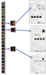
Paul explained that the Cornami TruStream computational fabric is like this. It is composed of basic building blocks called FracTLcores. Each core has a wrapper, memory and a reconfigurable core. These blocks are self-similar at each level of hierarchy and are connected by a very unique network on chip (NOC). These configurable processing elements can be assembled in many ways to solve specific problems, including running FHE in real time. Below is an example of 16 FracTLcores that are configured to implement a 64-bit RISC-V core. Some of the secret sauce here is that this type of configuration has no speed degradation and FracTLcores can be configured to optimally solve specific computational problems. If you need more speed, just add more FracTLcores.
Paul explained that each FracTLcore can execute seven decisions per clock cycle, and multiple chips can be assembled to solve larger problems with no performance degradation. The current estimates suggest running FHE in real time will require a 1,000,000X speedup. Paul explained that Cornami can deliver that.
The Future
So there is a glimpse into the future. It should be noted that not only can the Cornami TruStream computational fabric run FHE in real time, it can also secure the model and training data for all kinds of AI algorithms and run those algorithms at speeds that are unattainable today. These are indeed bold statements and I’ve only scratched the surface regarding the details behind how all this works.
You can learn more on the Cornami website. I can also recommend an insightful interview Dan Nenni did with Wally Rhines, who happens to be the president and CEO of Cornami. Without a doubt, Cornami’s TruStream computational fabric changes computing. Now you’ve all seen the future. I’ll leave you with a quote on one of Paul’s last slides.
Secure the data – Not the data center
Also read:
Conquering the Impossible with Aspiration and Attitude
CEO Interview: Wally Rhines of Cornami
Podcast EP65: Trust But Verify – The Backstory of Applied Materials and Cornami with Wally Rhines