RVN! 26 Banner revised (800 x 100 px) (600 x 100 px)

HFSS – A History of Electromagnetic Simulation Innovation

HFSS – A History of Electromagnetic Simulation Innovation
by Daniel Nenni on 01-14-2021 at 10:00 am

ansys HFSS electric field distribution in coax to waveguide adapter

In the 155 years since James Clerk Maxwell introduced the world to Maxwell’s Equations in the “Dynamic Theory of the Electromagnetic Field” there have been some amazing breakthroughs and avenues of insight. As a young electrical engineering student, we are introduced to the set of equations describing electromagnetic waves, but it is often difficult to visualize and understand wave propagation and how it pertains to high-speed electronic designs. It is in this area that Ansys HFSS stands out as the pioneer in this industry.

From the time that HFSS was introduced in 1990, it has provided a unique type of insight into electromagnetic problems. Diagnosing design issues in a lab requires measurement of time domain waveforms or S-parameters on components and test boards. Often, there are observations of these waveforms that defy basic understanding of electromagnetic phenomenon. From TDR (Time Domain Reflectometry) “glitches” or mysterious “suck-outs” in frequency domain S-parameters, debugging these designs can be extremely challenging. Modeling these structures in all their 3D complexity in a full-wave electromagnetic solver like HFSS can very quickly uncover the source of these problems.  The ability to excite a problem with real-world signals, watch the field propagate through the model, and quickly uncover hidden discontinuities or coupling mechanisms is invaluable.

On the capacity front of electromagnetic simulation, HFSS has been an industry leader. Engineers have always wanted to simulate ever larger and more complex designs. From the early days of HFSS with the solution of the coax-to-waveguide adapter shown in the image, designers have clamored for the ability to include larger 3D models, more detailed mechanical and electrical CAD, as well as more complicated material properties.  When HFSS was introduced, a then complex coax-to-waveguide adapter took approximately 10,000 matrix elements and 10 hours to solve just a single frequency point.  That same model today solves an entire band of frequencies in under 30 seconds on a laptop. The original full-wave FEM solution has grown from solving simple waveguide components to entire microwave systems, complex antenna arrays, and entire printed circuit boards.

There are many algorithmic innovations leading to the unprecedented scale users can solve in HFSS today. We have tackled problems such as multi-processing matrix solutions to distributing these solutions across dozens of compute nodes and hundreds of cores. HFSS introduced the first commercially available Domain Decomposition Method solver for full-wave electromagnetics leading to the ability to mesh and solve pieces of a large problem, then bringing them together for a full model field solution. Whether it is creating, developing, and commercializing new computational electromagnetic algorithms or more efficiently storing information, these enhancements have exponentially increased the speed and capacity of HFSS over the years. One recent example of large-scale IC simulation in HFSS can be seen here.

Some would claim that the increase in capacity is largely due to hardware innovation over the thirty-year history of HFSS. These hardware improvements, described in 1964 by Gordon Moore, and colloquially known as Moore’s law, have magnified these algorithmic developments. Floating point operations have improved in speed by almost 500 times since HFSS was first introduced. Combining the raw clock speed improvements of CPUs with the increased size and speed of cache and main memory, larger simulations can be performed in less time.

It is not much of a stretch to state that engineers have very little patience to wait for simulations. In my experience, the happiest engineer would be one who could solve an entire complex electromagnetic system within seconds from the comfort of their living room on their tablet. For some, the reality of working from home has been realized recently, but we are still not to the point of being able to solve these systems in seconds. However, using the Ansys Cloud and HFSS, these simulations can be accessed and monitored from the comfort of your phone or tablet.

Ansys Distinguished Engineer, Dr. Larry Williams notes that “the numerous electromagnetic method innovations in Ansys HFSS have enabled solutions that now propel the 5G, RF, Wireless, and high-speed industries.” To find out more about the innovations in the HFSS solvers and the history of our HPC computing advancements, take a look at these videos:

https://www.youtube.com/watch?v=N7v4fgDyxB4&list=PLQMtm0_chcLx5STq8Q_p1m79PyjkylvR8&index=3

https://www.youtube.com/watch?v=DC-SA4hloHQ&list=PLQMtm0_chcLx5STq8Q_p1m79PyjkylvR8&index=6

Also Read

HFSS Performance for “Almost Free”

The History and Significance of Power Optimization, According to Jim Hogan

The Gold Standard for Electromagnetic Analysis


Developing Drivers For The Automotive Industry

Developing Drivers For The Automotive Industry
by Daniel Nenni on 01-14-2021 at 6:00 am

mcal

Autonomous driving, connected vehicles, power electronics, infotainment and shared mobility are some of the developments which have mobilized the revolution within the automotive industry in recent years. Combined, they are not only disrupting the automotive value chain and impacting all stakeholders involved but are a significant driver in the growth of the automotive software market which is expected to cross $450 billion by 2030. Unfortunately, these rapid changes are making it difficult for automotive OEMs and other industry stakeholders to keep pace. This is partly due to the fact that a large part of these automotive innovations depends more on software quality, execution, and integration as opposed to mechanical ingenuity.

Despite the importance of software in the cars of today, the development of the embedded software modules is often either done in isolation, partnerships or sometimes bought from suppliers. These modules are then stitched together into a proprietary platform. But these proprietary platforms are difficult to support as the hardware supplied needs to work seamlessly with the platforms.

To ensure configurability, flexibility and maintenance for the hardware defined cars of today, there is a growing need for standardization of software defined transportation platforms. With the increasing complexity of hardware and software, it also becomes necessary to find common solutions across product lines. The Automotive Open System Architecture (AUTOSAR) is a big step in this direction and founded by companies such as Toyota, BMW, VW, Ford, Daimler and GM with the aim of standardizing the software architecture for the automotive industry. AUTOSAR enables hardware and software development to be independent of each other and makes it easier to implement the growing complexity, quality and reliability of the electronic systems used in the automobiles. This standardization has helped the automotive embedded developers in focusing primarily on the innovations in the product feature development rather than working on different architectures making it easier to reuse applications between ECUs. The open source AUTOSAR architecture has been adopted by several companies who in turn have given it their own flavor. These include companies like Vector, Elektrobit, Bosch etc. to name a few.

To provide flexibility to software developers, AUTOSAR has been developed using a layered approach to software development with the complete software split into multiple layers such as Application layer, Runtime environment and the Basic software. The Basic layer in turn has further been broken into the Services layer, the ECU Abstraction layer and the Microcontroller Abstraction Layer (MCAL).

The device drivers for the MCU are developed using the standard as specified in the Microcontroller Abstraction Layer which provides inputs to the software developer about the name of the API, the parameters of the said APIs and the overall functionality of the driver. The primary benefit of standardizing the APIs is that the MCAL drivers which have been developed can be reused across multiple customer projects by the OEMs as well as across multiple Basic Software Layers (BSWs) provided by multiple vendors. This results in reduced development times for the OEM as well as less integration efforts on the part of the SW Integrator. Consequently this leads to reduced time to market resulting in huge cost reductions for the OEMs.

How are MCAL device drivers any different?

In the automotive industry, there is a general understanding that the suppliers will supply the MCAL layer to be placed on the register level of the microcontroller. While reference implementation of MCAL may be provided by some suppliers, there is a big chasm which needs to be crossed in order to develop a production ready implementation. One of the major challenges faced while developing the device drivers is the rather complex interaction between specifically implemented hardware features and standardized software requirements. The device driver solutions also need to map the different software modules to the same microcontroller resource and need to manage the complex dependency between software driver configurations.

Moreover, anyone who has developed drivers or used a driver knows that the driver comprises of APIs which take certain parameters as defined by the driver developer. The application developer uses the developed APIs when developing applications to achieve a pre-defined functionality. While this is true in the case of AUTOSAR as well, and most of the APIs accept parameters which are passed by the application developer, there is another side to the AUTOSAR development process which deals with configuration of the MCAL.

The configuration of the MCAL is done using a Module Configuration Generator (MCG) which generates a configuration which is then given to the driver for it to configure the hardware as mandated during the configuration process. The configuration can then be used across multiple hardware platforms for the same microcontroller.

MCAL also requires an adherence to strict quality standards and considerations and defines how the drivers should be written. They have to be MISRA compliant and meet the necessary safety requirements (ISO26262). These include for example when to clear the allocated memory or ensuring parameters are not passed using pointers to ensure safety critical programming.

The development of the MCAL for different ASIL levels also possesses its own challenges. ISO26262 specifies particular processes and methodologies to be followed during the development of the MCAL drivers for different ASIL levels which often end up modifying the architecture of the MCAL driver. Some of the design changes to the MCAL driver can potentially include

  • The number of safety checks done in the driver. These include aspects such as monitoring of errors during register accesses, monitoring memory corruption, addition of safety markers to the configuration data etc.
  • Implementation of safety mechanisms needed in the event of errors during register accesses.
  • Memory partitioning has to be done such that variables of an ASIL-D driver (highest level of ASIL) do not occupy the same memory space or overlap as the variables of an ASIL-A driver (lowest ASIL level). This partitioning is done during system and software design.

Complex drivers

The complex device drivers are also a part of the AUTOSAR architecture and includes developing and integrating a driver, which does not need to conform to the AUTOSAR standard, into the BSW. As such the developer is free to architect their own driver with the APIs, parameters and functionality for the APIs according to their choice. But developing a complex driver is easier said than done as complex driver implementation often requires awareness of overall system constraints such as timing and latency requirements.

Our expertise

Vayavya Labs, with its considerable experience in the embedded domain, AUTOSAR and MCUs, provides an avenue for design companies to leverage their expertise for custom driver and software development for the automotive industry. It has successfully implemented MCALs for multiple hardware platforms across multiple OEMs such as Synopsys’s ARC HS3x and EM6 processors, Calterah’s Alps 77GHz Radar SoC, NXP’s MPC5748 controller to name a few. It has also developed MISRA compliant drivers for Spi, Qspi, Ethernet, Can, Can-FD, Mcu, Port, Dio, Pwm, Gpt, Adc modules.

Vayavya Labs also provides a software platform – DDGEN – to automatically generate MISRA compliant device drivers for commonly used peripherals to ensure rapid development of automotive applications.

 Also Read:

CEO Interview: R.K. Patil of Vayavya Labs

A Blanche DuBois Approach Won’t Resolve Traffic Trouble

Chip Shortage Killed the Radio in the Car


2020 was a Mess for Intel

2020 was a Mess for Intel
by Robert Maire on 01-13-2021 at 10:00 am

Intel 2020 Mess

Understanding Intel’s future means understanding Intel’s past

Yes, there are two paths you can go by, but in the long run. There’s still time to change the road you’re on.

Intel is at a crossroad. The road they have been on since inception, and the road that has differentiated them from the rest of the pack and made them great was their manufacturing prowess. They are the last “real man” standing that owns their own fabs.

Now we are at a point where Intel has to decide whether to continue to try to be the last CPU IDM, patch up their mistakes and stumbles in manufacturing and recover their greatness (although maybe not Moore’s Law leadership). Or, throw in the towel and follow AMD and everyone else into TSMC’s warm embrace. Or perhaps some half baked compromise between the two extremes.

There is no easy way out nor clear decision to be had. And you may ask yourself, “Well, how did I get here?”

AMD was taking their last dying gasps, Apple gave up on PowerPC and went all in with Intel. Intel was flying higher, even more so than its partner Microsoft.

Then a few years ago, it seemed as if something started happening and it all started unraveling.

It was not a single point in time nor was there a single inflection point event that signaled a change in Intel, it came about much more slowly, much more insidiously.

Lets get rid of our most experienced people

A few years ago, back in 2016, Intel did a “RIF” (reduction in force) of about 11%. Intel had previously done a significant reduction way back in 2006 of about 10%. At the time we noted that Intel seemed to be trying to soften the blow by offering early retirement and other “packages” to older employees with the most seniority (and experience). It seemed to us , as a casual observer, with some friends at Intel, that the RIF had gone well beyond its original intent and Intel was losing real, experienced, talent, who were taking the attractive “package” and leaving pre-maturely without transition.

In an industry that runs on “tribal knowledge” and “copy exact” and experience of how to run a very, very complex multi billion dollar fab, much of the most experienced, best talent walked out the doors at Intel’s behest, with years of knowledge in their collective heads

Lets go buy some stuff with the money burning a hole in our pockets

Intel over the past years has also been on a bit of a shopping spree, buying all nature of companies for very high valuations. Though we won’t go through all the acquisitions, they all seemed to have some sort of legitimate justification or logic even though they may or may not have exactly been anywhere near Intel’s wheelhouse. In the end , when we add up the price of the acquisitions and try to calculate the value added to Intel we come up very short.

While we would never criticize M&A as a method to grow as we think that properly applied acquisitions can propel a company well beyond its peers and into new, faster markets, badly done M&A, done with weak logic, can sink a company.

Mobile Phones are toys that will never amount to anything

Intel famously balked at making CPUs for Apple’s Iphone and essentially completely “whiffed” on the smart phone and tablet markets while TSMC embraced it. (This somehow reminds me of a software analyst I knew when we both were at Morgan Stanley, telling Bill Gates that microcomputers wouldn’t amount to anything when Morgan was pitching for Microsofts IPO business, which Goldman got and put them on the tech map). Though this was a single, key mistake, there was never a significant recovery effort until the game was already over.

Forgetting your roots/ Taking your eye off the ball

Perhaps the peak of my concerns about Intel came a number of years ago at an Intel event. The CEO of Intel at the time (name withheld to protect the innocent…) was doing a presentation about all the myriad of new markets that Intel’s was getting into and looking at.

It was a litany of multi billion dollar opportunities and amazing technologies. He spoke for an hour on a host of topics and I never heard him use the word “semiconductor” (or chip) once. You would not have known from the speech that Intel was even in the semiconductor business in any way, let alone that it was the “leader” from which all its profits came. When I walked out of the room I had the urge to short Intel on the spot….but didn’t.

Deserting a sinking ship

When we heard that the legendary Jim Keller was leaving Intel in the beginning of 2020 it was clearly an ominous sign. Jim is the semiconductor design genius/guru that has had stints at Tesla, Apple, AMD and finally Intel. He has been a bit of a turn-around/seal team that parachutes in for a few years, pulls off a miracle and then hops on to the next lily pad to come to the next companies rescue. He has since moved on to an AI chip start up that he will lead.

His departure around the time that Apple also abandoned the Intel ship was a very clear indication that things were already sinking. Here we are, almost a year later still without a rescue plan.

A plane crash is never “just one thing” went wrong

My point in all this is that Intel’s problem is not just bad yields and delays of 10NM and 7NM caused by a singular or some number of esoteric technology issues that caused them to fall behind TSMC in Moore’s Law.

Sure, that’s the manifestation of other underlying issues that taken together have caused those symptoms to come to a head to cause problems. Its a bit like an airline trying to decide whether to outsource its airplane maintenance after a plane crashed due to a loose screw after years of neglect, mistakes and laying off the most experienced mechanics. Maybe its not the mechanics faults.

Maybe its a managerial fault that needs fixing first. For inspiration look at what the semiconductor winners are doing

It is interesting to note that Intel used to be the biggest spender on capex in the industry and was passed by around the time of its issues starting to manifest by both TSMC and Samsung.

We are now looking ay Samsung potentially spending a record $30B a year and TSMC spending a record $20B, both more than Intel.

While randomly throwing money at an issue is not a solution, a focused spend on both machinery and people that are key to your leadership position is well warranted and should not be subject to cuts to come in on budget or make a quarterly earning number. It is clear that TSMC, Samsung and now the Chinese, view long term spend and commitment in semiconductors as crucial to long term success despite short term impact. Focusing on the stock price, buybacks and acquisitions while using capex and R&D to balance the budget is the quintessential sacrificing long term for short term.

The problem is much bigger than just Intel

While we love Intel as being an American technology pioneer and former leader, we are also worried about Intel being the last standing US semiconductor maker (not counting Micron…which doesn’t quite count). As we have written about extensively for many years, the risk to the greater US, its national defense and economy by losing semiconductor leadership is well beyond what most people can even begin to understand.

The numbers are many times Intel’s revenues and go well beyond just dollars and cents to national security.

While Intel and its shareholders are not responsible for the US national economy and security, the alignment between Intel’s long term success and the US’s best interest is clear and synergistic.

AMD’s example is not a good one

Many investors and analysts would take the easy position that following AMD’s lead in splitting the company in two between the fabs and the rest of the company worked for AMD and will work for Intel. We think that this is not a good comparison.

AMD did not have the minimum critical mass needed to support a fab and all the R&D that goes along with it. Intel has the size, scope and market needed to support the associated spend. The basis of the problem is not economic as it was with AMD it is an execution/technical problem that Intel has encountered. The divorce between AMD and its fab did not work out too good for its fab (now Global Foundries).

AMD did find a buyer (sucker) in Abu Dhabi, who thought they were going to buy their way into high tech but didn’t anticipate the years and billions of endless spending to keep up in semiconductors, especially without the requisite revenue/profitability to support it. The math simply didn’t work and they wound up bailing out of the Moore’s Law race. GloFo is now off hiding in a “specialized” corner of the semiconductor industry hoping to avoid being trampled by the bigger players before they can IPO or otherwise unload the company.

Investors will point to AMD’s recent success but we would point out that that success is more of an example of TSMC’s success than AMD’s, much as Apple’s success is directly linked to TSMC and Nvidia and others etc;. While we take nothing away from Lisa Su’s management of AMD, she did have the luck of being in charge when the supply deal with the millstone that was GloFo expired and AMD was free to use TSMC as a fab, which was somewhat of a “no-brainer” . Intel does not have the luxury of the same luck nor easy decision to make.

Intel’s situation is much more complicated. In addition, AMD honestly didn’t have much of a choice at the time.

Putting toothpaste back in the tube is not easy

The other end of the decision spectrum is doubling down and fixing the existing issues with Intel’s manufacturing problems. Regaining leadership in Moore’s Law is likely a lost cause that can’t be recovered as we haven’t seen TSMC ever stumble which is likely what Intel would need to happen.

We are also at a bit of a transition as Moore’s Law is indeed slowing and becoming more difficult and multiple cores, multiple packaged die, 3D stacking and other alternatives attempt to make up for the geometric slowing.

This means that it isn’t just catching up to TSMC on Moore’s Law by leapfrogging a generation or miraculously fixing the yield issues it also means doing a lot on the many alternative technology fronts. Intel does have the resources to fight a multi-front war. It would mean a likely increase in spend and duplicate costs as Intel would have to outsource to TSMC while at the same time also spending to fix and improve their existing process and technologies.

This larger incremental cost would likely not sit well with investors as the additional costs would squeeze profitability in the short run (likely a number of years)

Outsourcing only works if you have multiple potential manufacturers…

We would point out that outsourcing only works in the long run if you have multiple, equally competent outsource partners to play off one another to keep them honest and pricing reasonable. If both Intel and AMD outsource to TSMC without Samsung as a viable alternative, they will both lose as TSMC will be in the drivers seat and will be able to determine winners and losers and pricing. AMD being at TSMC has worked because the real competition has been TSMC versus Intel.

We would also point out that Apple is an even more vulnerable position than Intel with TSMC now that it has decided to move all its laptop/desktop CPU business away from Intel and put all its eggs in TSMC’s basket. In Apple’s case they have even less alternative as going to Samsung foundry as a backup/alternative/ stalking horse against TSMC is not a very viable alternative. Apple is perhaps even more vulnerable than Intel would be.
Even though Samsung is pouring oodles of money into its hugely profitable chip business it doesn’t mean they will be competitive in foundry and where they are making money is memory anyway.

Outsourcing is a “burn the boats”/”roach motel”, one way decision that there is no recovery from if it doesn’t work and it will likely put Intel at the mercy of others. Both Intel and AMD will be in the exact same boat.

Thinking outside the box

We would imagine that there should be alternative, unique solutions to Intel’s manufacturing issue.

Could Intel buy/rent TSMC’s process/know how? Could TSMC help fix/run Intels advanced fabs? Could Intel become TSMC’s presence in Arizona?

What alternative arrangements can get Intel’s manufacturing back on track more quickly while using TSMC in the interim as a fill in the gap in manufacturing?

Could the US government get involved with the “Chips for America? act as the threat of losing Intel’s manufacturing would be a clear case for that legislation.

Maybe Apple would be willing to chip some money in to get on shore manufacturing that is not dependent on an isolated island off of mainland China.

There should be a way to help Intel out in the near term with manufacturing and help TSMC out with presence and diversity outside of its island.

Maybe Samsung could step in as some white knight and team up with Intel such that both get a synergistic effect with their logic manufacturing efforts.
We think that this complex situation requires a complex, out of the box, solution which will require some compromise.

The Stocks

Unfortunately we don’t see an easy way out for Intel that doesn’t hurt either the short term or long term valuation. If Intel increases outsourcing and abandons being a fab leader they will sacrifice long term value for short term profits and a quick/easy fix.

If they choose to stay in the game, short term profits and the stock will be hurt by the extra expense of outsourcing while at the same time continuing to invest even more to fix the problem as an independent manufacturer.

If Intel chooses the outsource approach we would likely look to get out of the stock after it had run up on the news of the cost cutting and investors thinking the same thing will happen to Intel that happened to AMD.

If Intel chooses to fight on independently, we might be tempted to wait for a lower entry point as the impact on profitability would increase.

The wild card is some sort of in between solution that is a unique hybrid that is difficult to game out, but that may be the best hope for a good outcome.

From the perspective of semiconductor equipment makers, Intel giving up the ghost would be very bad as they would not only lose Intel’s spend but would have to deal with an ever more dominant TSMC that would take industry spending from 3 players down to two oppressive giants, Samsung and TSMC. More customers are always better for equipment makers.

Tokyo Electron & Hitachi does a lot of Intel business as does KLA and to a slightly lesser extent Applied. Lam is more exposed to Samsung. ASML already does the vast majority of its business with TSMC and less with Intel so they would see less impact.

About Semiconductor Advisors LLC
Semiconductor Advisors is an RIA (a Registered Investment Advisor),
specializing in technology companies with particular emphasis on semiconductor and semiconductor equipment companies. We have been covering the space longer and been involved with more transactions than any other financial professional in the space. We provide research, consulting and advisory services on strategic and financial matters to both industry participants as well as investors. We offer expert, intelligent, balanced research and advice. Our opinions are very direct and honest and offer an unbiased view as compared to other sources.

Also Read:

SMIC Blacklist puts ASML in Jam

Noose tightens on SMIC- Dead Fab Walking?

China Semiconductor Bond Bust!


CDC, Low Power Verification. Mentor and Cypress Perspective

CDC, Low Power Verification. Mentor and Cypress Perspective
by Bernard Murphy on 01-13-2021 at 6:00 am

CDC Low Power

Clock domain crossing (CDC) analysis is unavoidable in any modern SoC design and is challenging enough to verify in its own right. CDC plus low power management adds more excitement to your verification task. I wrote on this topic for another solution provider last year. This time I want to intro an interesting twist on the problem, revealed in a Mentor/Cypress white paper presented at DVCon San Jose last year.

Scoping down CDC analysis reduces noise, so Mentor and Cypress focused their attention on interactions between low power and CDC. Obvious candidates are around isolation management and retention registers. Since they’re working with RTL design which does not yet have power management implemented, they read the current UPF (power management constraints) together with the RTL.

CDC and isolation control

One obvious CDC+low power problem, illustrated in the figure, would not necessarily be obvious in a CDC analysis of the RTL alone where the isolation signal is not yet connected. In this case there is a clock domain crossing between clk2 and clk1, which could lead to metastability in the B2 register when isolation is enabled (or, I think, when it is disabled). Which means you must harden B2 for metastability, or you must synchronize the isolation enable signal. Either way this is a realization that only becomes apparent when you look at the RTL and the UPF together.

CDC and retention

Retention registers provide another tricky example. In RTL a register is just a register – no power considerations of any kind. If you power off the block containing the register, the register powers off along with everything else in the block. But that can introduce a lot of latency and rework when you want to power back on. When your phone automatically powers down and a little later you start it up again, you don’t want to have to restart all your apps and re-find the last things you were looking at. You expect the phone to jump right back to where you left off. Retention registers play a role here. These registers hang on to their last state, even when you power down the domain around them. Not every register has to be retention, just enough to allow jumping back quickly to the last state when power is restored. To my knowledge, this typically works by saving state to a separate part of a special register, where that separate part sits in an always-on power domain. When you’re ready to restore, you copy that saved state back to the main register.

The CDC challenge again starts with the fact that designer flag these decisions in the UPF, not in the RTL. And choose signals to trigger state restoration which must be synchronized to the register clock. This is another case where a check has to look both at the RTL and the UPF. First to find the retention candidates and then to ensure that no restore signal has a CDC issue with its target register.

Mentor solution

Interesting stuff. I wonder if at some point we will be seeing white papers on CDC and security verification. Or maybe CDC and low power and security! You can access the Mentor white paper HERE.

Also Read:

Multicore System-on-Chip (SoC) – Now What?

Smoother MATLAB to HLS Flow

A Fast Checking Methodology for Power/Ground Shorts


ESD Alliance Report for Q3 2020 Presents an Upbeat Snapshot That is Up and to the Right

ESD Alliance Report for Q3 2020 Presents an Upbeat Snapshot That is Up and to the Right
by Mike Gianfagna on 01-12-2021 at 10:00 am

ESD Alliance Report for Q3 2020 Presents an Upbeat Snapshot That is Up and to the Right

The Electronic System Design (ESD) Alliance (a SEMI Technology Community) recently released their regular report on EDA revenue for Q3, 2020 . While the report is a normal occurrence, the numbers in this particular report are anything but normal. I have been reviewing these reports for many years, and I honestly can’t remember a more positive result. There have been plenty of things to remember from 2020 that evoke sadness. If you care about the EDA industry, take heart. There is something to be happy about. Read on to see how the ESD Alliance report for Q3 2020 presents an upbeat snapshot that is up and to the right.

Let’s start with some of the basics. EDA revenue increased 15 percent in Q3 2020 to $2,953.9 million, compared to $2,567.7 million in Q3 2019, with all categories logging significant gains. The four-quarter moving average, which compares the most recent four quarters to the prior four quarters, rose by 8.3 percent. The companies tracked in the report employed 47,087 people in Q3 2020, a 4.8 percent increase over the Q3 2019 headcount of 44,950 and up 1.1 percent compared to Q2 2020. Substantial revenue growth and higher employment. Happy days are here again. Before I got too gleeful, I wanted to get some more detail – the story behind the numbers. For that, I was fortunate to be able to spend some time with Wally Rhines, Executive Sponsor, SEMI EDA Market Statistics Service.

Wally always seems to have a substantial amount of detailed information and broad perspective at his fingertips. This discussion was no different. Wally started by explaining there have been three times in the past 15 years when EDA growth has reached 15 percent. So, this is about as good as it gets for recent EDA history. Wally pointed out that perhaps you could see a weakness in services revenue, but that’s about it. We talked about that category a bit. Services revenue is defined as support for tool deployment, training and design work. Looking at support and training for tool deployment a positive story can be seen in the numbers, however. EDA tool flows are becoming more user driven. The result of that is a reduction in the need for expert AE support and training, so a reduction in services can signal a good trend.

Looking at the bigger picture, Wally explained that the semiconductor industry will likely grow five to six percent this year. He went on to explain that EDA typically grows one point more than semiconductor. In the last three years, EDA has been growing about four points faster. EDA is exhibiting accelerating momentum. More good news. IP is another bright spot. As a newer market category for EDA, growth has been large, almost 26 percent year on year. IP is now about 35 percent of the total EDA revenue number.

Another somewhat counter-intuitive aspect to the numbers is the impact of consolidation. M&A activity typically brings synergy to the merged company, resulting in lower EDA spend. Yet we’re seeing a healthy increase. The impact of all the new players, think Google, Amazon, Facebook and other system companies like that are neutralizing the consolidation effect. As Wally pointed out, in spite of M&A and the associated headcount reduction, designers are still designers. They find opportunity somewhere else, and thanks to the trend for system design companies to bring semiconductor design in house, design folks find a good job market.

Overall, a very positive story for EDA and semiconductors in the face of a challenging year. It was very helpful to get some of the backstory from Wally about how the ESD Alliance report for Q3 2020 presents an upbeat snapshot that is up and to the right.


The Latest in Dielectrics for Advanced Process Nodes

The Latest in Dielectrics for Advanced Process Nodes
by Tom Dillinger on 01-12-2021 at 6:00 am

new ILDs v2

Of the three types of materials used in microelectronics – i.e., semiconductors, metals, and dielectrics – the first two often get the most attention.  Yet, there is a pressing need for a rich variety of dielectric materials in device fabrication and interconnect isolation to satisfy the performance, power, and reliability constraints of current microelectronic products.  Indeed, advances in dielectrics have been at the heart of the continued scaling achieved in advanced nodes.  (High-k gate dielectrics, for example.)

Additionally, the chemical properties of dielectric materials are critical in many process steps, from their use as a patterned hard mask to serve as a protective etch barrier to their use as a sidewall spacer to enable selective epitaxial growth on exposed silicon.  Dielectric materials need to support a multitude of deposition techniques, from chemical vapor deposition for isotropic addition on the surface topography to spin-on dielectric coatings to fill trenches.

Research in new dielectric materials is crucial, to support aggressive power, performance, yield, and reliability targets.  At the recent IEDM conference, Intel presented two papers describing some of their research (and other contributions) into the introduction of new dielectrics, and an interesting approach toward the corresponding metal interconnect fabrication.  [1, 2]  This article summarizes the highlights of these presentations.

Background

As briefly mentioned above, dielectrics are required to satisfy a multitude of requirements:

  • device gate oxide

Traditional Dennard scaling of the SiO2 gate oxide tox, with dielectric constant k~3.9-4.0, reached a non-manufacturable limit over a decade ago.   (For each new process generation, the multiplier for tox is 1/S, where the scaling factor S>1.)

New high-k gate dielectrics were required, to maintain the gate-to-channel electric field, while ensuring a sufficiently thick oxide layer to be manufacturable – i.e., uniformity, low defect density, low leakage current, low trap density, high dielectric breakdown strength.  Common examples are SiON, HfO2, HfSiON, and Al2O3.

Devices in each new process are now quoted with an effective gate oxide thickness, using SiO2 as the reference:   k(high-k)/tox(high-k) = k(SiO2)/tox_effective.  For example, if the target scaled tox_effective ~3nm, a 16nm HfO2 gate oxide layer would be fabricated, helping to achieve the manufacturability goals listed above.

  • M-I-M capacitors

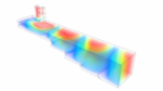
High-k dielectrics are also crucial to the fabrication of metal-insulator-metal (decoupling) capacitors in the back-end-of-line fabrication, as illustrated below. [3]

The goal is to provide a high capacitance per um**2 , with minimal impact to available global routing tracks.

  • interlayer dielectrics (ILDs) surrounding interconnects

In this case, low-k dielectric materials have been introduced to reduce the parasitic capacitance (and thus, the R*C time constant) of interconnects.  Prior to the mid-90s, deposited SiO2 was the prevalent ILD, subsequently replaced with alternative low-k oxides – e.g., carbon-doped oxides, such as SiCOH (aka, “Black Diamond”, a TM of Applied Materials). [4]

Ongoing R&D into these ILD materials has drive the dielectric constant to k~2.3, a marked improvement over SiO2.  Recently, air gap dielectrics (k=1, ideal) have been introduced into BEOL processing – more on air gaps shortly.

A concern is the structural integrity of these ILD materials, due to their greater porosity.  This is especially true for low-k ILDs at higher metal levels, due to the stress introduced by the thermal expansion differences between the silicon die, encapsulation material, and package – delamination issues of the BEOL metal layers is a known failure mechanism.

There are also (very thin layer) dielectrics needed in the metal stack to serve as copper diffusion barriers.  (The diffusivity of CU into high-porosity ILDs is high.)

  • etch stops/etch barriers

A hard mask dielectric is patterned on top of a material which is to be protected during a process etch step.  The HM needs to have a very low etch rate relative to the exposed material being removed.  In a subsequent etch step, the HM needs to have a very high etch rate to the surrounding materials (assuming the HM is not a “leave-behind” layer).

  • dielectric deposition

To date, the majority of dielectric deposition process steps provide an isotropic layer over the die surface topography, whether using a chemical vapor deposition or spin-on method.

In a self-aligned, double-patterning process, a subsequent anisotropic etch step is used to provide “sidewall spacers”, as illustrated in the figure below. [3]

These spacers offer a unique, controlled method for several key process steps:  definition of fins for FinFET devices;  adding a dielectric between gate and source/drain nodes (with the spacer serving as a HM for subsequent S/D epitaxial growth).

Recent research is focused on a novel selective deposition process, where dielectric materials are deposited on specific die surfaces only – more on this unique method shortly.

New ILDs

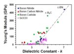
Intel reported results on alternative ILDs to the current SiCOH-based low-k materials, using boron carbides (BCH) and boron nitrides (BNH).  The figure below illustrates the dielectric constant versus Young’s Modulus for various ILD materials.  (Young’s Modulus, or the “Modulus of Elasticity”, is an indication of the deformity of a material when subjected to stress forces – a higher coefficient implies less deformation.)

Note that while the dielectric constant for SiCOH is indeed low, the material strength is poor – alternatives with comparable k and higher strength are attractive.

ILDs for Subtractive Etch Metals

There is also active research into alternative interconnect metals to Cu, specifically Ruthenium.  The prevalent method for fabricating Cu wires and vias uses the formation of dual damascene trenches, with initial barrier/seed layers prior to Cu deposition.  This is followed by chemical-mechanical polishing (CMP) for surface planarization.

The potential introduction of Ru as an interconnect metal has renewed interest in patterning using subtractive etch – a deposited metal layer is masked, then etched, as was the case for Aluminum wires used prior to the transition to Cu.  In this case, deposition of the ILD is done after metal patterning – a flowable dielectric is an attractive option for filling the (high-aspect ratio) volume between the wires.

Selective Dielectric Deposition

For advanced process nodes, as illustrated above, a self-aligned, dual patterning (SADP) step is pursued to enable an aggressive pitch of etched layers, as an alternative to the cost of multipatterning lithography/etch process sequences.  Clearly, a lot of process steps are required to implement SADP.

An attractive alternative would be to implement selective deposition of the dielectric material (e.g., as an etch barrier).  The Intel IEDM paper shared research results on a “bottom-up” area-selective atomic layer deposition approach.

The figure on the left below illustrates selective deposition processes of interest:  dielectric deposition on an exposed metal surface (capping layer), dielectric deposition for trench fill, and selective sidewall dielectric deposition.  The figure on the right shows dielectric deposition on an existing dielectric but not the adjacent metal.


The figure on the right illustrates an approach to selective deposition — the wafer is pre-treated with a material which preferentially forms self-assembled monolayers on a specific surface.  Subsequently, atomic layer deposition of the dielectric does not nucleate and grow on this pre-treated area.

One specific application of selective deposition is illustrated below.

The use of graphene as an (atomically-thin) capping layer for Cu interconnects has been shown to improve (reduce) Cu line resistivity, compared to current capping dielectrics.  (A 15% experimental reduction in Cu resistivity is shown — that’s a major improvement.)

There are challenges, to be sure – the deposition selectivity should be high and the defect density low.  Nevertheless, selective dielectric deposition holds great promise to reduce fabrication process complexity.

Air Gap Dielectrics

The optimum ILD dielectric constant is 1, associated with an air gap between interconnects.  Intel has previously described their process for fabrication of air gaps, as illustrated below. [5]  After (damascene) metal patterning, the dielectric between the metal lines is etched, a thin diffusion barrier is added, and the next layer ILD is deposited and planarized.

An example of the delay/energy benefits of air gap dielectrics is shown below – the (simulated) circuit example is a datapath multiplier.

Dual Metal Layer Thickness

At IEDM, Intel also presented results from R&D efforts to provide two metal line thicknesses for an interconnect layer.

This option allows unique selection of line R and C values that comprise the R*C time constant, for optimal “tuning” of wire delays.  A first-order Elmore delay model for an RC interconnect tree is illustrated below, with the resulting effective point-to-point R*C summation equation. [3]  Note the strong dependence of the delay on the initial wire R values.  A dual-metal thickness option would offer unique R and C combinations along the fanout paths.

The process flow for fabrication of metal thicknesses  a-only, b-only, a+b, and vias is depicted graphically and with TEMs in the figures below.  (The option for fabricating air gaps between the two metal thicknesses is also shown.)

Layer ‘a’ and the vias utilize a dual-damascene process flow, while layer ‘b’ is single-damascene, followed by CMP.  Note the depth and aspect ratio of the air gap is quite high, to minimize the coupling capacitance values between adjacent wires, regardless of their thickness.

The figures below illustrate calculated values and testsite measurements for Cwire and R*C time constant for various interconnect thickness configurations:   all b;  all a+b;  b alternating with a+b;  a+b alternating with b;  with and without air gap dielectrics.

(Note that there is still the requirement to model the wire thickness tolerances due to CMP removal variation due to local interconnect density ranges.)

An example from Intel where separate R and C optimizations might be useful is shown below.

For a register file, the R*C delay product is more impactful for the address decode and word-line drivers (in M4 and M3), whereas C optimization may be the focus for (local and global M2) bitline implementations.

Summary

The demands on dielectric materials are great, from low-k ILDs to high-k gate oxides.  Hard mask etch stops require differentiated etch chemistry to surrounding layers.  New selective dielectric deposition methods offer the potential for significant process cost savings.

Although perhaps less captivating than new semiconductor and metallization materials being pursued, investigations into improved dielectrics is crucial to the PPA, yield, and reliability roadmap for microelectronics.  At IEDM, Intel provided an update on the activity that they and other researchers are pursuing.  I would encourage you to review their presentations.

-chipguy


References

[1]  King, S., et al, “A Selectively Colorful yet Chilly Perspective on the Highs and Lows of Dielectric Materials for CMOS Nanoelectronics”, IEDM 2020, Paper 40.1

[2]  Lin, Kevin, et al, “Staggered Metallization with Air gaps for Independently Tuned Interconnect Resistance and Capacitance”, IEDM 2020, paper 32.5.

[3]  Dillinger, T., VLSI Design Methodology Development, Prentice-Hall, 2019.

[4]  https://svmi.com/service/low-k-films/

[5]  Fischer, K., et al, “Low-k interconnect stack with multi-layer air gap and tri-metal-insulator-metal capacitors for 14nm high volume manufacturing”, IEEE Intl. Interconnect Technology Conference, May, 2015.

[6]  Hashemi, F., et al, “Selective Deposition of Dielectrics:  Limits and Advantages of Alkanethiol Blocking Agents on Metal-Dielectric Patterns”, ACS Applied Materials and Interfaces, Nov 2016.


Achronix Speedster7t Garners Best Practices Award for FPGA

Achronix Speedster7t Garners Best Practices Award for FPGA
by Tom Simon on 01-11-2021 at 10:00 am

Frost and Sullivan 2020 Award Achronix

FPGAs have played an important role in the growth of key markets, including networking, storage, mobile devices, etc. They offer a unique set of capabilities that ASICs, CPUs and GPUs find hard to match. FPGAs are wire-speed, programmable integrated circuits that accelerate data and applications.  The ability to reprogram the devices, even once they are deployed in an application, provides optimal flexibility while still yielding best-in-class performance efficiencies.  Some of the leading applications in these fast-changing markets include AI/ML for data center, edge compute, Industry 4.0 and intelligence for automotive, video compression, storage- and network-based acceleration, security and virtualization.  FPGAs are poised to be instrumental in the successful deployment of these applications.  Achronix Speedster7t provides the fastest interfaces in the market for an FPGA with PCI-e Gen 5, 400GbE and GDDR6.  Connecting all of the internal functional blocks, like machine learning processors (MLP),

general purpose DSPs, FPGA fabric as well as the external I/O is Achronix’s groundbreaking network on chip (NoC) which exceeds 20Tbps of bi-directional bandwidth.   Unlike other FPGA vendors, Achronix goes one step further and provides its technology as IP for integration into custom ASICs.   With this in mind the industry research firm of Frost & Sullivan has looked at the players in the FPGA market and has awarded Achronix with their 2020 Best Practices Award for FPGA for the Data Center Industry.

Achronix Speedster7t Award

Frost & Sullivan has a well-defined methodology for assessing companies and their technology for their level of innovation. The Frost & Sullivan best practices research paper on Achronix outlines the criteria and process for this assessment. It comes down to more than just what is in the product; it includes how the company works with customers and the internal processes to ensure the best results. Frost & Sullivan breaks it down into two main areas, New Product Attributes and Customer Impact.

New Product Attributes includes matching customer needs, reliability, quality, positioning and design. Customer Impact covers price/performance value, customer purchase experience, customer ownership experience, customer service experience and brand equity. Frost & Sullivan has in-house expertise and also uses external industry experts to vet their rankings.

Achronix scored high because of many factors. The Frost & Sullivan paper provides background on the growth of Achronix and a summary of Achronix’s Speedster7t architecture. Achronix offers both discrete FPGA devices and  embedded FPGA (eFPGA) intellectual property used for the development of custom ASICs and/or chiplets.   Achronix offers a 2D network on chip (NoC) that frees up the FPGA fabric resources by providing point to point high speed data transfers within the FPGA fabric and to memory, network and serial interfaces. Speedster7t also comes with PCIe Gen5, 400Gb Ethernet and GDDR6 interfaces for high speed data operations. Frost & Sullivan  highlights the dedicated arithmetic units in the FPGA fabric that support AI/ML operations. These Machine Learning Processors (MLP) are useful for programming the massively parallel operations that are needed in AI/ML processing.

Frost & Sullivan also looked at corporate culture and processes to rank Achronix. All of the peripheral interfaces undergo rigorous qualification prior to inclusion in their products. They have adopted state of the art IP that offers the highest performance and quality. Achronix also has built their development environment using industry standard tools. This means that new customers will already be familiar with the flow. Achronix has also pioneered 24/7 support through an online support system that makes it easy for customers to get any needed answers.

Achronix partners with customers, sharing their product roadmap to get early feedback. Also, eFPGA customers get expert help on configuring resources to ensure their applications will work optimally and integrate with the other SoC components. These steps help ensure first time silicon success and future-proofing so customer products will have long product lifetimes.

These fast changing markets like 5G, Automotive, Edge Compute and Data Center and their associated applications such as AI/ML, video compression and storage- and network-based acceleration, security and virtualization combine to make exciting opportunities for FPGA-based designs. Achronix has spent the time to deliver innovations that set them apart from the other players. Frost & Sullivan offers comparative rankings of several FPGA vendors in their report. The full report is available for download at the Achronix website. It offers a good overview of the FPGA market and interesting specifics about Achronix and the Achronix Speedster7t.


Webinar: Rescale is Providing an On-Ramp to the Hybrid Cloud for Chip Design

Webinar: Rescale is Providing an On-Ramp to the Hybrid Cloud for Chip Design
by Mike Gianfagna on 01-11-2021 at 6:00 am

Webinar Rescale is Providing an On Ramp to the Hybrid Cloud for Chip Design

We all know that design complexity is increasing at a fast pace. There’s always more analysis to run on larger and larger volumes of data. During tapeout, these demands can grow by an order of magnitude. Successful design projects need to add huge amounts of CPU, memory and storage for short bursts of time during tapeout to meet their schedule and time-to-market imperatives. All this wreaks havoc with the predictability and long-lead time provisioning associated with on-premises data center operations. “Bursting” to the cloud is the perfect answer to this difficult problem but getting there efficiently and reliably can be a complex task.  Until now. Recale has developed a comprehensive solution to this problem and they explain their approach in a very informative webinar. If you want to learn how Rescale is providing an on-ramp to the hybrid cloud for chip design, read on.

This webinar was originally presented as part of the SemiWiki Webinar Series and the replay is now available from Rescale. A link is coming, but first let’s examine what you’ll see and learn by attending. The webinar presents the benefits of a hybrid cloud approach to empower design teams to accelerate time to market and reduce schedule risk. Rescale’s all new hybrid cloud platform is presented. The platform is built to seamlessly transition workloads to the cloud for increased scale and performance, while maintaining the highest level of security and efficiency.  

Before I get into more details, I want to offer a personal perspective on the topic of cloud-based IC design. Simply put, it’s not as easy as it seems. During my time at eSilicon, we pioneered a complete cloud-based environment for front-to-back IC design. As they say, the devil is in the details and we encountered our share of demons along the way. Run-time consistency between on-prem and cloud, data coherency and controlled and efficient provisioning are just some of the challenges. A platform to handle all this is something to look at very seriously if you are contemplating a hybrid cloud environment.

Jose Fernandez

The webinar begins with Jose Fernandez, Semiconductor and Electronics Partnerships, providing an overview of Rescale. The company has been around since 2011 and has built an impressive portfolio of partners, customers and deployed applications. The figure below summarizes some of this data. Jose goes on to discuss the challenges of IC design today and the rather full platform Rescale provides to address these challenges. The names listed in this section will be familiar to all; Rescale has quite a large reach.

Rescale at a glance
Jeff Critten

Next, Jeff Critten, Account Executive discusses how Rescale’s capabilities impact chip design. Jeff provides details about how the platform is configured and highlights ease of use. The specific workflows supported are detailed. Jeff then presents several customer use cases and success stories. This discussion provides a lot of detail about what the problem was, who had it and how it was addressed. There is a well-produced video embedded in the webinar from Gaon Chips about how they use Rescale and the hybrid cloud to address their design challenges. This video alone is worth the time to view the webinar. You’ll hear perspectives from employees and ecosystem partners.

Riaz Liyakath

Next, Riaz Liyakata, Solutions Architect takes you through a Mentor Calibre live demo. Before he gets into the Calibre DRC demo on the cloud, Riaz provides an overview of the EDA tools and cloud providers that are available on the Rescale platform. The list is very complete and very impressive. The Calibre demo covers all aspects of deploying a complex application in the cloud, including provisioning, data management and runtime support. This is a very complete demo and will give you a strong sense of the breadth of the Rescale platform.

Jose completes the webinar with a summary of Rescale’s core strengths and benefits. I don’t want to give too much of the webinar content away, but this phrase says a lot:

Rescale is easy and powerful EDA in the cloud

If you are contemplating the need to burst to the cloud for your next design project, you need to see this webinar. Rescale is providing an on-ramp to the hybrid cloud for chip design. You can access the webinar replay here.


Car Wars 2021

Car Wars 2021
by Roger C. Lanctot on 01-10-2021 at 10:00 am

Car Wars 2021

A strange narrative took hold in the U.S. at the end of 2020 that vehicle sales were in decline, that cars weren’t selling. The reality is something quite different. In spite of nearly two solid months of auto factory and dealership shutdowns, automotive sales surged back in 2020 – a phenomenon that manifested globally with regional variation.

It took a Herculean effort on the part of auto makers accommodating auto workers and new car dealers accommodating uneasy customers, but the industry facilitated a miraculous recovery. For most makers and dealers sales are percolating again. In fact, several car makers selling cars in North America ran short of larger vehicles such as SUVs, crossovers, and pickup trucks. Turns out, cars and light trucks are pretty essential for a lot of people.

If the COVID-19 pandemic were negatively impacting vehicle sales in a prolonged and predictable way I might agree with the gloom and doomers. In fact, forecaster LMC Automotive estimates the negative impact of the two-month COVID vehicle/production sales hiatus (in the U.S. and elsewhere around the globe) to be a 15.8% hit to 2019 production volumes – to 74.1M vehicles produced globally, down from 89M in 2019.

LMC expects a recovery to pre-COVID production volumes by 2022 with steady growth eventually pushing volume toward and beyond 100M units annually. So it looks like cars are going to be with us for a while.

The fact is that the onset of COVID-19 has scrambled the anti-car culture dialectic that society, as a whole, was steadily evolving toward a carless future. This week kicked off with a story in USA Today (sourced from LawnStarter.com) describing the 10 best cities to live without a car. This is not to be confused with Curbed’s report on the 14 best car-free cities.

The vision of carlessness was gathering steam prior to the arrival of COVID-19. We saw the rise of congestion charging in London and Stockholm, to discourage the introduction of vehicles from the suburbs into city centers. We also saw bans on diesel fueled vehicles in multiple German cities battling smog. And we saw cities such as Paris and New York introduce roadway “diets” to reduce the available travel lanes for cars in favor of pedestrians, bikes, and scooters.

Further, we saw multiple countries – primarily but not only in Europe – pronounce end dates for the sale of internal combustion-based vehicles within 10 or 15 years. But flying in the face of these sanctions on individual vehicle ownership and operation, COVID-19 has directly and negatively impacted demand for mass transit – due to lockdowns and rider reluctance.

Consumers are increasingly opting for cars in a manner that is disrupting what was once a subtle and orderly transition away from cars. In the pre-COVID times cities were discouraging the creation of additional parking with new apartment and office construction. Clever policy makers were shifting the emphasis away from requiring sufficient parking in favor of a focus on public or ad hoc transportation options.

Now comes the report – also this week – from The New York Times that growing individual car ownership is making it increasingly difficult to find parking in New York’s residential neighborhoods. What this story misses is the reality that COVID-19’s impact is more complex than simply stimulating demand for individually owned and operated vehicles as consumers turn away from declining mass transit options.

The New York Times is right, though, to zero in on parking as the key pain point in shifting consumer transportation preferences. Indeed, parking is at the heart of the private car ownership “crisis” – if I may call it that. While the still fledgling transition to electric vehicles has introduced range anxiety, parking anxiety has always been and always will be a controlling factor for individually owned and operated vehicles.

Hans-Hendrik Puvogel, chief operating officer for Parkopedia, notes that the impact on parking is not really the old (and incorrect) 30% of traffic results from drivers driving around seeking parking spaces, but rather a shift in terms of usage patterns of parking assets.

“Residential parking is much more in demand than before. Street parking is in process of getting re-purposed for pickup/drop-off points, bike lanes, and loading zones. So, other off-street assets become very interesting (hotel and office parking and long-term parking in commercial parking garages).

“On the other hand, transient parking needs will decrease, as people stay at home, work from home, shop from home. In the short term that is going to create a mess in terms of parking and traffic, as the parking infrastructure is still geared for the old pre-Covid times, but eventually we will see a transformation of parking in the city centers.”

In response to this new reality, some expect shared robotaxis to replace privately owned vehicles. Don’t count on it. Sunny cities like Phoenix or tech hubs like San Francisco – will become increasingly overrun with robotaxis and will be forced to turn to road use tolling as in Singapore, Puvogel says.

Brutal economics will determine whether already deeply indebted robotaxi operators will be able to maintain fleets of driverless vehicles in constant motion when not charging. Cities are likely to have a low tolerance for these operators further tying up already clogged streets.

The policy implications for the car removers, with their road diets and reduced parking requirements for new construction, will be a forced rethink. Ample public parking and charging (for EVs) will be necessary to accommodate the growing flock of privately owned vehicles during a prolonged period of COVID-19 recovery during which mass transit will need to build back operations and rider confidence.

In the meantime, parking anxiety will become increasingly pronounced and companies, like Parkopedia, with solutions for locating the closest and cheapest parking spaces will thrive. The Car Wars of 2021 will be a battle for open parking spaces and available and compatible EV charging locations. Car-less living will simply have to wait for another decade or two.


The Complexities of the Resolution Limits of Advanced Lithography

The Complexities of the Resolution Limits of Advanced Lithography
by Fred Chen on 01-10-2021 at 6:00 am

The Complexities of the Resolution Limits of Advanced Lithography

For advanced lithography used to shrink semiconductor device features according to Moore’s Law, resolution limits are an obvious consideration. It is often perceived that the resolution limit is simply derived from a well-defined equation, but nothing can be further from the truth.

Optical Lithography: the fine print of the Abbe criterion

The “brick wall” resolution limit of an optical lithography system is the Abbe criterion recited as a formula: minimum half-pitch = 0.25 wavelength/(numerical aperture) [1]. In reality, though, the resolution limit is actually far more complex – it depends on the illumination direction. For on-axis illumination, with light only at the center of the pupil, the minimum pitch is wavelength/(numerical aperture). For lines in the plane of incidence, an incident angle corresponding to the numerical aperture (the maximum angle) in the wafer plane produces no image, whereas the same angle in the plane of incidence perpendicular to the lines gives a minimum pitch of 0.5 wavelength/(numerical aperture); this is the origin of the recited Abbe formula.

Post-optical lithography, such as EUV (extreme ultraviolet) and electron-beam lithography, is subject to several additional constraints on resolution.

Secondary electrons

As ionizing radiation, EUV, X-rays, electron beams, and ion beams all produce secondary electrons released from atoms. These electrons then move around, blurring the image. 15 nm half-pitch zones by electron-beam exposure of PMMA required double patterning, even for a 6.5 nm diameter 100keV electron beam [2]. Nanoimprint templates with 14 nm half-pitch also required double patterning using spacers [3]. Low-energy electron exposures indicate 20 nm thick resist may be patterned even with 2 eV electrons [4]. Thus, we expect secondary electron range to reach 20 nm, especially with higher doses. These higher doses are necessary to address stochastic defects.

Stochastic defects

Stochastic defects have recently been observed with some EUV studies[5,6]. It is believed to be generally applicable when shot noise affects the resist exposure, i.e., dose is too low. Thus, electron beam lithography is also likely to experience shot noise and stochastic defects [7]. Optical lithography doses, on the other hand, are generally well over the levels where shot noise would be a concern. Secondary electrons also can contribute to stochastic defects [8,9]. In relatively high volume, 5nm (5LPE) layouts are susceptible to stochastic defects [10]; these are expected to be 36 nm metal pitch (18 nm half-pitch) [11].

EUV thick mask effects

EUV specifically uses optically thick reflective multilayer masks, i.e., the 13.2-13.8 nm wavelength range light passes through a series of 80 alternating Si/Mo layers extending over many wavelengths. For a given angle of incidence q, the path covered by reflection from a given depth in the multilayer is proportional to cos(q). In radians, q can be expressed as 0.105 (1+a), with 0.105 representing the 6 degree central ray angle and a<<1. cos(q) can then be estimated by the Taylor approximation as 0.01 (1+0.5 a). It turns out a is inversely proportional to line pitch, for the optimum illumination (sine(angle) = 1/2 wavelength/ pitch). As a result, the phase difference between the 0th (a=0) and 1st (a=1/8 wavelength/pitch) orders used to form the image will increase dramatically as pitch decreases (lines perpendicular to plane of incidence), as shown in Figure 1 [12]. This phase difference has two detrimental effects: (1) best focus dependence on pitch, and (2) loss of image contrast (less sharp edge) at smaller pitches. Referring to Figure 1, restricting the phase difference to less than 30 degrees entails a pitch greater than 38 nm.

Figure 1. Phase difference between 0th and 1st orders for EUV illumination (sigma=0.5, 13.5 nm). Source: Reference 12.

So nothing comes easy

For the reasons above, it would be no surprise that double patterning would be used with EUV for ~30 nm pitch [13] and probably should be for ~40 nm pitch [14] as well. Active area (fin) pitches, which are already sub-30 nm, will be patterned by SAQP [15]. The table below summarizes the currently shown resolution limits of advanced lithography techniques used today.

References

[1] A. Yen, J. Micro/Nanolith. MEMS MOEMS 19, 040501 (2020).

[2] W. Chao etc al., Nature Lett. 435, 1210 (2005).

[3] T. Kono et al., Proc. SPIE 10958, 109580H (2019).

[4] I. Bespalov et al., ACS Appl. Mater. Interfaces 12, 9881 (2020).

[5] J. Church et al., J. Micro/Nanolith. MEMS MOEMS 19, 034001 (2020).

[6] P. de Bisschop and E. Hendrickx, Proc. SPIE 11323, 113230J (2020).

[7] P. Kruit and S. Steenbrink, J. Vac. Sci. Tech. B 23, 3033 (2005).

[8] H. Fukuda, Proc. SPIE 10957, 109570G (2019).

[9] H. Fukuda, Proc. SPIE 11323, 113230H (2020).

[10] J. Kim et al., Proc. SPIE 11328, 113280I (2020).

[11] https://fuse.wikichip.org/news/2823/samsung-5-nm-and-4-nm-update/

[12] A. Erdmann, P. Evanschitzky, and T. Fuhner, Proc. SPIE 7271, 72711E (2009).

[13] R. Socha, Proc. SPIE 11328, 113280V (2020).

[14] D. De Simone and G. Vandenberghe, Proc. SPIE 10957, 109570Q (2019).