RVN! 26 Banner revised (800 x 100 px) (600 x 100 px)

Die-to-Die Interface PHY and Controller Subsystem for Next Generation Chiplets

Die-to-Die Interface PHY and Controller Subsystem for Next Generation Chiplets
by Kalar Rajendiran on 04-19-2021 at 10:00 am

Comparison of D2D PHY and XSR SerDes OpenFive

In early April, Gabriele Saucier kicked off Design & Reuse’s IPSoC Silicon Valley 2021 Conference. IPSoC conference as the name suggests is dedicated to semiconductor intellectual property (IP) and IP-based electronic systems. There were a number of excellent presentations at the conference. The presentations had been categorized into eight different subject matter tracks. The tracks were Advanced Packaging Solution and Chiplet, Analog and Memory Blocks, Design and Verification, Interface IP, Security Solutions, Automotive IP and SoC, Video IP and High-Performance Computing.

One of the presentations I listened to was titled “Die-to-Die Interface PHY and Controller Subsystem for Next Generation Chiplets” and was presented by Ketan Mehta, Senior Director Product Marketing, Interface IP, from OpenFive, a business unit of SiFive, Inc. The term chiplet has been behind lot of hot discussions in the industry over the last few years and the volume and velocity of these discussions have increased of late. As addressing the needs of next generation chiplets is the key focus of Ketan’s presentation, it is a good idea to clarify what chiplet stands for, how much it is talked about and why. That would provide the proper backdrop for the solution that Ketan discusses in his presentation.

Chiplets are neither chips nor packages. They are what we end up with after architecturally disintegrating a large integrated circuit into multiple smaller dies. The smaller dies are referred to as chiplets. The benefits are at least two-fold. The multiple smaller dies could avoid sub-10nm process node and reduce the development cost. The smaller dies could benefit from the better yield rate per wafer.

An internet search for the term “chiplets” displays seventeen pages of results. With the exception of a few entries that talk about Lieber’s chocolate chiplets, all other entries refer to semiconductor related chiplets. The reason for the intensified discussion on chiplets is the projected market opportunity. According to research firm Omdia, chiplets driven market is expected to be $6B by 2024 from just $645M in 2018. That’s an impressive nine-fold projected increase over a six-year period.

The following is a summary of what I gathered by listening to Ketan’s talk. For complete details, please register and listen to Ketan’s presentation.

As a full-service provider for custom silicon, OpenFive offers services as well as a broad array of differentiated IP to enable the chiplets market. At a basic level, partitioning of a large die into chiplets results in primarily logic bound, memory bound or I/O bound chiplets. To integrate all the chiplets into a System-in-a-package (SiP) product, the interconnect IP has to be flexible, comprehensive and easy to integrate with their customers’ products.

OpenFive offers D2D IO to enable the chiplets market. D2D IO is a parallel I/O interface at low latency and low power delivering high throughput for die-to-die connectivity. It includes a controller and a PHY. For artificial intelligence (AI), high-performance computing (HPC), storage or simply chiplet to chiplet interconnect, a D2D PHY interface may be better suited than other types of interfaces. For a comparison of D2D PHY and a generic extra short reach/ultra short reach (XSR/USR) SerDes, refer to Figure 1.

Figure 1:

The D2D controller has been designed with flexibility in mind. The Controller is designed to interface with not only the D2D PHY but also with many other types of interfaces. Depending on the particular need and constraints, the controller can interface with Bunch of Wires (BoW), Open High Bandwidth Interface (OHBI), Advanced Interface Bus (AIB) or an XSR SerDes. Refer to Figure 2 to see how the D2D Controller handles the data as it flows between the framing layer, the protocol layer and the client adaptation layer.

Figure 2:

Ketan wraps up his presentation by showcasing how a RISC-V based CPU system and an 800G/400G Ethernet I/O system could benefit from using the D2D IO.

If interested in benefiting from a chiplets implementation approach, I recommend you register and listen to Ketan’s entire talk and then discuss with OpenFive on ways to leverage their different IP offerings and services for developing your products.

Also Read:

Enabling Edge AI Vision with RISC-V and a Silicon Platform

WEBINAR: Differentiated Edge AI with OpenFive and CEVA

Open-Silicon SiFive and Customizable Configurable IP Subsystems


Demystifying Angel Investing

Demystifying Angel Investing
by Daniel Nenni on 04-19-2021 at 6:00 am

Silicon Catalyst

Recently we published the article Semiconductor Startups – Are they back? which went SemiWiki viral with 30k+ views. It’s certainly a sign of the times with M&A activity still running at a brisk rate. During the day I help emerging companies with business development including raising money and sell-side acquisitions so brisk is not just an observation but my personal experience, absolutely.

If you are considering starting your own technology company or have one in progress this would be a great place to start. I cannot stress how important angel investors can be in not just seed funding, but also as mentors and guidance counselors, which brings us to the upcoming event:

Demystifying Angel Investing

Monday April 26, 2021
4:30pm to 6pm Pacific Time

The Silicon Catalyst Angels group is pleased to announce the next Guest Speaker Series event, open to both members and non-members. The zoom webinar is scheduled to take place on

Monday April 26th, 2021, starting at 4:30pm Pacific time.

The event will include a presentation by Dr. Ron Weissman entitled, “Demystifying Angel Investing”, followed by a panel session with Angel investors that have a long history of participating in the funding of early-stage / seed-stage entrepreneurial teams focused on building new semiconductor companies.

Participation is open to all investors, potential angel investors or you’re part of an early-stage startup hunting for investors, you don’t want to miss this informative presentation.

Registration for the webinar can be made at: Register in advance for this webinar

Agenda

4:30 to 5:15 – “Demystifying Angel Investing” – Dr. Weissman

Guest Speaker Ronald Weissman (Angel Capital Association Board Member) will provide an introduction to angel investing. Learn the secrets of angel investing from a twenty-year industry veteran and member of the Angel Capital Association’s Board of Directors who has invested in more than 40 startups and has served on dozens of startup boards of directors. Key topics to be covered include:

  • Who qualifies to be an angel investor?
  • Why become an angel investor?
  • What are the personal and community benefits of angel investing?
  • What is the process of finding and executing an angel deal?
  • What are the risks and rewards of angel investing?
  • How does one get started?
  • How do you find and evaluate deals?
  • Should you invest individually or join an angel group?

5:15 to 6pm – Panel Session with Semiconductor Industry Angel Investors

Moderator: Dr. Ron WeissmanAngel Capital Association

Panelists: Manthi Nguyen, Experienced Entrepreneur, Angel Investor, and member of Sand Hill Angels and Band of Angels.

Amos Ben MeirSilicon Catalyst Angels, President, and active Angel Investor

Rick LazanskySilicon Catalyst LLC, Chairman and long-time Angel Investor & serial entrepreneur

Dr. Ronald Weissman is Chairman of the Software Group of the Band of Angels, Silicon Valley’s oldest angel organization and is a member of the Board of Directors of the Angel Capital Association, North America’s umbrella organization for angel investors. He has more than twenty years of experience in venture and angel capital.  Ron was a Partner and portfolio manager for seventeen years at global venture capital and private equity firm Apax Partners where he focused on North American and cross-border investing. He has invested or advised more than 60 companies and has served on more than 40 corporate boards.

Today, Ron advises financial and corporate venture funds, national and regional governments and G2000 corporate innovation programs.  He is a frequent conference speaker and advisor on startup ecosystems, entrepreneurship, venture and angel capital trends, AI, startup governance, term sheets and valuation, M&A and other aspects of venture and corporate investing.  He has advised governmental and private organizations in Emilia-Romagna (Italy), Armenia, Chile, Israel and the Republic of Georgia as well as the US White House on developing effective startup ecosystems. He lectures regularly at Stanford, the University of Santa Clara and other universities in the US and abroad on venture and angel capital trends.

Manthi Nguyen is a lead investor in Portfolia’s Rising Tide Fund, Portfolia Consumer Fund and Portfolia Enterprise Fund. Manthi led the Rising Tide’s investments in Unaliwear and Envoy and co-led its investments in Tenacity and OtoSense.  She led the investment in B.Well in the Enterprise Fund.

Manthi is one of the most active deal syndicators in Silicon Valley, putting together investments across the Band of Angels, Sand Hill Angels, and Sierra Angels. Manthi and her husband Jim, run their own early stage investment company. Manthi has led investments in 30+ deals in the past 5 years, and served as acting CEO at Peloton Trucking.

Ms. Nguyen was involved in a series of early startups developing routing, and networking technologies that were later acquired by NEC, Cabletron, Tut Systems, and Cisco. In the early part of her career, Ms. Nguyen was part of General Motors Advanced Manufacturing Research group working on developing technologies for office and factory automation. She participated in developing international standards for Open System Interconnect with National Institute of Standard and Technology (NIST) and International Organization for Standardization (ISO). Ms. Nguyen worked on modeling of business process, information flow, and supply chain management for the General Motors enterprise. Ms. Nguyen’s experience at General Motors was invaluable in helping her build the foundation of understanding for how technologies are applied to solve real life problems.

In the last 15 years, Ms. Nguyen has brought her executive experience to focus on small businesses, mentoring entrepreneurs and angel investing. Ms. Nguyen received her Bachelor of Science from University of Washington, and her Master of Business Administration from University of Michigan.

Amos Ben-Meir is currently an active angel and venture investor in the San Francisco Bay Area. He is passionate about technology, business and the entrepreneurial eco-system as it relates to start-ups, venture capital and angel investing.

As an active angel/venture investor and a Member and Board Director of Sand Hill Angels and Silicon Catalyst Angels, Amos looks to invest and work with great founding teams that are harnessing cutting edge technology to deliver great products and services and that will result in significant outcomes to all stakeholders.

Prior to Amos’s angel & venture investing career, he was involved in six startups, either as an early employee or founder. Four of the startups had successful outcomes and two failed. Amos has held Director and VP Engineering positions during his entrepreneurial career. During these roles, Amos built and managed large engineering teams. This experience in the start-up world has driven him to stay involved in the San Francisco Bay Area start-up eco-system as an investor in start-ups and mentor to entrepreneurs. In addition, Amos holds various board observer and advisor positions in companies where he is an active investor.

Since 2012, Amos’s startup investment portfolio has grown to more than 300 portfolio companies. A partial list of Amos’s investments can be found on his profile page on the Angel List  web-site: https://angel.co/abenmeir-me-com

Rick Lazansky is a serial entrepreneur, active investor, and coach of many startups. Rick was inspired to start Silicon Catalyst by the growth of software startups, supported by incubators, accelerators, and open source software, and the need for ‘hard’ technologies to have the same level of ecosystem support. Rick has invested in more than 40 startups as an angel investor with Sand Hill Angels and as an LP in several venture funds. He had coached startup projects and classes at Stanford, Carnegie Mellon University, UC Santa Cruz and Berkeley. His startups include Vantage Analysis Systems, Denali Software, and RedSpark. He has served as a Board Director at three other incubators – i-GATE Hub in Livermore, Batchery in Berkeley, and Barcelona Ventures in Catalonia. He has a BA/BS in Economics and Information Science and an MS in SC/CE from Stanford.

I hope to see you there!

Also Read:

Silicon Catalyst and mmTron are Helping to Make mmWave 5G a Reality

Silicon Catalyst’s Semi Industry Forum – All-Star Cast Didn’t Disappoint

Chip Startups are Succeeding with Silicon Catalyst and Partners Like Arm


Your Car Is a Smartphone on Wheels—and It Needs Smartphone Security

Your Car Is a Smartphone on Wheels—and It Needs Smartphone Security
by Taylor Armerding on 04-18-2021 at 10:00 am

Your Car Is a Smartphone on Wheels—and It Needs Smartphone Security

Your modern car is a computer on wheels—potentially hundreds of computers on a set of wheels. Heck, even the wheels are infested with computers—what do you think prompts that little light on your dashboard to come on if your tire pressure is low? And computers don’t just run your infotainment system, backup camera, dashboard warning lights, and the voice that tells you to buckle your seatbelt. They direct the fundamental vehicle functions too—acceleration, braking, steering, and transmission.

The Synopsys Automotive Group has coined a term for how vehicles are changing: the “SmartPhonezation of Your Car™.” Which means the transformation of the worldwide vehicle fleet is about much more than a bunch of new features and creature comforts. It means your car is part of the vast internet of things (IoT). This has enabled convenience, luxury, efficiency, safety, and the march toward autonomous driving, but it also makes it part of the equally vast IoT attack surface.

As speakers at security conferences have warned for years, if hackers get control of a connected car, they could take over the acceleration, steering and brakes, demand a ransom from an owner simply to start the car, disable the locks and steal it, and more.

That makes security just as important as safety in a car. If it’s not secure, it’s not safe.

Automotive Security Standards in Focus

Fortunately, that reality has prompted an increasing focus on vehicle cybersecurity. There are now multiple frameworks and standards aimed at improving it. One of the most recent is the National Highway Traffic Safety Administration’s (NHTSA’s) draft of “Cybersecurity Best Practices for the Safety of Modern Vehicles.” And while the timing of the draft (it was released in mid-December) was a bit earlier than Chris Clark expected, it did not come as a surprise. Clark, senior manager, automotive software and security, with the Synopsys Automotive Group, declared in a blog post he coauthored earlier this year that he expected 2021 to be “the year of automotive standards.”

Not that standards are new. ISO 26262, from the International Organization for Standardization (ISO), addresses safety-related systems that include one or more electrical and/or electronic (E/E) systems. It has been around for a decade and was updated in 2018.

As a Synopsys blog post puts it, the focus of that standard is on “ensuring that automotive components do what they’re supposed to do, precisely when they’re supposed to do it.”

More recently, ISO/SAE 21434, created by ISO and the Society of Automotive Engineers, calls for “OEMs and all participants in the supply chain (to) have structured processes in place that support a ‘Security by Design’ process” covering the development and entire lifecycle of a vehicle. Those include requirements engineering, design, specification, implementation, test, and operations. A first draft of ISO/SAE 21434 was released a year ago, with the final standard expected by the middle of this year.

But those two are private-sector, industry initiatives. ISO is “an independent, non-governmental international organization with a membership of 165 national standards bodies.” That, as Clark puts it, illustrates that “the automotive industry has historically been very strong proponents of self-regulation.”

And while in the past that self-regulation had more to do with physical functionality and safety, more recently the industry has also been proactive in looking at how it can address cybersecurity. But the NHTSA best-practices document means government is going to play a more direct role. “It’s a good starting point for automotive organizations to say this is a real thing,” Clark said. “NHTSA isn’t just saying, ‘Do something about cybersecurity.’ It’s outlining explicit items that have to be addressed.”

And he thinks NHTSA’s best practices along with ISO/SAE “are going to provide the automotive industry a good sounding board to look at how we address cybersecurity from a risk-based perspective. I think everybody could agree that the biggest concern is the risk of autonomous driving.” The goal isn’t perfection. “We’re not building a space shuttle, we’re building a car,” Clark said. “If we wanted to have every single security feature to ensure that a vehicle never failed, we couldn’t afford it.”

But that doesn’t mean vehicle cybersecurity can’t improve—a lot.

Automotive Cybersecurity Framework Prescribes Layered Approach

NHTSA recommends that the automotive industry follow the National Institute of Standards and Technology’s (NIST’s) documented Cybersecurity Framework, which is “structured around the five principal functions, ‘Identify, Protect, Detect, Respond, and Recover,’ to build a comprehensive and systematic approach to developing layered cybersecurity protections for vehicles.” That layered approach, it says, “assumes some vehicle systems could be compromised, reduces the probability of an attack’s success and mitigates the ramifications of unauthorized vehicle system access.”

If that sounds more general than specific, that is by design. The goal, which Synopsys supports, is for standards to mandate what results an industry must achieve, not prescribe how to achieve them.  “Not all standards are prescriptive,” Clark said. “Standards organizations are trying to minimize the impact on innovation and eliminate a check-box mentality.”

Indeed, the reality of human nature is that if government set out a list of rules or specific requirements, “then everybody in the industry would do those things and nothing more,” he said. “But if we say organizations must design a security program that focuses on the cybersecurity of hardware and software to meet the needs of both the customer and the organization, then everybody’s going to be a little bit different, and some are going to be better than others. It starts to create the competitive landscape that we are really interested in.”

“Standards organizations are trying to minimize the impact on innovation and eliminate a check-box mentality.”

–Chris Clark

The key overall objectives of the Synopsys Automotive Group are what it calls the four pillars of automotive cybersecurity:

  • Safety: For the vehicle and its occupants
  • Security: Of the vehicle and data
  • Reliability: Of items and features
  • Quality: Of vehicle items

Those goals aren’t prescriptive either, but how to achieve them will become much more specific in the next few months. Over the next several months, this blog will feature a series of posts that cover the major elements of automotive cybersecurity addressed in the NHTSA and other best-practices standards. Planned topics include:

  • Risk assessment and validation
  • Sensor vulnerability
  • Cryptographic credentials, crypto agility, and vehicle diagnostics
  • After-market devices
  • Wireless paths in vehicles
  • Software updates/modifications and over-the-air software updates

The goal is to share insights that will help organizations evaluate and improve their security practices. “Many organizations feel that they have addressed cybersecurity—they know it’s important, but they never take the steps to figure out if the actions they are taking are effective,” Clark said. “Are they just meeting a requirement pushed down from an OEM, or are they changing how they do business to ensure that security is a core component and that any standards requirements that come down are easily met?”

Another overall goal of the Automotive Group is to help organizations achieve NHTSA’s call for leadership making cybersecurity a priority. That, according to NHTSA, includes:

  • Providing resources for “researching, investigating, implementing, testing, and validating product cybersecurity measures and vulnerabilities”
  • Facilitating seamless and direct communication channels through organizational ranks related to product cybersecurity matters
  • Enabling an independent voice for vehicle cybersecurity-related considerations within the vehicle safety design process

The Synopsys role in enabling that, Clark said, will be to give automotive clients the range of tools and services they need in one place.  “No matter what the need is, all the way from SoC to a functional security problem or developing a new brake control system, we’ll provide the hardware technology that will address that and then go through your security testing and evaluation and software development. It’s an under-one-roof solution,” he said.

Also Read:

Global Variation and Its Impact on Time-to-Market for Designs

VC Formal SIG Virtually Conferences in Europe

Key Requirements for Effective SoC Verification Management


Dark Data Explained

Dark Data Explained
by Ahmed Banafa on 04-18-2021 at 8:00 am

Dark Data Explained

Dark data defines as the information assets organizations collect, process and store during regular business activities, but generally fail to use for other purposes (for example, analytics, business relationships and direct monetizing). Similar to dark matter in physics, dark data often comprises most organizations’ universe of information assets. Thus, organizations often retain dark data for compliance purposes only. Storing and securing data typically incurs more expense (and sometimes greater risk) than value.

Dark data is a type of unstructured, un-tagged and untapped data that is found in data repositories and has not been analyzed or processed. It is similar to big data which is large and complex unstructured data (images posted on Facebook, email, text messages, GPS signals from mobile phones, tweets, Tick Tok videos, Snaps, Instagram pictures, and other social media updates, etc.) that cannot be processed by traditional database tools, but dark data differs in how it is mostly neglected by business and IT administrators in terms of its value.

Dark data is also known as dusty data.

Dark data is data that is found in log files and data archives stored within large enterprise class data storage locations. It includes all data objects and types that have yet to be analyzed for any business or competitive intelligence or aid in business decision making. Typically, dark data is complex to analyze and stored in locations where analysis is difficult. The overall process can be costly. It also can include data objects that have not been seized by the enterprise or data that are external to the organization, such as data stored by partners or customers.

Up to 90 percent of big data is dark data.

With the growing accumulation of structured, unstructured and semi-structured data in organizations — increasingly through the adoption of big data applications — dark data has come specially to denote operational data that is left un-analyzed. Such data is seen as an economic opportunity for companies if they can take advantage of it to drive new revenues or reduce internal costs. Some examples of data that is often left dark include server log files that can give clues to website visitor behavior, customer call detail records that can indicate consumer sentiment and mobile Geo-location data that can reveal traffic patterns to aid in business planning.

Dark data may also be used to describe data that can no longer be accessed because it has been stored on devices that have become obsolete.

Types of Dark Data

1) Data that is not currently being collected.

2) Data that is being collected, but that is difficult to access at the right time and place.

3) Data that is collected and available, but that has not yet been productized, or fully applied.

Dark data, unlike dark matter which is a form of matter thought to account for approximately 85% of the matter and composed of particles that do not absorb, reflect, or emit light, so they cannot be detected by observing electromagnetic radiation, dark data can be brought to light and so can its potential ROI. And what’s more, a simple way of thinking about what to do with the data –- through a cost-benefit analysis –- can remove the complexity surrounding the previously mysterious dark data.

Value of Dark Data

The primary challenge presented by dark data is not just storing it, but determining its real value, if any at all. In fact, much dark data remains un-illuminated because organizations simply don’t know what it contains. Destroying it might be too risky, but analyzing it can be costly. And it’s hard to justify that expense if the potential value of the data is unknown. To determine if their dark data is even worth further analysis, organizations need a means of quickly and cost effectively sorting, structuring, and visualizing it. Important fact in getting a handle on dark data is to understand that it isn’t a one-time event.

The first step to understand the value of dark data is identifying what information is included in your dark data, where it resides, and its current status in terms of accuracy, age, and so on. Getting to this state will require you to:

  • Analyze the data to understand the basics, such as how much you have, where it resides, and how many types (structured, unstructured, semi-structured) are present.
  • Categorize the data to begin understanding how much of what types you have, and the general nature of information included in those types, such as format, age, etc.
  • Classify your information according to what will happen to it next. Will it be archived? Destroyed? Studied further? Once those decisions have been made, you can send your data groups to their various homes to isolate the information that you want to explore further.

Once you’ve identified the relative context for your data groups, now you can focus on the data you think might provide insights. You’ll also have a clearer picture of the full data landscape relative to your organization so that you can set information governance policies that will alleviate the burden of dark data, while also putting it to work.

Future of Dark Data

Startups going after dark data problems are usually not playing in existing markets with customers self-aware of their problems. They are creating new markets by surfacing new kinds of data and creating un-imagined applications with that data. But when they succeed, they become big companies, ironically, with big data problems.

The question many people are asking is: What should be done with dark data? Some say data should never be thrown away, as storage is so cheap, and that data may have a purpose in the future.

Ahmed Banafa, Author the Books:

Secure and Smart Internet of Things (IoT) Using Blockchain and AI

Blockchain Technology and Applications

Read more articles at: Prof. Banafa website

References:

http://h30458.www3.hp.com/us/us/discover-performance/info-management-leaders/2014/jun/tapping-the-profit-potential-of-dark-data.html

http://h30458.www3.hp.com/ww/en/ent/You-have-dark-data_1392257.html

http://www.gartner.com/it-glossary/dark-data

http://www.techopedia.com/definition/29373/dark-data

http://searchdatamanagement.techtarget.com/definition/dark-data

http://www.computerweekly.com/opinion/Dark-data-could-halt-big-datas-path-to-success

http://www.forbes.com/sites/gartnergroup/2014/05/07/digital-business-is-everyones-business/

https://medium.com/what-i-learned-building/7d88d014ba98

http://blogs.pb.com/digital-insights/2014/05/05/dark-data-analytics/

http://blogs.computerworld.com/business-intelligenceanalytics/23286/dark-data-when-it-worth-being-brought-light


Why I made the world’s first on-demand formal verification course

Why I made the world’s first on-demand formal verification course
by Ashish Darbari on 04-18-2021 at 6:00 am

formal use model 2


Verification Challenge
As chip design complexity continues to grow astronomically with hardware accelerators running riot with the traditional hardware comprising CPUs, GPUs, networking and video and vision hardware, concurrency, control and coherency will dominate the landscape of verification complexity for safe and secure system design. Even Quintillion (1018) or Sexdecillion (1051) simulation cycles will not be adequate for ensuring bug absence. Bug escape continues to cause pain and some of these will end up causing damage to life.

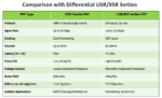
It becomes blatantly obvious when you look at the best industrial survey in verification conducted every two years by Harry Foster and Wilson Research. With only 68% of the ASIC/IC designs getting built the first time-around and the same number running late, the story of FPGA based designs is even worse – with only 17% hitting the first time-around mark. I’m not a pessimist, and every time I look at the trends of such reports it doesn’t make me feel that we are accelerating the deployment of the best verification methods known to mankind.

The Promise of Formal

Formal methods are a mathematical way of analysing requirements, providing clear specifications and makes use of computational logic under-the-hood to confirm or deny the presence of bugs in a model. This model can be a hardware design expressed as Verilog or VHDL, or any of the other languages such as Chisel, BlueSpec SV or even gate-level netlist. The only way of obtaining 100% guarantees that a given model doesn’t have functional defects or violates security or safety requirements is to verify it with the rigour of formal methods assisted with a great methodology.

A great methodology doesn’t exist in vacuum and is built as a collection of best practices on top of the technologies and describes ‘how’ these technologies can be used.

The how is therefore an important question to answer.

Challenge with formal methods: Lack of good training

One reason why formal methods adoption has been limited is because of the lack of know-how. While we may take a step back and understand the myriad reasons for this to be the case the foremost reason of why formal is not everyone’s cup of tea is because of lack of good comprehensive know-how. Formal methods have an exciting history with numerous landmark contributions from eminent computer scientists but for engineers it continues to be enigmatic. It is still perceived as an abstruse subject – the only exception is the use of apps by engineers thanks to the EDA companies who provided automated solutions to help solve bespoke problems. Formal market is now estimated to be 40% of the simulation. The automation provided easy-to-use tools that can provide an easy starting point on one end by the use of static lint analysis and on the other extreme end, solving problems like connectivity checking, register checking, X-checking, CDC and so on.

Between the two extremes, sits the rest of the interesting landscape of verification problems solvable through model checking also known as property checking as well as equivalence checking. Methodology is the key to success to everything and is no different for property checking. But a good methodology has to be on problem solving and should not tie you to a particular tool.

While I’m a huge fan of property checking and production-grade equivalence checking technologies, they do not solve all the verification problems. For example, if I’m interested in making sure that a compiler works correctly, or an inter-connect protocol model doesn’t have deadlocks, I may have to look beyond the run-of-the-mill property checking solutions. This is where theorem proving comes in.

Theorem provers do not suffer from capacity issues like dynamic simulation, or property checking tools and if you know to use them well, they can be used to verify theoretically infinite sized systems including operating systems and compilers as well as huge hardware designs.

There are several questions.

  1. Where do you go to learn about all these formal technologies?
  2. Why should you learn formal?
  3. What is formal?
  4. How does one find an accelerated path of learning formal with support without getting locked in a vendor tool?

Formal Verification 101

Welcome to Formal Verification 101 – the world’s first on-demand, self-paced, video course that provides a comprehensive introduction to all essential aspects of formal methods leading to a certification at the end.

This course comes with an online lounge accessible to the enrolled students where they can discuss any questions and engage with experts.

Let me first give you a personal perspective on why I decided to do this?

A Personal Perspective

Designed and delivered by yours truly, I took time to understand what has worked for me and what didn’t.  When I started learning formal over two decades ago, we did not have video courses in computational logic. While I took many courses in my master’s course, as an Electrical & Electronics engineer it was a steep learning curve. A large part of it was that we were not given a lot of practical perspectives. I was learning something in theory but didn’t know why and where it was useful.

I was lucky to work on my Doctorate with Tom Melham at University of Oxford and really lucky to have had a few hours with Mike Gordon from University of Cambridge who taught me how to use the HOL 4 theorem prover. If you’re not aware, both Tom Melham and Mike Gordon were one of the first few computer scientists using higher-order logic and formal for hardware verification. However, not everyone, can get the opportunities I got at Oxford and Cambridge.

I have been working in the industry on projects and have been training engineers in the industry in practical use of formal and have trained nearly 200 engineers including designers and verification folks in semiconductor industry. Working on cutting-edge designs, with shrinking time schedules gives me a strange sort of excitement and joy but teaching and sharing what worked and what didn’t equally give me a thrill. So, as it happens, I love sharing knowledge and enjoy teaching.

Two decades later

When I founded Axiomise, three years ago, there was still no video courses covering all the key formal technologies from an industrial perspective. In fact, there wasn’t a structured course covering all three formal technologies from an industrial perspective. There have been a few tutorials in theorem proving, or scanty material on property checking off and on, but no comprehensive introduction to all the key formal technologies in one place with a practical perspective delivered as a standalone course with online support.

Meanwhile, we built a range of instructor-led courses spanning from 1-day to 4-days that are designed to offer in-person tutorials in a structured manner covering theory, labs, and quizzes. The goal is to provide production-grade training to engineers in the industry. In its third year, this course is in demand and we continue to provide this training through face-to-face via Zoom. We issue certificates of completion. The main advantage of these courses is that I deliver them in-person. Students gain insights on real-world problems and get a chance to ask questions live during the training and get their hands dirty on hard problems where we learn together how to solve them.

Bridging the gap in industry

What we discovered was a gap in the industry and our own portfolio. Whereas our instructor-led courses are great for a newbie or a practising professional, these courses are not self-paced, and there is a commitment to multiple-days consecutively which can be a challenge for some people.  Formal Verification 101 course is designed to bridge this gap. You can take this comprehensive introductory course at your own pace, in your own time and learn the fundamentals of formal methods covering all the key formal technologies such as theorem proving, property checking and equivalence checking. We take an interactive approach to learning in this course by providing you with hands-on demos that you can redo yourself by downloading the source code, and gain experience of seeing formal methods in action. Once you’re comfortable with this course and pass the final exam and would like to explore more advanced concepts, you can take the multi-day instructor-led courses.

Expert Opinions

When I completed the course design, I invited several peers from industry and academia to take this course, review it and offer feedback.

I had to be conscious in choosing my first audience, so I wanted a spread the experience level, as much as geographic spread. We gave this course to Iain Singleton a formal verification engineer, Rajat Swarup – Manager at AWS, Supratik Chakraborty, Professor at IIT Bombay and Harry Foster, chair of the IEEE 1850 Property Specification Language Working Group.

They provided a candid and open feedback available to read on https://elearn.axiomise.com

Harry Foster humbled me with this comment.

“I’ve always said that achieving the ultimate goal of advanced formal signoff depends on about 20% tool and 80% skill. Yet, there has been a dearth of training material available that is essential for building expert-level formal skills. But not anymore! Dr Ashish Darbari has created the most comprehensive video course on the subject of applied formal methods that I have ever seen. This course should be required by any engineer with a desire to master the art, science, and skills of formal methods.”

With videos, text, downloadable source code, interactive demos, quizzes and a final exam leading to a certificate we have got everything covered for you. I’ve myself, sat down and recorded all the content, created the captions for all the videos so people with challenges can also enjoy the course.

It has been 20+ years of living in trenches, years of planning and several months of production that has gone in this work. I hope you will give this course a chance and join me in my love for formal.

Let us collectively design and build a safer and secure digital world. Sign up for the unique course in formal methods at https://elearn.axiomise.com.

Also read:

Life in a Formal Verification Lane

Accelerating Exhaustive and Complete Verification of RISC-V Processors

CEO Interview: Dr. Ashish Darbari of Axiomise


Podcast EP16: Hyperscale Computing & Changes in the Datacenter

Podcast EP16: Hyperscale Computing & Changes in the Datacenter
by Daniel Nenni on 04-16-2021 at 10:00 am

Dan is joined by Frank Schirrmeister, senior group director of solutions marketing at Cadence Design Systems, Frank has extensive experience in complex system design from his work at companies such as Cadence, Synopsys, Imperas and ChipVision. He has also advised Vayavya Labs and CriticalBlue.

Dan and Frank discuss the many challenges of building hyperscale datacenters and the innovations that are helping to make this massive compute infrastructure buildout a reality. Domain-specific compute architectures and the required design tool support are some of the items explored in this conversation.

The views, thoughts, and opinions expressed in these podcasts belong solely to the speaker, and not to the speaker’s employer, organization, committee or any other group or individual.


TSMC Ups CAPEX Again!

TSMC Ups CAPEX Again!
by Daniel Nenni on 04-16-2021 at 6:00 am

TSMC 1Q21 Revenue by Platform

We were all pleasantly surprised when TSMC increased 2021 Capex to a record $28 billion. To me this validated the talk inside the ecosystem that Intel would be coming to TSMC at 3nm. We were again surprised when TSMC announced a $100B investment over the next three years which belittled Intel’s announcement that they would spend $20B on two new fabs in Arizona.

It wasn’t clear what the TSMC investment included but we now know (via the Q1 2021 Investor Call) that it’s predominantly CAPEX starting with $30B in 2021 and the rest over 2022 and 2023. Personally, I think TSMC CAPEX will end up being more than $100B because TSMC tends to be conservative with their numbers, absolutely.

Let’s take a look at CC Wei’s opening statement on yesterday’s investor call:

CC Wei First, let me talk about the capacity shortage and demand outlook. Our customers are currently facing challenges from the industry-wide semiconductor capacity shortage, which is driven by both a structural increase in long-term demand as well as short-term imbalance in the supply chain. We are witnessing a structural increase in underlying semiconductor demand as a multi-year megatrend of 5G and HPC-related applications are expected to fuel strong demand for our advanced technologies in the next several years. COVID-19 has also fundamentally accelerate the digital transformation, making semiconductors more pervasive and essential in people’s life.

D.A.N. The short term imbalance is of course the drop in utilization last year due to the uncertainty brought by the pandemic and now the hockey stick shape rebound which includes some panic buying. The bottom line is that we have enough capacity today and more than enough capacity coming tomorrow so no worries here.

CC Wei: To address the structural increase in the long-term demand profile, we are working closely with our customers and investing to support their demand. We have acquired land and equipment and started the construction of new facilities. We are hiring thousands of employees and expanding our capacity at multiple sites. TSMC expects to invest about USD 100 billion through the next 3 years to increase capacity, to support the manufacturing and R&D of leading-edge and specialty technologies. Increased capacity is expected to improve supply certainty for our customers and help strengthen confidence in global supply chains that rely on semiconductors.

D.A.N. Based on what we have seen on the SemiWiki job board TSMC is indeed hiring thousands of employees and the TSMC job posts are getting 2x more views than average. And yes TSMC is already spending that $100B, $8.8B was consumed in Q1 2021.

CC Wei:  Our capital investment decisions are based on 4 disciplines: technology leadership, flexible and responsive manufacturing, retaining customers’ trust and earning the proper return. At the same time, we face manufacturing cost challenges due to increasing process complexity at leading node, new investment in mature nodes and rising material costs. Therefore, we will continue to work closely with customers to sell our value. Our value includes the value of our technology, the value of our service and the value of our capacity support to customers. We will look to firm up our wafer pricing to a reasonable level.

D.A.N. Translation: there will be pricing adjustments to compensate for the added capacity.

CC Wei:  Next, let me talk about the automotive supply update. The automotive market has been soft since 2018. Entering 2020, COVID-19 further impact the automotive market. The automotive supply chain was affected throughout the year, and our customers continued to reduce their demand throughout the third quarter of 2020. We only began to see sudden recovery in the fourth quarter of 2020.

However, the automotive supply chain is long and complex with its own inventory management practices. From chip production to car production, it takes at least 6 months with several tiers of suppliers in between. TSMC is doing its part to address the chip supply challenges for our customers.

D.A.N. Some car companies have shortages and some don’t, it all depends on inventory and who cut orders in 2020. Toyota I’m told has the best managed inventory and is still making cars. Other car companies not so much.

CC Wei: Finally, I will talk about the N5 and N3 status. TSMC’s N5 is the foundry industry’s most advanced solution with the best PPA. N5 is already in its second year of volume production with yield better than our original plan. N5 demand continue to be strong, driven by smartphone and HPC applications, and we expect N5 to contribute around 20% of our wafer revenue in 2021.

D.A.N. I was told by a gaming chip leaker that there is panic buying in crypto and gaming which may explain TSMC’s big HPC numbers. Also, the word inside the ecosystem is that Samsung is having problems so there is a burst of 5N and 3N design activity. In fact, 80% of the 2021 CAPEX is being spent on 5N and 3N (which are pretty much identical fabs using different process recipes).

CC Wei: N3 will be another full node stride from our N5 and will use FinFET transistor structure to deliver the best technology maturity, performance, and cost for our customers. Our N3 technology development is on track with good progress. We continue to see a much higher level of customer engagement for both HPC and smartphone applications at N3 as compared with N5 and N3 at a similar stage.

D.A.N. This is due to Samsung’s failure at 3nm. Scotten Jones did a nice blog on this earlier this year:

ISS 2021 – Scotten W. Jones – Logic Leadership in the PPAC era

CC Wei: Risk production is scheduled in 2021. The volume production is targeted in second half of 2022. Our 3-nanometer technology will be the most advanced foundry technology in both PPA and transistor technology. Thus, we are confident that both our 5-nanometer and 3-nanometer will be large and long-lasting nodes for TSMC.

D.A.N. Apple iProducts will be 3N next year which means HVM in 2H 2022. The IDM foundries (Intel and Samsung) do initial product introductions and spend a year or two ramping up to HVM so it is hard to compare new process introduction dates.

You can join a more detailed discussion here in the experts forum: TSMC Q1 2021 Earnings Conference Call


Enabling Next Generation Silicon In Package Products

Enabling Next Generation Silicon In Package Products
by Kalar Rajendiran on 04-15-2021 at 10:00 am

System on Package Motivation AlphaWave IP

In early April, Gabriele Saucier kicked off Design & Reuse’s IPSoC Silicon Valley 2021 Conference. IPSoC conference as the name suggests is dedicated to semiconductor intellectual property (IP) and IP-based electronic systems. There were a number of excellent presentations at the conference. The presentations had been categorized into eight different subject matter tracks. The tracks were Advanced Packaging Solution and Chiplet, Analog and Memory Blocks, Design and Verification, Interface IP, Security Solutions, Automotive IP and SoC, Video IP and High-Performance Computing.

Semiconductor Packaging as a technology has garnered lot of investment and attention for many years now. We have had various innovations over the years including flip-chip, silicon interposer, 2.5D, 3D, chip scale packaging and wafer level packaging. Many of these advances were driven by the need to overcome device performance limitations, signal-integrity issues, form-factor constraints and/or simply market acceptance price points. So, the “advanced packaging solution and chiplet” track piqued my interest and I listened in on some of the presentations.

One of the presentations I listened to was titled “Enabling Next Generation Silicon In Package Products” and was presented by Tony Pialis, the CEO of Alphawave IP, Inc.

There is a long history of successful system-in-a-package (SiP) products launched by different companies. One reason for going the SiP route is faster time to market (TTM). By mixing and matching IP that pre-exist in different process technologies, the time, effort and cost of having to port the different IP blocks to the same process technology is avoided. System-in-a-package interchangeably referred to as silicon-in-package is not a new concept.

So, why was Tony’s presentation under the Advanced Packaging track? This blog addresses that question through salient points gathered from Tony’s talk. For complete details, please register and listen to Tony’s entire talk.

Next generation products are expected to see broader and faster adoption of SiP. As sub-10nm process node becomes main stream, two strong reasons for SiP adoption come into play (see Figure 1). The first reason: System-on-a-chip (SoC) development cost crossing the $500M mark. That is a 20X increase compared to the cost of developing an SoC in 65nm process node. The second reason revolves around die yield and number of good dies per wafer. The yield rate is better for smaller dies. Here in lies the opportunity to benefit economically, if all technical challenges can be overcome.

Figure 1: Opportunity from an Economic Perspective


Technical Challenges:

Achieving the economic benefits requires disintegrating an SoC die into smaller dies. In this context, these smaller dies are being termed chiplets. Simplistic definition of a chiplet: a die that holds a functional circuit block. But this approach of partitioning into chiplets introduces many challenges. A number of nanometer pitch wires that were on-chip now turn into package-level interconnects, thereby introducing signal integrity issues. longer latencies, increased power and test complexities.

Technology Solutions:

The good news is that manufacturing capabilities in the form of silicon interposer, through-silicon-vias and chip scale packaging technologies already exist to enable chiplets integration. The focus is now on chiplet interfaces to eliminate the signal integrity, latency and power issues. At a basic level, partitioning of an SoC leads to chiplets that are primarily logic bound, memory bound or I/O bound. The chiplet type determines what type of interface makes sense and what interface standards are available/supported.

Parallel interface implementations such as the Bunch of Wires (BoW) interface which is an Open Domain-Specific Architecture (ODSA) sub-committee supported standard, and the Advanced Interface Bus (AIB) interface which is an Intel/DARPA supported standard are well suited for use with logic bound chiplets.

The High Bandwidth Memory (HBM) interface standard, which is well established and in wide use is more suited for memory bound chiplets.

Serial interface implementations such as the XSR (extra short reach) and the USR (ultra short reach) interfaces are well suited for use with I/O bound chiplets.

In his presentation, Tony discusses lot of details in terms of supported speeds, latencies, power, bandwidth, etc., for each of these interface types. He delves deep into Alphawave IP’s DieCORE 112Gbps XSR interface IP and discusses ways of managing bit error rate (BER) performance.

If interested in benefiting from a chiplets implementation approach, I recommend you register and listen to Tony’s entire talk and then discuss with Alphawave IP on ways to leverage their different IP offerings for developing your products.

Also Read:

CEO Interview: Tony Pialis of Alphawave IP

Alphawave IP and the Evolution of the ASIC Business

Alphawave IP is Enabling 224Gbps Serial Links with DSP


Low Energy SoCs with Near Threshold Voltage

Low Energy SoCs with Near Threshold Voltage
by Tom Simon on 04-15-2021 at 6:00 am

Low Energy Efficiency

There is an important difference between low power and low energy in SOC design. Low power focuses on instantaneous power consumption. This is frequently done to deal with cooling and heat dissipation issues. Of course, it serves as a prerequisite for low energy design, which seeks to reduce overall power consumption over time. Low energy is desired when energy is limited, such as in a battery, photovoltaic or other energy harvester. Low energy systems either have to get a certain amount of processing done with the available energy supply or they may have to preserve system operating life.

One of the most obvious techniques for reducing energy consumption is to reduce the operating voltage of the system. This can reduce dynamic energy consumption proportionally to the square of the voltage. Operating at or near threshold voltages offers big savings in energy consumption. So why not deploy it widely?

Low Energy Efficiency

In a video recording of a DAC presentation by Minima Processor’s CTO Lauri Koskinen titled “Near Threshold Voltage: A Much Needed Reality or Risky Dream?” the pros and cons of near threshold operation are discussed. Without giving too much away, it is clear that near threshold voltage operation is an important arrow in the quiver of things that can be done to reduce system energy consumption. However, several specialized techniques need to be employed to maintain system performance and yield in chips intending to take advantage of this approach.

Lauri points out in his presentation that there is a minimum energy point for devices that is very close to the threshold voltage. If you overlay the maximum operating frequency (Fmax) on this, it is evident that for many applications the work per unit of energy can be optimized. Yet, this can be at a point where variation causes extreme shifts in device performance. Lauri points to evidence showing that subthreshold operation can cause 20X greater performance deltas due to random variation than operation at higher voltages.

Lauri asserts that near threshold operation offers great benefits without the difficulties of subthreshold, but still needs specialized techniques to make it commercially effective. Lauri points out that with specialized libraries and the use of advanced voltage scaling (AVS) that good results have been achieved. He presents several near threshold chips that have been designed over the years using standard design flows. They range from 180nm down to 14nm, all having very impressive low energy consumption.

He wraps up by reviewing the key success factors that will provide a path forward to low energy SOCs that can be used in products that require long battery life or operating times with alternative power sources. AVS and dynamic voltage and frequency scaling (DVFS) are first on his list. The latest EDA tools have capabilities that will support this type of design. He points out that there will have to be additional types of test methodologies to handle these designs. Beyond the methods above, allowing higher levels of granularity and intelligence in creating voltage islands and power domains is a powerful technique to ensure overall system performance while being miserly with energy consumption.

It is becoming more common for wireless devices to offer 10 year battery life. For instance, we see this in household lighting applications for remote wireless switches. Industrial applications and other uses where battery replacement or provisioning will create extra costs will be candidates for the most aggressive possible energy savings. Also, applications like earbuds call for maximizing useful life. We can expect to see more advanced and intelligent approaches to solving these challenges. If you want to view the entire DAC presentation given by Minima’s Lauri Koskinen it can be viewed here on their website.


Global Variation and Its Impact on Time-to-Market for Designs

Global Variation and Its Impact on Time-to-Market for Designs
by umangdoshi on 04-14-2021 at 2:00 pm

Impact of Global Variation on Delay

We have come a long way from the days of limited and manageable characterization databases with fewer views and smaller library sizes. The technologies we are headed towards pushing characterization to its limits with special modeling for variation, aging and reliability all on a single process, voltage and temperature (PVT). Additionally there is a requirement to generate basic nominal timing/noise/power views as well as more complex variation views.

With the advancement in technology and the push towards smaller nodes from 7nm down to 3nm, the designs are expected to work under different modes, with possibly different clock frequencies along with a range of global variations. Thus, the designs have to achieve signoff closure for timing and power across an enormous number of PVT corners. Characterizing these huge number of PVT corners, library teams across the industry face further challenges like high simulation turnaround time, database disk-space, license server overloads and hardware costs. All of these result in overall impacting adversely the time-to-market delivery of designs in a cost-effective manner.

Characterizing multiple PVT corners can be done using multiple methodologies. One such is brute-force method, where using many compute resources runs all possible PVT corners required in parallel and thus reduces the overall turn-around time (TAT). Another method is to characterize timing data for nominal while scaling the Liberty Variation Format (LVF) data, which is about 60-70% of the overall runtime for library characterization, thus achieving 2-4X faster TAT. Both these methods have their pros and cons -while the compute cost to generate all libraries in parallel is significantly higher, the libraries are very accurate, whereas for scaled LVF data the compute cost is lower, but with a possible sacrifice in accuracy.

Not only does Synopsys offer a feature for scaling LVF data to generate SmartLVF (as illustrated in Figure 2) libraries for multiple PVT corners, we have developed an advanced ML-based scaling feature called SmartScaling which fits right into this requirement space to provide the much-required relief for designers. SmartScaling for multi-PVT characterization enables designers to create interpolated Liberty models at zero cost while maintaining signoff accuracy. This significantly reduces overall runtime and alleviates concerns of database management thus providing the most accurate, cost-efficient solution.

With an easy-to-use UI to accept user-defined anchor libraries over a range of conditions, SmartScaling can quickly create libraries at other corners as chosen by the user. While this is the most basic usage, it also offers further advantages to adaptively select anchor corners to get best scaling accuracy, accept user-controlled custom indices, do some cross-PVT trend checks and then some more!

Designer’s needs may vary – from simply creating structurally consistent placeholder Libs for end- to-end flow flush to producing accurate intermediate PVT’s for signoff – and the solution is SmartScaling.

Summary

Multi-PVT characterization has become necessary to generate libraries that include model variations, aging and reliability data at the most advanced nodes. This imposes an increased demand for computing resources needed for characterization which increases time-to-market and overall cost for the design. Synopsys’s SmartScaling for multi-PVT characterization improves the runtime significantly to provide over 3X increase in efficiency and reduce overall cost.

With latest innovation in Synopsys’s library characterization, achieve faster and more accurate variation models with the goal of generating PrimeTime® signoff quality libraries. Learn more about the close collaboration and integration between various signoff products at www.synopsys.com/signoff

Also Read:

VC Formal SIG Virtually Conferences in Europe

Key Requirements for Effective SoC Verification Management

Techniques and Tools for Accelerating Low Power Design Simulations