RVN! 26 Banner revised (800 x 100 px) (600 x 100 px)

How to Spend $100 Billion Dollars in Three Years

How to Spend $100 Billion Dollars in Three Years
by Scotten Jones on 04-25-2021 at 6:00 am

Slide1 1

TSMC recently announced plans to spend $100 billion dollars over three years on capital. For 2021 they announced $30B in total capital with 80% on advanced nodes (7nm and smaller), 10% on packaging and masks and 10% on “specialty”.

If we take a guess at the capital for each year, we can project something like $30B for 2021 (announced), $33.5B for 2022 and $36.5B for 2023. $30B + $33.5B + $36.5B = $100B. The exact breakout by year for 2022 and 2023 may be different than this but overall, the numbers work. If we further assume that the 80% spending on advanced node ratio will be maintained over the three years, we get: $24B for 2021, $26.8B for 2022 and $29.2B for 2023 ($80B total).

What kind of advanced capabilities can you buy for $80B over 3 years?

Figure 1 illustrates our view of TSMC’s advanced node plans.

Figure 1. TSMC Advanced Node Plans.

To begin 2021, TSMC had record 7nm revenue in Q1 and we believe they needed to add 25K wafer per month (wpm) of capacity to do that, whether that spending was in 2021 or late 2020 is subject to debate. 5nm was in production beginning in the second half of 2020 and we believe a farther ramp up of 60k wpm will take place in 2021 reaching 120k wpm by year end. Also, in late 2021 will be 3nm risk starts requiring the completion of one cleanroom phase and an estimated 15k wpm of 3nm capacity.

2022 will see the ramp up of 3nm with an additional 60K wpm of capacity.

2023 Will see the build out of 5nm capacity at the Arizona fab, and an additional 45k wpm of 3nm capacity. Finally, we expect 2nm risk starts in 2023 requiring a cleanroom build out and 15k wpm. Where 5nm and 3nm are being produced in 3 cleanroom phases each, TSMC has announced that 2nm will be built in four cleanroom phases and we have planned on two phase in 2023.

Figure 2 illustrates our view of TSMC’s capital spending by node for 7nm, 5nm, 3nm and 2nm.

Figure 2. TSMC Capital Spending on Advanced Nodes.

In 2021 we have $4.6B for 7nm capacity, $15.2B for additional 5nm capacity and $6.4B for the initial 3nm cleanroom and risk starts capability. The total $26.3B is more than the calculated $24B so some of the 7nm capacity may be in 2020 or some of the 3nm spending may be in 2022.

In 2022 we have $23.2B for additional 3nm capacity, this is less than the $26.8B expected for 2022. Because 2023 is expected to have spending in Arizona, more 3nm capacity and the initial 2nm build out it is possible 2022 may see less capital spending than we initially assumed and 2023 more capital spending.

For 2023 we have the first 5nm phase built out in Arizona for $5.7B, additional 3nm capacity for $15.4B and the initial build out of 2nm for $9.3B. The total for 2023 is $33.5B, more than the estimated $29.2B.

If we add up our forecast over three years, we get $79.8B versus the $80B estimate assuming 80% of the announced $100B is spent on advanced nodes. We should also keep in mind that the $100B is a three-year estimate subject to changing market conditions.

In this scenario, in 2023 TSMC will have 140k wpm of 5nm production capacity, 120k wpm of 3nm production capacity and 15k wpm of 2nm risk start capacity.

Also Read:

SPIE 2021 – Applied Materials – DRAM Scaling

Kioxia and Western Digital and the current Kioxia IPO/Sale rumors

Intel Node Names


Podcast EP17: EDA, Semiconductors and the Future

Podcast EP17: EDA, Semiconductors and the Future
by Daniel Nenni on 04-23-2021 at 10:00 am

Dan and Mike are joined by semiconductor and EDA executive Jack Harding. Jack has a diverse career as a technology executive beginning at IBM with notable stops along the way, including taking Cooper and Chyan Technology public, taking the helm from Joe Costello as CEO of Cadence and most recently as the founding CEO of eSilicon, which was acquired by Inphi.

Jack advises industry, academia and government on matters of technology and innovation. He is a frequent international speaker on the topics of innovation, entrepreneurship and semiconductor trends and policies. We discuss Jack’s path to EDA and semiconductors, with some key observations about the business,  We conclude with an assessment of some megatrends and a look to the future.

The views, thoughts, and opinions expressed in these podcasts belong solely to the speaker, and not to the speaker’s employer, organization, committee or any other group or individual.


Automakers to Blame for Semiconductor Shortage

Automakers to Blame for Semiconductor Shortage
by Bill Jewell on 04-23-2021 at 8:00 am

Top Automotive Semiconductor Suppliers

Automakers worldwide have scaled back production due to a shortage of semiconductors. Companies which have announced temporary halts on production include Volkswagen, Toyota, General Motors, Ford, Nissan, Honda, Suzuki, Mitsubishi, Daimler (Mercedes) and Stellantis (merger of Fiat-Chrysler and Peugot).

IHS Markit estimates 1Q 2021 light vehicle production was reduced by 1.3 million units due to the shortage. They stated the semiconductor shortage may not be resolved until 4Q 2021. Microcontrollers (MCUs) are in particularly shot supply. IHS Markit estimates 70% of MCUs are manufactured by Taiwan Semiconductor Manufacturing Co. (TSMC), the worlds largest semiconductor foundry. In its 1Q 2021 quarterly conference call, TSMC stated they have worked to reallocate wafer capacity to support the automotive industry. TSMC expects the automotive semiconductor shortage for its customers to be largely resolved by 3Q 2021.

The largest automotive semiconductor suppliers are listed below. The automotive revenues are based on the companies’ financial reports. The revenues for STMicroelectronics are for its Automotive & Discrete Group, which includes some non-automotive revenues. However, ST also has automotive products such as MCUs and sensors in its other product groups. Infineon’s automotive revenue increased 1.1% for its fiscal year ended September 2020. The other companies all saw declines in 2020 versus 2019 ranging from 4% to 9%.

Several of these companies rely on TSMC and other foundries for much of their wafer production. Each company also has its own wafer fabs. Some of these fabs have recently encountered production problems. EETimes reports Infineon and NXP had to temporarily shut down their wafer fabs in Austin, Texas due to electricity outages during severe winter storms in February. NXP said the shutdown could reduce 2Q 2021 revenue by about $100 million. Infineon expects a hit to its revenues in the current quarter but expects to make up the revenues in the next quarter.

Renesas had a fire at is Naka, Japan wafer fab in March. The Japan Times reports Renesas expects the fab to return to full production in late May. The fire could cost Renesas up to 24 billion yen (US$220 million) in lost revenue.

Texas Instruments stated it will be able to meet demand for its products including automotive. TI produces most of its semiconductors at its own wafer fabs. ON Semiconductor said it has the capacity to support its automotive semiconductors and expects to catch up with demand by 2Q 2021 or 3Q 2021. STMicroelectronics also manufactures most of its wafers at its own fabs and expects to be able to meet the demand for automotive semiconductors.

The shortage of automotive semiconductors is primarily the fault of the auto makers. When the global COVID-19 pandemic began in early 2020, automakers cut production. Some of the production cuts were to protect workers from exposure to COVID-19. Most of the production cuts were due to the uncertain demand for autos in the wake of major economic disruption caused by the pandemic.

The top ten automotive (light vehicle) manufacturers are listed below. The number of vehicles is either production (when available) or sales from company reports. These ten companies account for about 70% of all light vehicles made. All had declines in vehicles in 2020 versus 2019, ranging from 10% to 27%. Collectively, the ten companies had a 17% decline in vehicles in 2020.

Vehicle production declines began in 1Q 2020. SAIC Motor of China had a 56% decline in 1Q 2020 production versus a year earlier, primarily due to factory shutdowns to try to contain COVID-19 spread in China. Other automakers had year-to-year declines in 1Q 2020 ranging from 9% to 27%. In 2Q 2020, SAIC Motor production returned almost to normal production levels. All other makers experienced major production declines in 2Q 2020 versus a year earlier, ranging from 24% to 63%. By 4Q 2020 production had returned to normal levels, with year-to-year change ranging from a 5% decline for Volkswagen to a 11% gain for Honda.

The automotive production decline is illustrated below compared to two other major end markets for semiconductors, PCs and smartphones. Shipments are indexed to 1Q 2019 equaling 100. The change in units shipped each quarter is based on the quarter-to-quarter change against the base index. Vehicle units dropped to 60% of 1Q 2019 levels in 2Q 2020, before recovering in 4Q 2020. PCs and smartphone units shipped dropped to about 90% of 1Q 2019 levels in 1Q 2020. PC shipments grew strongly in 2Q 2020 to 4Q 2020, reaching over 150% of 1Q 2019 shipments. Smartphone shipments were flat in 2Q 2020 versus 1Q 2020 but recovered to over 120% of 1Q 2019 shipments in 4Q 2020.

There are numerous other applications for semiconductors, but these represent the general trend. One cannot blame semiconductor companies for switching capacity to growing applications while automakers cut production (and presumably semiconductor orders) by 40% over two quarters. It will take time to resolve the shortages. TSMC stated it takes at least six months from semiconductor production to auto production and involves several links in the supply chain. Capacity can be shifted in the short term, but increasing overall capacity often requires construction of new wafer fabs, which takes about two years. Automakers gave up their place in line, so they will have to wait their turn for semiconductors.

Semiconductor Intelligence is a consulting firm providing market analysis, market insights and company analysis for anyone involved in the semiconductor industry – manufacturers, designers, foundries, suppliers, users or investors. Please contact me if you would like further information.

Bill Jewell
Semiconductor Intelligence, LLC
billjewell@sc-iq.com

Also Read:

Electronics Back Strongly in 2021

Semiconductors up 6.5% in 2020, >10% in 2021?

Semiconductor Boom in 2021


CEO Interview: Dr. Rick Shen of eMemory

CEO Interview: Dr. Rick Shen of eMemory
by Daniel Nenni on 04-23-2021 at 6:00 am

eMemory Business Model

Dr. Shen has been President of eMemory Technology since 2009, succeeding Dr. Charles Hsu. Prior to the appointment, Dr. Shen held various management positions within the company, overseeing Technology Development, founding the Customer Service team, supervising Technology & IP services, and the company’s technology development migration from 0.7um to 90nm. Dr. Shen received his doctoral degree in Electrical Engineering from National Tsing-Hua University (NTHU). He holds over 80 worldwide patents, has published 25 technical papers, and co-authored the book “Logic Non-Volatile Memory”.

Dr. Shen was one of the key inventors of eMemory’s proprietary NVM technology portfolio. He was integral in establishing the company as the world’s most reliable One Time Programmable (OTP) memory partner and continues to lead the eNVM IP industry under his guidance. He was a named recipient of the ‘National Invention and Creation’ Gold Medal, for his work developing eMemory’s NeoBit Technology and was presented with NTHU’s prestigious ‘Outstanding Alumni Award’ in 2018.

How did eMemory get started?
We established eMemory back in the year 2000. Dr. Charles Hsu, our Chairman, was a professor at National Tsing Hua University where his research group was focused on the design and physics behind Non Volatile Memory (NVM), particularly novel cell structure, operation schemes, and the aging mechanism analysis of its reliability. Almost all of the founding team back then, including myself, had studied under Charles.

We were perhaps the only startup at the time with an Academic background researching NVM. It was a pivotal time in the industry and early on, we received many inquiries from companies seeking out new solutions. There was a high demand for a novel low-voltage or low-power memory solution that could reduce production costs and enable new applications. The traditional NVM technology on the market was very complex, often requiring many additional masks during fabrication, and often, far more features than the products required. Our Logic NVM solution changed all that. We were matching the market demand by providing a fully CMOS process compatible solution, with less processing whilst removing the need for ‘extra’ masks. It was, frankly, a big breakthrough in the sector.

What added value do bring to your customers? 
I think there are three consistent challenges that our customers face, enhancing performance, improving product yields, and reducing cycle time. That push to improve quality and reliability without compromising development time has been the driver of the semiconductor industry over the last 20 years. The lifecycle of each new product gets shorter as the end-user moves onto the next generation faster than ever before. A component can take 1-2 years to develop now, which is just too long for our customers to respond to market demand. So, that means it is essential that our IPs are widely qualified and available across new technology platforms. We want to have our IPs ready before the customer knows that they need them.

I think if you look at our investment in R+D, you can see a clear correlation to the value we are adding to customers. This business is driven by innovation and we always want to look for what’s next. For example, I think our Chip Fingerprint Technology, based from our OTP technology, will become essential to our customers in the future. It’s going to play a big role in ending reverse engineering, protecting data, and enabling zero-trust security om securing the IoT for our customers by utilizing Physical Unclonable Function (PUF) based technology.

What makes eMemory unique?
As a physical IP company, developing innovations like our OTP device and integrating into hard IPs, definitely sets us apart. There are only a handful of physical IP companies and as such, we think differently about our role as an IP provider and get involved in the whole process as much as possible, from design to fabrication.

We have seen our IPs integrated on over 400 process platforms and Cross the Chasm into the mainstream IP market. That is a lot of effort working together with our foundry partners, and for our competitors, a lot of catching up to do. We don’t take commercial successes for granted however, we know how changeable this sector can be, so for us, innovation is something you need to sustain and never look away from. It is often missed just how specific and highly process-sensitive the memory field is. That is why we also place such a premium on technical support and expertise. We want to allow our customers to concentrate on product design and then rely on us to have high-quality NVM IPs and support them with a full spectrum of technical engineering services.

We have received for 11 consecutive years now the ‘Best IP Partner Award’ from TSMC. That is something we are very proud of because it demonstrates not just eMemory’s reliability but more importantly, that our IPs have remained innovative for over a decade now. We work with 24 foundries and are part of over 500 tape-outs every year. The vast majority of our business is returning partners who trust us with, not only the technology advancement, but also highly sensitive information related to their specifications, planning, and schedules. Some of these relationships stretch back decades, which for us is the biggest compliment.

What is your business model?
Our business model focuses on collaborating with both the foundries and the design houses. On the foundry side, we are a technology provider collecting royalties, with the Design houses, we license our IP block design and for both, we offer technical support. It can be easy to overlook that we are all part of the manufacturing process and not just theoretically designing circuits in front of a screen. It is only when the foundry is fully considered in the design and process development stages that reliable and practical solutions can be found.

We want to have a memory block that best meets our customer needs and that naturally includes a seamless transition from design into production. For eMemory, that means creating a triangular partnership between the design house, the foundry, and ourselves. This creates a much closer collaboration among all three parties and allows eMemory to take an active role in supporting the product development all the way to completion. We have found this to be the most reliable model, and one that benefits everyone. When it works, we are all rewarded and if any issues do arise, we are all invested in finding a quick solution. We have seen consistently stable production yields with a high level of reliability for many years now as a result.

What is next for the company?
We will of course continue to innovate our logic embedded NVM technologies and employ them over many applications. Moving into more advanced process nodes is also a priority, particularly with our OTP and Multiple Time Programmable (MTP) memory IP, where we want to widen the availability of our portfolio and cater to emerging memory technologies like ReRAM and MRAM. I think our current positioning inside the industry leaves us primed to take advantage of these shifts in the market.

Our recent IP NeoPUF, which is a Hardware Root of Trust, we believe will also be a big part of our future as we expand into PUF-based hardware solutions and services. It may seem on the surface that Hardware Security is an entirely different business proposition to our customers but the underlying physics have the same fundamentals. Our NeoPUF IP derives from our OTP technology, which is already extensively qualified. The OTP platform, now with PUF IP, can allow our customers to adopt a zero-trust hardware security solution quite easily and protect them from reverse engineering and adversarial attacks.

Hardware security is set to become an essential part of the Internet of Things (IoT) and 5G in the future as the necessary level of connectivity between devices only heightens the risk to security. Spending on hardware security has always been a calculation of risk management, and we think within the semiconductor market, that calculation is currently undervalued. We hope to play a big part in securing the future of our connected world over the next decade.

Also Read:

CEO Interview: Kush Gulati of Omni Design Technologies

Executive Interview: Casper van Oosten of Intermolecular, Inc.

CEO Interview: R.K. Patil of Vayavya Labs


Using eFPGA to Dynamically Adapt to Changing Workloads

Using eFPGA to Dynamically Adapt to Changing Workloads
by Kalar Rajendiran on 04-22-2021 at 10:00 am

Dynamic Reconfig Not New Why Now FlexLogix

In early April, Gabriele Saucier kicked off Design & Reuse’s IPSoC Silicon Valley 2021 Conference. IPSoC conference as the name suggests is dedicated to semiconductor intellectual property (IP) and IP-based electronic systems. There were a number of excellent presentations at the conference. The presentations had been categorized into eight different subject matter tracks. The tracks were Advanced Packaging Solution and Chiplet, Analog and Memory Blocks, Design and Verification, Interface IP, Security Solutions, Automotive IP and SoC, Video IP and High-Performance Computing.

One of the presentations under the high-performance computing (HPC) track was by Andy Jaros, VP IP Sales and Marketing at Flex Logix. The talk was titled “Using eFPGA to Dynamically Adapt to Changing Workloads.

As we know, current FPGA company landscape is very different compared to even a few years ago. Altera was acquired by Intel a few years ago. Xilinx is going through the process of merging with Advanced Micro Devices (AMD). Many of the FPGA startups of yester years are no longer around. At the same time, there are some new companies whose differentiated technologies are experiencing market adoption success. But embedded FPGA in itself is not a new product offering. And dynamically adapting to workloads is not a new concept.

So, I listened to Andy’s talk with the goal of understanding why the market would want the solution more, this time around. This blog includes a summary of what I gathered from Andy’s talk. For complete details, please register and listen to Andy’s presentation.

Flex Logix has an embedded FPGA (eFPGA) IP business unit and an Edge Inferencing Solutions co-processor chips business unit. It has more than a dozen working-silicon chips using eFPGA, an almost equal number of chips in design and an additional two dozen chips in the pipeline. It recently closed a $55M Series D funding round. And it generates strong profits from its eFPGA IP business.

Right at the outset Andy acknowledges that dynamic reconfigurability is not new. The concept has been pursued since the late 1990s. But it didn’t take off then for a number of reasons.  In a nutshell, the concept was ahead of its time. Refer to Figure 1.

Figure 1:

Fast forward to today, market has changed a lot. Chip development costs a lot more and takes much longer than it did 10 to 20 years ago. Accelerators are drivers of next generation performance, not process nodes. Edge computing applications are driving the need for handling dynamic workloads. These applications have to work on instant data and make decisions in real time at the user end level. As a result, more throughput/$ is more critical than raw throughput. This is where dynamically adapting to workloads becomes attractive and rapid reconfigurability gets the job done.

Andy uses their InferX X1 chip implementing a neural network model to demonstrate dynamic reconfigurability concept in action. Refer to Figure 2.

Figure 2:

It is good idea to understand what is driving dynamic workload variations. This will highlight the value of reconfigurability and the importance of very fast reconfiguration times.

Many applications these days leverage artificial intelligence (AI) techniques in their implementations. AI techniques use neural network models to capture complex non-linear relationships and involve multiple layers of parallel computations between the input and output stages. Each layer may necessitate more or less computations to perform relative to the amount of memory that layer requires. This causes dynamically varying workloads that need to be executed in real time.

InferX X1 is able to reconfigure the resources into optimized hardware accelerators for each layer of the model as that layer is executed, reconfiguring in 4 microsecs between each layer. That’s incredible.  Andy talks about three use cases for applicability of eFPGA dynamic reconfigurability that can be supported today and says faster InferX type of implementation can be supported with EFLX.

Andy explains the software development flow for implementing reconfigurability using eFPGA cores and EFLX compiler. In essence, Flex Logix’s eFPGA platform makes it easy to implement reconfigurable hardware accelerators and integrate into a customer’s chips. Key workloads can be expected to execute 10-100x faster compared to general purpose processors.

He wraps up his presentation with availability status of Flex Logix’s silicon proven EFLX cores in different process nodes ranging from 40nm down to 7nm in foundries including TSMC and Global Foundries.

If you find this interesting, I recommend you listen to Andy’s entire talk and then discuss with Flex Logix for ways to leverage their product offerings for a great solution to your customer base.


Embedded Analytics Becoming Essential

Embedded Analytics Becoming Essential
by Tom Simon on 04-22-2021 at 6:00 am

Embedded Analytics

SoC integration offers huge benefits through reduced chip count in finished systems, higher performance, improved reliability, etc. A single die can contain billions of transistors, with multiple processors and countless subsystems all working together. The result of this has been rapid growth of semiconductor content in many old and new products, including automotive, networking, telecommunications, medical, mobile, entertainment, etc. While higher levels of integration are largely beneficial, there are new challenges with system level integration, debug and verification. Embedded Analytics will play an important role in implementing and verifying these large and complex systems.

Many SoCs have large numbers of blocks and subsystems connected through on-chip bus or network interfaces. They use on-chip memory and registers and incorporate complex software running application code. In previous generations system level observation and debug were challenging but made possible through what were previously external connections or in-circuit emulators (ICE). Modern SoCs require a completely new approach to understand dynamic system operation with sufficient visibility and control to make sense of what is occurring during operation.

Siemens EDA writes about this in a white paper called “Embedded Analytics – A platform approach”. They cite the causes of increased design complexity leading to increased difficulty in design, optimization, verification and lifecycle management.

First on their list is multi-source IP, where one SoC will contain IP from numerous sources, both internal and external. These IP elements can include heterogenous processors, interfaces, and a host of other kinds of blocks. Next comes the software for each of these processors. The software could be algorithmic or for managing chip operations or security. Each of these software packages in turn will probably be built on a software stack.

Complexity in these SoCs can come from hardware and software interactions. The Siemens white paper correctly points out that often the kinds of problems caused by these interactions are non-deterministic and efforts to observe them can make them disappear or change behavior. The cost of system level validation can cost tens of millions of dollars. Functional validation needs to start early in the design process through to system installation. System level interactions need to be examined using simulation, emulation, prototyping and in finished systems. Even after product shipment, software updates can cause system level issues that will need to be investigated.

By now it is clear that system level visibility into hardware and software is necessary. Without enough detail it may be difficult to pinpoint problems. On the other hand, too much data can also be an issue. The white paper points out that a truly effective observation and data gathering system for SoCs needs to have sophisticated control over what data is collected and when.

Embedded Analytics

Siemens EDA has developed the Tessent Embedded Analytics platform to allow system designers to wrap their hands around the problems relating to system level real time observation and analysis. There are several pieces to this platform, allowing it to be integrated with the target SoC and then be used to collect and interpret data on system operation.

Tessent Embedded Analytics has an IP subsystem that is integrated into the target SoC. This IP is easily parameterized to make integration efficient and easy. There is also a hierarchical message passing fabric used to transfer the collected data efficiently with minimal added silicon overhead. The message passing fabric can handle local or cross-chip data transfers and is separate from the mission mode interconnect.

To help filter the data collected there are programmable filters, counters and matchers that enable smart and configurable data filtering and event triggering in real time at the frequency of the SoC. There are secure data links for collecting data and interacting with the outside world. Tessent Embedded Analytics contains a software interface layer that communicates between the application layers and the analytics IP.

The Tessent Embedded Analytics platform includes the tools to create applications that interact with its IP components to enable sophisticated monitoring of the SoC. There is a software development kit (Embedded SDK) that lets user developed applications configure, control and process the analytics data. The Configuration API, Data API and Verification API are available for use in either the Tessent Embedded Anaytics IDE or 3rd party IDE environments through plugins.

The Siemens white paper describes in more detail how the entire process works and how it can support prototyping through FPGAs or emulators, as well as in-system silicon. Without an embedded analytics platform, system designers face an almost intractable problem when it comes to verifying and optimizing present day SoCs. Siemens seems to appreciate that while an embedded analytics platform must be comprehensive, it must not require excess silicon resource or interfere with system operation. The full white paper is worth reading to gain a better understanding of how Siemens EDA has assembled a powerful solution for these difficult challenges. The white paper is available on the Siemens EDA website.

Also Read:

Siemens EDA Updates, Completes Its Hardware-Assisted Verification Portfolio

Formal for Post-Silicon Bug Hunting? Makes perfect sense

Library Characterization: A Siemens Cloud Solution using AWS


Adaptive Power/Performance Management for FD-SOI

Adaptive Power/Performance Management for FD-SOI
by Tom Dillinger on 04-21-2021 at 10:00 am

Dolphin FD SOI FBB

A vexing chip design issue is how to achieve (or improve) performance and power dissipation targets, allowing for a wide range of manufacturing process variation (P) and dynamic operation voltage and temperature fluctuations (VT).  One design method is to analyze the operation across a set of PVT corners, and ensure sufficient design margin across this multi-dimensional space.  Another approach is to dynamically alter the applied voltages (globally, or in a local domain), based on sensing the changing behavior of a reference circuit.

The introduction of fully-depleted silicon-on-insulator (FD-SOI) device technology has led to a resurgence in the opportunities for incorporating circuitry to adaptively modify the device bias conditions, to compensate for PVT tolerances.  This interest is further advanced by the goals of many applications to operate over a wider temperature range, and especially, to operate at a reduced VDD supply voltage to minimize power dissipation.

At the recent International Solid State Circuits Conference (ISSCC 2021), as part of a collaboration with GLOBALFOUNDRIES and CEA-Leti, Dolphin Design presented an update on their IP offering to provide adaptive body bias (ABB) to FD-SOI devices to compensate for PVT variation and optimize power/performance, with minimal overhead. [1]  This article provides some of the highlights of their presentation.

Background

For decades, designers have implemented methods to modify circuit performance based on real-time sensor feedback.

One of the first techniques addressed the issue of PVT variation on the output current of off-chip driver circuits – a critical design parameter is to maintain an impedance match to the package and printed circuit board traces to minimize signal reflections.  A performance-sense ring oscillator (odd inverter chain) delay was used as a real-time PVT measurement.  The frequency of the PSRO was compared to a reference, and additional parallel devices were added/disabled to the off-chip driver pullup and pulldown device stacks – see the figure below. [2]

Another method that was commonly used to adjust the operational behavior was to dynamically alter the substrate bias applied to the design.  Recall that the threshold voltage of the FET is a function of the source-to-substrate voltage difference across the semiconductor p-n junction – by modulating the substrate bias, the Vt would be adjusted and the variation in circuit performance improved.  (As the magnitude of the junction reverse bias increases, Vt increases as well;  reducing the reverse bias reduces the Vt magnitude and improves performance.  A small bulk forward bias is also possible to further improve performance – e.g., ~100-200mV – without excessive junction diode current.)

In the very early nMOS processes, the p-type substrate was common to all devices (enhancement-mode and depletion-mode nFETs).  A charge pump circuit on the die generated a negative Vsub, periodically pulling capacitive-coupled current out of the substrate.  By sensing a reference device Vt real-time, the duration and/or magnitude of this charge pump current could be modified. [3]  For a 5V nMOS process, with a nominal Vsub = -3V, there was plenty of range available to modify the back bias.

The transition to CMOS processes introduced the need to consider both the p-substrate and n-well as potential body bias nodes.  Designers developed a strategy for inserting p-sub and n-well taps throughout the die to connect to bias supplies, separate from the VDD and GND rails connected to the circuitry.

With the ongoing Dennard CMOS scaling associated with Moore’s Law, body bias techniques were less viable.  The additional reverse-bias electric field across the junction is a breakdown issue at scaled dimensions.  As a result, Vsub typically became the same rail connection as GND, and Vnwell was the same rail as VDD.  If distinct substrate bias control to the devices was required, CMOS processes were extended to include a triple-well option – see the figure below.

An additional p-well inside a deep n-well inside the p-substrate allowed unique reverse-bias voltages to be applied to the n-well (pMOS) and local p-well (nMOS) devices.

Rather than using body bias, designers increasingly looked to adjust the VDD power supply for PVT compensation, a technique commonly denoted as dynamic voltage, frequency scaling (DVFS).  Parenthetically, the use of DVFS methods was expanded beyond adaptive compensation for a target frequency to also provide boost modes of higher frequency operation at higher supplies, as well as a variety of power management states at reduced supply values.  (And, the market for PMICs exploded, as well.)

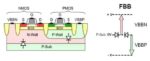
The introduction of SOI device technology – and FD-SOI, in particular – changed the landscape for adaptive body bias techniques.  A FD-SOI cross-section is shown in the figure below.

Note the use of the triple-well fabrication technique, allowing a unique back bias to be independently applied to nMOS and pMOS devices.  Also, note the devices shown above are different than the conventional CMOS process technology.  The nMOS above is situated above an n-well, while the pMOS is situated above a p-well – this topology would be reversed in a typical CMOS process.  This unique FD-SOI process option is used to implement low Vt devices.

The presence of the thin isolating buried dielectric layer (BOX) below the device channel re-introduces the option of applying a p-well and n-well bias.  This technique involves etching the well contacts through the (thin) silicon channel and dielectric layers of the FD-SOI device.

The p-n junction breakdown electric field issues of scaled CMOS are eliminated – the allowable electric field across the BOX dielectric is greater.

The FD-SOI device topology shown above offers the opportunity to apply an effective forward bias to the body, reducing the threshold voltage magnitude and boosting performance. (In a conventional CMOS process, the nMOS device would be subjected to a reverse bias relative to the channel, applied to the p-substrate.)

The BOX dielectric isolates the channel region – there is no source/drain-to-substrate diode junction.  Note that bias restrictions remain for the p-n junctions of the device wells below the BOX.

Although the forward body bias technique increases the device leakage current, the supply voltage required to meet the target frequency can be reduced, with an overall power savings – more on that shortly.

Thus, there is renewed emphasis on the integration of ABB circuitry for FD-SOI designs, to compensate for PVT variations and/or optimize the operational frequency and power dissipation.

Dolphin ABB IP

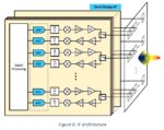
A block diagram of the ABB IP is shown below.

A primary input to the IP is the target operational frequency for the controlled domain, Ftarget.  (For the Arm Cortex M4F core testcase design, the Ftarget was in the range ~10MHz – 1.5GHz.)

A coarse timing lock to this target is provided by a frequency-lock loop (FLL) circuit, comprised of a (digital) frequency comparator that generates adjust pulses to modulate the currents into n-well and p-well.  Specifically, the lock is based on two separate divider ratios, R and N, one for Ftarget and one for an internally generated clock, Finternal.  Lock is achieved when (Ftarget/R) = (Finternal/N).

The internally-generated clock reference for the frequency-lock loop in the ABB controller also includes PVT sense circuitry, to reduce the variation in the ring-oscillator frequency.

When the coarse monitor-based FLL is locked, the dynamic fine-grain adaptive bias is enabled.  The detailed adjust to the n-well and p-well current drivers uses feedback from timing monitors distributed throughout the design block to be controlled by the ABB IP.

As voltage(s) and temperature(s) within the block fluctuate, the monitor(s) signal the ABB controller to increment/decrement the divider ratio “N” to adjust the well current drivers, maintaining the lock to the target frequency, as illustrated in the figure below.

The implementation of the ABB IP is all-digital for the FLL control and feedback, and the distributed timing monitors in the block.  The exception is the charge pump circuitry that provides the p-well and n-well currents – in the Dolphin ABB IP, a VDDA=1.8V supply is used, the same supply as provided to the I/O cells.  This enables a range of back bias voltage values from the charge pump.

Testsite and Measurement Results

The Dolphin team incorporated the ABB IP with an Arm Cortex M4F core, in a 22nm FD-SOI testsite fabricated at GLOBALFOUNDRIES – see the micrograph below, with the related specs.

For this testsite, Dolphin chose to implement the Arm core using LVT-based cells and forward-body bias, with the device cross-section shown above.  The focus of this experiment was to achieve the target frequency at a low core supply voltage, thereby reducing overall power dissipation.  The available forward body bias values were:

  • LVT nMOS – Vnw:  0V to 1.5V (FBB)
  • LVT pMOS – Vpw:  0V to -1.5V  (FBB)

Measurement data examples are shown below, illustrating how the Vnw and Vpw bias voltage varies with sweeps in temperature and supply voltage, to maintain lock to the target frequency.

Note that the independent current sources for the p-well and n-well imply that these bias voltages may be asymmetric.

Of critical importance is the ability to use ABB to reduce the (nominal) core supply voltage, while maintaining the target frequency specification.  For this design testsite, the use of LVT cells and ABB with forward bias enabled a reduction of ~100mV in the supply, while still meeting the target frequency – e.g., from 0.55V to 0.45V.  This results in a ~20% overall power savings, as illustrated below (shown across three temperature corners, including both the power dissipation of the Arm core and the additional ABB IP).

Summary

FD-SOI technology has reinvigorated the interest in using adaptive body bias techniques for maintaining the operational target frequency over PVT variations.  Both reverse-body bias (RBB) and forward-body bias (FBB) techniques can be applied, to RVT and LVT device configurations.  At the recent ISSCC, Dolphin Design demonstrated how their ABB IP integrated with a core block can utilize FBB to achieve and dynamically maintain a target frequency.  This technique relaxes the corner-based design margin constraints that typically define the supply voltage – a low supply can be selected, with the corresponding power savings.

Here is a link with additional information on adaptive body bias techniques in FD-SOI – link.

-chipguy

References

[1]  Moursy, Y., et al., “A 0.021mm**2 PVT-Aware Digital-Flow-Compatible Adaptive Back-Biasing Regulator with Scalable Drivers Achieving 450% Frequency Boosting and 30% Power Reduction in 22nm FDSOI Technology”, ISSCC 2021, paper 35.2.

[2]  Dillinger, T., VLSI Design Methodology Development, Prentice-Hall, 2019.

[3]  US Patent # US-4553047, “Regulator for Substrate Voltage Generator”.


Arm Announces v9 Generation – Custom, DSP, Security, More

Arm Announces v9 Generation – Custom, DSP, Security, More
by Bernard Murphy on 04-21-2021 at 6:00 am

Balance of Standardization min

This wasn’t as much of a big bang announcement as others I have seen. More a polishing of earlier-announced reveals, positioning updates, together with some new concepts. First, you probably remember the Cortex-X announcement from about a year ago, allowing users to customize their own instructions into the standard instruction set. A response to similar flexibility in RISC-V. I get the impression this started as a tactical response to specific customer needs. Understandable, but you could see how that could get of control as interest spreads more widely. Richard Grisenthwaite, Sr VP, Chief Architect and Fellow at Arm talked about rationalizing standardization versus customization in a spectrum of support. Details not revealed yet but makes sense.

Who’s interested?

Richard nodded to the Fugaku supercomputer in his talk, that they possibly took advantage of this v9 flexibility. And he nodded to AWS Graviton2, as another potential beneficiary. But he added that really the rush to differentiate dominates every place we compute, from the cloud to the edge. Hence the balancing act in v9. Preserving all the benefits of standardization and compatibility with a massive ecosystem. While still allowing integrators to add their own secret sauce.

There’s more

That’s not all there is to v9. They have launched a rolling program with enhancements to machine learning, DSP and security in CPU, GPU and NPU platforms. Take machine learning first. Arm continues to stress that the range of ML-applications can’t be met with a one-size-fits-all solution. So they continue to extend support in A, M and R processors, working closely with colleagues at NVIDIA. (Jem Davies followed with more detail on this topic.)

DSPs?

This one took me a little by surprise. Looking backward, Arm didn’t make much noise about DSPs. Perhaps because they didn’t see a big enough opportunity? But the range of DSP-related applications has been exploding. In automotive for infotainment audio, communication, sensing, driver alertness, road noise suppression, V2X. More in consumer audio (wireless earbuds for example). No doubt again a spectrum of needs where Arm sees an opportunity for enhanced standard processors rather than dedicated DSPs? Richard didn’t elaborate.

He did however mention that the scalable vector extensions (SVE) they developed with Fujitsu for Fugaku. Expecting this capability to be extended to a much wider range of applications. He mentioned they have already created SVE2 to work well with 5G systems. I assume baseband applications you might normally expect high-end processors or DSPs to fill today. That can only be good; room for more kinds of embedded solution.

Security

Arm continues to emphasize security and thank goodness for that because I see no other central force to drag us towards building secure distributed systems. Impressively a following panel on this topic included a panelist from Munich RE Group. Investors care about liabilities. The easy-going days of “we can figure this out on our own” are drawing to a close.

Arm see security stakes being raised by distribution of compute between edge devices and compute nodes through wireless and backhaul networks. Application developers and service providers will want to run tasks where it makes most sense, without having to worry about which compute nodes have what security.

Here Richard talked about a confidential compute architecture to preserve data security. Arm plans to reveal more details on this architecture later in the year. One concept they will introduce is dynamically created realms, zones in which ordinary programs can run safely, separate from the secure and non-secure zones we already understand. Service customer apps and data need to be ensured high levels of security, yet the current view of secure versus insecure zones on a device doesn’t really address that need. (Where would such a task run? In the secure zone? Heck no. In the insecure zone? Ditto.) Realms provide a separate computation world outside the secure and non-secure zones, designed to depend on a small level of trust in the rest of the system. Even if a hack compromises components of the system, an app and its data running inside a realm can still be secure.

More security extensions on the way

Arm has also been working with Google on memory tagging extensions to protect against the memory safety issues we will never eliminate in our software. They’ve been working with Cambridge University on their Capability Hardware Enhanced Risk Instruction-Set Architecture (CHERI) to further bound vulnerabilities, all the way down to the ISA level. And they’re working with the UK government on a program called Morello, designed to bound the scope of any breach that does get a foothold.

Lots of interesting work: rationalization of the extensions program, more ML-everywhere and an interesting start into DSP markets. You can read the press release HERE.


Addressing SoC Test Implementation Time and Costs

Addressing SoC Test Implementation Time and Costs
by Daniel Payne on 04-20-2021 at 10:00 am

testmax flow

In business we all have heard the maxim, “Time is Money.” I learned this lesson early on in my semiconductor career when doing DRAM design, discovering that the packaging costs and time on the tester were actually higher than the fabrication costs. System companies like IBM were early adopters of Design For Test (DFT) by adopting scan design with special test Flip-Flops and then using Automatic Test Pattern Generation (ATPG) software to create test implementations that had high fault coverage, with a minimum amount of time on the tester.

It took awhile for logic designers at IDMs to adopt DFT techniques, because they were hesitant to give up silicon area in order to improve fault coverage numbers, instead favoring the smallest die size to maximize profits.

Challenges

Today there are many challenges to test implementation time and costs:

  • Higher Design Complexity
    • >100,000,000 cell instances
    • 100’s of cores
  • Subtle Defects
    • >50% of failures not found with standard tests
  • In-system testing required
  • Fewer test pins
    • Designs/core with <7 test pins

Consider a modern GPU design that has 50 Billion transistors, with 100 million cell instances, just how do you create enough test patterns to meet fault coverage goals while spending the minimum time on a tester?

A Solution

Adding scan Flip-Flops is a great start and a proven DFT methodology, but what if you want to meet these newer challenges?

It’s all about controllability and observability in the test world, and by adding something called a Test Point, you make controlling and observing a low coverage point in your logic much, much easier. Consider the following cloud of logic, followed by a D FF:

If the D input to the FF is difficult to control, or set, then we never observe a change in the output at point B. By adding a Test Point, we can now control the D input, thus improving the fault coverage:

Ideally, a test engineer wants to use Test Points that are compatible with existing scan compression, having minimal impact on Power/Performance/Area (PPA), and is easy to use.

Synopsys TestMAX Advisor

I spoke with Robert Ruiz, Director of Product Marketing, Test Automation Products and Pawini Mahajan, Sr. Product Marketing Manager, Digital Design Group over a Zoom call to learn how the Synopsys TestMAX Advisor tool fits into an overall suite of test tools. Robert and I first met back in the 1990s when he worked at Sunrise Test Systems, and I was at Viewlogic, so he has a deep history in the test world. Pawini and I both worked at Intel, still the number one semiconductor company in the world by revenue.

Here’s the tool sub-flow for TestMAX Advisor:

The TestMAX Advisor tool will analyze and rank all of the FFs used in a design, then determine which nets need added controllability or observability, so a test engineer can then determine just how many Test Points should be inserted and see how much the fault coverage improvement and shorter test patterns are going to be. The engineer can even set the percentage coverage goals and allow TestMAX Advisor to add Test Points automatically to meet the goals.

Side note to users of other ATPG tools, yes, you can use TestMAX Advisor with your favorite ATPG tool.

You get to see the incremental fault coverage improvement by adding Test Points in a table format:

Test Implementation

Adding extra Test Points is going to add new congestion to the routing, so the developers figured out how to make the placement of Test Points be physically-aware, so that congestion is minimized and timing impacts are reduced. Just look at the congestion map comparison below:

Seven examples of fault coverage improvements (up to 30%)  and pattern count reductions (up to 40%) were provided:

Summary

DFT using scan and ATPG tools is recommended to achieve fault coverage goals, and when shortest test times are important then you can consider adding new Test Points to improve controllability and observability. EDA developers at Synopsys have coded all of the features to make Test Point insertion an easy task that is producing some promising results to address the test implementation time and costs. TestMAX Advisor looks to be another worthy tool in your toolbox.

Related Blogs

5G Calls for New Transceiver Architectures

5G Calls for New Transceiver Architectures
by Tom Simon on 04-20-2021 at 6:00 am

5G Architecture

5G phones are now the top tier devices from many manufactures, and 5G deployment is accelerating in many regions. While 4G/LTE has served us well, 5G is necessary to support next-generation telecommunication needs. It will be used heavily by consumers and industry because it supports many new use cases. There is an excellent white paper by Omni Design Technologies that discusses the new applications for 5G, the technological changes that are necessary, and the hardware architectures needed to support it.

The white paper, titled “5G Technology and Transceiver Architecture” lists the three main use cases as enhanced mobile broadband (eMBB), ultra-reliable and low-latency communications (URLLC), and massive machine-type communications (mMTC). Each has specific technical requirements aligned with the scenarios that each will be used for. Each will vary in terms of peak data rate, spectral efficiency, latency, connection density, reliability, and many more.

Consumers will see 4k and 8k streaming, AR/VR improvements and much lower latency and higher speed access to the cloud. To fully realize higher bandwidth 5G will open up new communications bands from 24GHz to 100GHz. URLLC will be used for applications that require real-time performance, like automotive or some industrial applications. It calls for 1ms latency and 99.999% reliability. mMTC will be used for billions of connected devices such as wearables, IoT and sensors that use lower bandwidth and require low power.

I already alluded to one of the key technologies, millimeter-wave (mmWave), that will be essential to 5G. The white paper says that 5G deployment is going to move first and most rapidly in the sub-6GHz bands with the help of infrastructure reuse. The bands above 24GHz will offer much greater bandwidth but come with additional technical complexity. One of the key issues is that propagation losses will be much higher due to obstacles and signal absorption in the atmosphere.

MIMO will be used to improve signal performance through spatial diversity, spatial multiplexing and beamforming. Spatial diversity takes advantage of multipath to gain information using multiple antennas. The different antennas see different signals that can be used to mathematically determine the transmitted signal. Spatial multiplexing creates multiple spatially separated signals between the transmitter and receiver to boost data rates.

As a consequence of technology changes the hardware architecture for 5G is also changing. Beamforming is one of the biggest drivers for changes we see in the hardware implementation. The white paper points out that current commercial solutions include 64TX and 64RX for base station deployments. This is a large increase from the 2×2 or 4×4 arrays used in 4G.

It is no longer feasible to perform all the beamforming operations in pure analog or pure digital. If a pure digital approach is used, then each array element must have its own RF chain. This causes increased power consumption and adds components. Going with a pure analog approach requires only one RF chain but gives up a lot of the reconfigurability and spatial resolution.

5G Architecture

Omni Design suggests that a hybrid approach can meet all system objectives and is easier to implement. Much of the processing can be done on the digital side. Fewer RF chains are needed, with the analog side handling phase shifting individually for each antenna. Omni Design offers data converter IP solutions for 5G applications. Their IP is suited for below 6GHz or above 24GHz, using an IF architecture. Their solutions are offered in multiple processes from 28nm to advanced FinFET nodes. Omni Design has patented technologies that enable data converters to operate at higher sampling rates and precision while significantly reducing power consumption.

The white paper goes into detail on the performance characteristics of their IP for 5G. It also talks about the verification requirements and how their IP offering includes the necessary deliverables to ensure rigorous verification. With much of the 5G deployment still ahead of us, there will be an increasing need for data converter semiconductors. The Omni Design white paper, which is available here, is a good source of information useful for teams working to develop products for 5G telecommunication systems.