RVN! 26 Banner revised (800 x 100 px) (600 x 100 px)

CEO Interview: Aki Fujimura of D2S

CEO Interview: Aki Fujimura of D2S
by Daniel Nenni on 03-18-2022 at 6:00 am

ESD Alliance D2S Blog Post Image 1 1

Curvilinear Design Primer for Design, Packaging Communities

This interview was done by Bob Smith, Executive Director, ESD Alliance, a SEMI Technology Community.

Previously, Fujimura served as CTO at Cadence Design Systems and returned to Cadence for the second time through the acquisition of Simplex Solutions where he was President/COO and inside board member. He was also an inside board member and VP at Pure Software. Simplex and Pure both went public during his tenure. Fujimura was a founding member of Tangent Systems, subsequently acquired by Cadence Design Systems. He was a board member of HLDS, RTime, Bristol, S7, and Coverity, Inc., all of which were successfully acquired. Fujimura received Bachelor of Science and Master of Science degrees in Electrical Engineering from MIT.

Semiconductor packaging and photomask segments of our industry have undergone some major technology changes in the past few years after relatively minor changes for many years. In the case of photomasks, new technologies such as multi-beam mask writers and extreme ultraviolet (EUV) lithography are major breakthroughs in the news as they ramp into high-volume manufacturing. A new trend related to these technologies is the use of curvilinear features on photomasks.

Curvilinear photomasks are here today, particularly interesting to the ESD Alliance as the door opens for “curvy” design. Aki Fujimura, CEO of D2S and a member of the the ESD Alliance Governing Council, speaks to me about curvilinear photomasks and what it means for design and packaging.

BS: What are the advantages of curvilinear photomasks?

AF: First let me explain what we mean by curvilinear photomasks. Shapes consisting of axis-parallel edges are sometimes referred to as Manhattan geometries. Shapes that do not need to be Manhattan geometries are considered curvilinear in the context of our discussion.

Curvilinear mask features have been shown not only to print more accurately, mostly because 90-degree corners can’t be accurately reproduced, but also to print more reliably, with less variation. This is good for both mask and wafer quality.

BS: What breakthroughs enabled curvilinear photomasks?

AF: Multi-beam mask writing and GPU-acceleration of pixel-based computing including curvilinear inverse lithography technology (ILT) are enabling curvilinear masks. With multi-beam mask writers available in all leading-edge mask shops now, the mask write times are no longer affected by the number of shapes on the mask or their complexity. This is principally because multi-beam mask writers write with pixels, similarly to how TVs, monitors, and digital projection machines work.

The economics of mask writing is dominated by the mask writing time. The fact that multi-beam mask writers, given a resist and writing method, writes any shapes of any shape count in constant time is economically and logistically very attractive to the mask shop. Once a mask shop has a multi-beam mask writer, curvilinear masks take no more time to write than any other.

BS: What is ILT and how does it contribute?

AK: ILT is a mathematically rigorous inverse version of optical proximity correction (OPC) known to produce the best wafer results for both optical (193i) and EUV lithography. Many studies have demonstrated that curvilinear ILT mask shapes produce the best “process windows,” a measure of resilience to manufacturing variation.

Until multi-beam mask writers became available in the leading-edge mask shops, it hadn’t been practically possible to use curvilinear mask shapes as the desired mask shapes provided to the mask writers. However, runtimes associated with this computational technique limited its practical application to critical “hotspots” on chips.

Applying GPU acceleration to the ILT problem paved the way in the past few years for some breakthroughs in runtime roadblocks to ILT. In 2019, an entirely new approach systematically designed for multi-beam mask writers and GPU acceleration by D2S made full-chip ILT a practical reality in production for the first time.

BS: Will curvilinear masks be used for 193i lithography, EUV or both?

AF: In annual surveys conducted by the eBeam Initiative (See Figure 1), industry experts anticipate that curvilinear ILT shapes are already in use or will be for hotspots in some leading-edge layers before 2023 for both 193i and EUV masks. They clearly indicate that the primary reason to purchase multi-beam mask writers is for EUV masks. They also indicate that writing curvilinear masks is also a strong reason to purchase multi-beam mask writers.

Given that EUV masks are being written with multi-beam mask writers already, there is no penalty in the mask write time to write curvilinear shapes. Whether for 193i or for EUV, curvilinear mask shapes produce better wafer quality. With sufficient supply of multi-beam writers, leading-edge masks are likely to be written with them in the future.

Figure 1 caption: 2020 eBeam Initiative Survey result in answer to the question: “How extensively will curvilinear shapes be used for leading-edge (EUV, 193i) masks intended for high-volume manufacturing (HVM) by 2023?” (a) 94% believe curvilinear shapes will be used for 193i for HVM by 2023, (b) 85% expect that EUV also needs curvilinear shapes for HVM.

Source: eBeam Initiative

BS: Where is the industry in terms of adoption of curvilinear photomasks?

AF:  With multi-beam mask writing being widely available for the leading-edge nodes, manufacturing curvilinear ILT shapes is now possible.

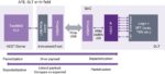
And the rest of the mask making infrastructure shown in Figure 2? A limited number of curvilinear shapes can already be handled by leading-edge mask shops today, according to leading authorities. For wide-spread use, there are likely more streamlined solutions needed for metrology, inspection, dispositioning and repair.

Figure 2 caption: A typical photomask manufacturing flow follows a specific pattern.

Source: D2S

BS: How do curvilinear photomasks unlock new opportunities for design?

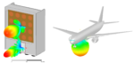
AF: As we anticipate this exciting transition to curvilinear mask making or “curvy” design, an upstream effect of this change is being studied by some. Figure 3(a) below shows an image from an Imec paper in 2019 that highlighted potential improvements in compacting cell designs, decreasing load, and decreasing interconnect delay through the use of curvy design. Figure 3(b) from a Micron presentation illustrates the use of manual manipulation to jog multi-bit busses using non-Manhattan, curvilinear shapes of varying angles. Manual manipulation is resource intensive, a clear indication of the benefits being significant enough to be worth the trouble, at least for a memory maker. The entire chip design infrastructure is based on the Manhattan assumption.

In my previous life in EDA, I had something to do with that, so I know this very well and it is not going to change any time soon. At the same time, though, is there any doubt that a curvilinear chip, if magically made possible, would be smaller, faster, and use less power?

Figure 3 caption: (a) An Imec paper showing “curvy” designs are feasible with the reliable manufacturing of curvy masks, (b) an example wafer image from Micron with non-Manhattan design.

Source: D2S

Also Read

CEO Interview: Frankwell Lin, Chairman and CEO of Andes Technology

CEO Interview: Tamas Olaszi of Jade Design Automation

CEO Interview: John Mortensen of Comcores


5G and Aircraft Safety: Simulation is Key to Ensuring Passenger Safety – Part 4

5G and Aircraft Safety: Simulation is Key to Ensuring Passenger Safety – Part 4
by Shawn Carpenter on 03-17-2022 at 10:00 am

RA 5G Chan3 KingAirField Scenario thumbnail 1

In our previous blog installments, we examined the ingredient for modeling the potential for interference between a 5G C-band base station and an aviation radar altimeter. Using candidate emissions models for the transmitter, wideband susceptibility models for a candidate radar altimeter receiver and antenna and propagation models for the wireless channel, we arrived at an analysis for a worst-case static arrangement of the systems. In addition, we explored a potential interference mitigation technique to eliminate the in-channel interference experienced by the radar altimeter which involved the design of a low-pass filter for the 5G base station.

Next, we add the component of real-world motion.

Dynamic Interference Assessment: Interference Simulation for an Airport Approach

To better understand the way interference might occur during a landing, takeoff, or go-around, we need to simulate the scenario as it unfolds during the flight process. This requires simulating the interference situation during the flight sequence in an accurate virtual environment involving a particular runway of interest.

Variations in the flight path and aircraft dynamics should be considered to determine worst-case scenarios for interference situations. These could include aircraft roll during landing due to wind gusts and turbulence, which could rotate the aircraft radar altimeter antenna to stare into a nearby 5G C-band base station on the ground. They could also include the impact of low-height base stations and propagation interactions with buildings and structures near the ground and around the airport.

Exploring these cases through experimental flight will be extremely costly and require control of the airspace and the electromagnetic spectrum around the airport during testing. Repeating these experiments for each of the variables listed above is simply untenable. But with modeling and simulation, we can explore these scenarios virtually and automatically, yielding the top scenarios that may warrant a final flight test for measurement-based validation. In fact without simulation, it is unrealistic to expect that all scenarios could be checked out experimentally within six months.

We have assembled such a simulation for a landing scenario near King County International Airport in Seattle, Washington. The figure below displays a landing scenario set up in the Ansys AGI Systems Tool Kit (STK) software. A notional long-range, wide-body aircraft is shown with the antenna pattern for an installed radar altimeter system. The landing trajectory is shown by the blue line on a south-by-southeast heading, which includes a taxi distance on the runway after landing. A 5G C-band base station antenna system is indicated directly under the flight path, with a mounting height of 9.5m, at or below roofline height of nearby buildings. AGI STK includes local terrain in scenarios, and even Mt. Rainier is visible in the distance.

Figure 11 – Landing approach scenario in AGI STK for an aircraft at King County International Airport in Seattle, WA. Simulated approach includes time-indexed flight dynamics, including aircraft pitch and roll effects on radar altimeter antenna pointing.

The aircraft will pass quite close to the 5G C-band base station in this scenario as shown in the figure below, but we have the freedom to place and move our base station antennas anywhere we wish, enabling rapid re-evaluation of the scenario.

Figure 12 – STK simulation shows landing geometry as aircraft passes close to the 5G C-band base station in the scenario. Projection of the radar altimeter gain contours can be seen on the ground beneath the aircraft.

The radios used in this simulation are identical to those defined in the static interference analysis, with the notable exception that the out of band saturation power level for our radar altimeter receiver is -30 dBm. It should be noted that this does not reflect the actual radar altimeter system installed on a particular aircraft, but is simply a notional system design based on the range of radar altimeter systems presented in the RTCA report to the FAA dated Oct. 2020.

Antenna-to-Antenna Coupling Captured with Physics

An important addition to this simulation is the use of high-fidelity physics simulation in computing the antenna to antenna coupling from moment to moment during the scenario. Recall that each antenna pattern has its basis in an electromagnetic simulation by Ansys HFSS and HFSS SBR+ to capture installed radar altimeter antenna effects as well as to capture an accurate radiation pattern for the 5G C-band phased array antenna.

The antennas are set into a model of the larger scattering environment that includes tower, buildings and large scattering structures around the airport, and the antenna-to-antenna coupling is sampled by HFSS SBR+. With this solution approach, potential masking and multi-path reflections by nearby buildings and structures are included in the physical path coupling from C-band 5G base station to radar altimeter antenna. S-parameter coupling data can be computed for a single frequency or a high number of frequencies sampled across any band of interest.

Interference Scenarios for the Current and Future 5G C-band Channel Implementations

The video below shows the complete landing scenario as simulated. In the inset graph, the electromagnetic interference (EMI) margin is illustrated. EMI margin represents the interfering transmitter spectral power present across the band of interest in the radar altimeter receiver front end, minus the receiver’s ability to reject that power. When the EMI margin (black curve) rises above the red line, the potential for interference exists and the receiver is either saturated (by a strong out of band signal) or de-sensitized (by a strong in-band signal). In addition, the EMI margin legend on the plot is color-coded to signify interference at any time. Green indicates an interference-free operation in the band, blue and yellow indicate EMI margins that have crossed indicator thresholds near interference conditions, and red indicates an interference event is occurring. The following simulation is conducted with a 5G C-band system operating in the current band of 3.7-3.8 GHz:

We can see strong interference occurs as the aircraft passes over the 5G C-band tower. The radar altimeter registers interference within its operational channel (centered at 4.2 GHz), and the receiver is also saturated from the strong 5G signals that are outside of the radar altimeter’s intended band of operation.

We can easily change the 5G C-band transmitter definition in our simulation to consider interference potential when the telecom operator uses the 80 MHz band from 3.9 to 3.98 GHz. Because it is closer to the radar altimeter band, we might expect that the potential for interference to the radar altimeter to be enhanced, and a quick re-simulation reveals this to be the case:

How to Fix to 5G C-Band Airport Issues

With modeling and simulation within scenario modeling, we can explore any radar altimeter, on any aircraft, at any airport runway, against any C-band 5G service towers that exist within a given radius of any airport. Given models of sufficient fidelity, this can all be done on a computer by individuals at any location without requiring flight time or impacting airport operations. Using simulation, we could:

  • Explore or modify existing or planned radar altimeter systems
  • Explore or modify 5G C-band base station performance parameters
  • Examine cases where multiple 5G C-band base stations might exist
  • Examine edge cases with respect to aircraft flight landing/takeoff dynamics (roll/pitch) which could result in antennas looking into one another’s high-gain zones
  • Examine and explore reasonable limits on power, beams teering, effective isotropic radiated power (EIRP), and modifying 5G service tower keep-out zones around airports
  • Provide guidance on flight planning for helicopters, private aircraft, delivery drones and more

Interference between the adjacent C-Band 5G spectrum services and radar altimeter systems is both predictable and solvable. Given sufficient fidelity in the underlying models, simulation represents a cost- and time-effective way to unobtrusively test and validate potential interference scenarios for any aircraft at any runway location. Scenarios can go beyond considering just 5G towers near the airport — with tools like AGI STK and Ansys Electronics Desktop we can look at any combination of wireless systems that might exhibit interference potential. This could become a key enabler for functions like low-altitude flight planning for helicopters, urban air mobility, drone delivery systems, and more.

Also read:

5G and Aircraft Safety: Simulation is Key to Ensuring Passenger Safety

5G and Aircraft Safety: Simulation is Key to Ensuring Passenger Safety – Part 2

5G and Aircraft Safety: Simulation is Key to Ensuring Passenger Safety – Part 3


Balancing Test Requirements with SOC Security

Balancing Test Requirements with SOC Security
by Tom Simon on 03-17-2022 at 6:00 am

Secure Test for SOCs

Typically, there is an existential rift between the on-chip access requirements for test and the need for security in SoCs. Using traditional deterministic scan techniques has meant opening up full read and write access to the flops in a design through the scan chains. Having this kind of access easily defeats the best designed functional mode security. With so many new applications requiring security, it is essential to eliminate any security holes created because of test.

Furthermore, test has moved from being something done only during manufacture, to an ongoing requirement to monitor chip operation. New approaches are needed to fulfill expanding needs and at the same time close down any avenues that might compromise chip security. Siemens EDA has written a white paper that outlines how a wide range of techniques can be utilized separately or together to provide security in depth. Interestingly many of these techniques are already extremely desirable from a strictly test perspective.

The white paper titled “High-quality test and embedded analytic solutions for secure applications” written by Lee Harrison talks about the need for secure test and illustrates a series of techniques that are very useful. At the core of each of these techniques is the notion that there should be no direct connection between the external test pins and the internal scan chain. Without this separation the chip can be probed and even controlled with ease. Fortunately, many of the innovations for test to meet speed, capacity and flexibility requirements have the added benefit of abstracting access to the scan chains themselves.

The Siemens white paper describes a progression of techniques, starting with logic built-in self test (LBIST) that secure the scan mechanisms on SoCs. The benefits of LBIST are multifold, offering in system test, speeding up test time and comes with added benefit that it seals off the scan chain from direct external access. However, LBIST without a BIST bypass mode can limit the ability to diagnose  failures. So additional methods such as adding security features to the test access point (TAP) controllers may be needed.

Test compression is another effective way to limit direct access to the scan chains. Conveniently it also is useful for other directly related test improvements, such as reducing tester data transfer volume. Tessent TestKompress is already widely used for testing chips for smart cards and defense related designs where it adds a layer of security. Test compression screens both the input and output of the scan chains.

Further isolation and encapsulation of the scan chains is achieved through the Tessent Streaming Scan Network (SSN). Here all of the scan data is packetized and transmitted through a dedicated on-chip test network. Of course, as above, there are many practical benefits and reasons to deploy an SSN. It offers full isolation of the scan chains which can only be accessed electrically by the SSN nodes embedded within the chip.

Secure Test for SOCs

The Siemens white paper provides insights into several other methods that can improve security while meeting the needs of testability. Foremost among these is upgrading the interface to the TAP controller so that it is in a safety island. This safety island can use a state-of-the-art security manager to limit access based on security needs. It also makes it possible to offer different levels of secure access depending on whether the chip is still on-premise during manufacture or deployed in the field as part of a system.

The white paper makes good reading and offers useful information for anyone looking to tighten up security through this potentially risky portion of their design. The white paper can be downloaded here through the Siemens website.

Also read:

Siemens EDA on the Best Verification Strategy

Scalable Verification Solutions at Siemens EDA

Power Analysis in Advanced SoCs. A Siemens EDA Perspective


5G and Aircraft Safety: Simulation is Key to Ensuring Passenger Safety – Part 3

5G and Aircraft Safety: Simulation is Key to Ensuring Passenger Safety – Part 3
by Shawn Carpenter on 03-16-2022 at 10:00 am

Fig 7 HFSS Antenna Patterns

In our previous blog installment, we introduced the components of RF interference modeling, and established models for wideband peak emissions of a 5G C-band transmitter and the wideband receiver susceptibility for a radar altimeter receiver. Here, we consider the third component: the wireless channel, which considers the physics of the antennas and how they couple energy in the environment. After we establish parameters for the wireless channel, we will be in a position to combine all three to get an accurate estimate of the maximum interference potential at any frequency.

Antenna-to-Antenna Coupling

Modeling interference accurately depends upon having accurate models for coupling the power coming out of the transmitter to the receiver — across the entire band. This is important for both in-channel coupling as well as out-of-band emissions coupling. Measurement of antenna coupling is challenging because of the spacing between the antennas and the fact that the radar altimeter antenna is in continual motion.

The wireless channel of Figure 4 (in the previous blog entry) consists of the 5G transmit antenna and its characteristics for focusing power in a given direction, the radar altimeter antenna and its directional gain sensitivity, and the propagation (and loss) of the signal as it travels between the two antennas. For accurate antenna performance, Ansys HFSS can be used to accurately predict the antenna behavior through electromagnetic simulation, to capture beamforming performance and the way the antenna’s host platform interaction modifies the antenna’s performance. Figure 6 shows a notional dual band 5G antenna unit and a candidate radar altimeter antenna design under an airliner airframe as simulated by HFSS and HFSS SBR+.

Figure 7 – Ansys HFSS models use electromagnetic physics to simulate the antenna radiation characteristics for a notional 5G radio antenna (left) and an installed radar altimeter antenna on a large commercial aircraft

As you can observe from the patterns shown, the antennas can direct energy in very specific directions. Therefore, the beam steering control of the 5G antenna will be important, as will the location and orientation of the aircraft during landing and takeoff. If the aircraft rolls during these phases of the flight due to turbulence or other actions, the antenna’s sensitivity region will roll with it.

Finally, the link between the antennas must be accurately determined, and this can be computed using standard propagation loss formulas or by using an electromagnetic analysis solution like HFSS SBR+. For our purposes here, we will use a propagation loss model. Ansys EMIT can also include the effects of water vapor, rain, rain rate, and fade effects if desired. Because these effects would only introduce additional losses which would reduce interference, we’ll leave them out for now.

With EMIT, the antenna characteristics and the wireless propagation between them is simulated at all frequencies and used for the chain calculation depicted in Figure 4.

Static Interference Assessment: Putting the Ingredients Together

We would like to conduct a test to see whether either in-band interference or out-of-band interference could be experienced by the radar altimeter due to a 5G transmitter near the airport, for an assumed worst-case static placement of the RF systems involved. This involves an analysis using worst-case coupling between the systems, as well as reasonable candidate designs for the 5G transmitter and radar altimeter receiver. We need a few more details to round out the scenario.

Distance from 5G base station to airport runway approach 400 m
Height of 5G base station 40 m
Base station antenna gain 22 dBi (pointed at aircraft)
Radar altimeter antenna gain 11 dBi (aircraft rolling, pointing at 5G base station)
Aircraft altitude 100 m

This represents a worst case, representing a base station with high power, focusing a beam at the landing aircraft, which is rolling in such a way as to place the peak of the radar altimeter radiation pattern on the base station. However, when setting standards, or studying critical keep-out zones for radiating towers, this is the type of analysis that one needs to use. Any of the parameters in this analysis can be changed at any time to quickly assess interference mitigation strategies.

Let’s examine the results for the initial C-Band service rollout in the 100 MHz band from 3.7-3.8 GHz. Figure 8 shows the result of our investigation. The black curve gives us a view of what is going on in the receiver and measures the difference between the transmitted power at each frequency and the receiver’s ability to reject that energy (receiver susceptibility). If this value goes above zero (the red line), we have an interference event because the receiver can’t reject that energy at that frequency. We can also place threshold values to watch for frequencies where we are getting close to an interference event. The plot suggests that the 5G transmitter out-of-band emissions are creating strong interference potential (for our environment conditions) within the receive band of the radar altimeter. The in-band radiation (3.7-3.8 GHz) of the 5G transmitter is close, but not exceeding the receiver saturation so this is not causing interference.

Figure 8 – EMI margin analysis for the current C-Band service implementation for our sample scenario. The out-of-band emissions from the 5G base station causes in-band interference to the radar altimeter antenna in regions where the black curve exceeds the red line. 5G emissions will need to be reduced by at least 15.3 dB to mitigate the interference.

The service providers have spent a great deal of money on all three of these channels, and eventually will want to enable service on the additional 180 MHz contained in the two bands above the current operational band. What happens when these bands are enabled in the future against this radar altimeter in our worst-case scenario?

Figure 9 shows that we face basically the same problem for the next 100 MHz band (3.8-3.9 GHz). However, the plot on the right shows that a new problem crops up if the last 80 MHz band (3.9-3.98 GHz) is activated. The interference appears to be due to the 5G emissions mask putting higher power levels into a part of the spectrum where the altimeter receiver has reduced rejection, and strong interference exists here which will require at least an additional 25 dB of 5G signal reduction over the lower two channels to ensure coexistence.

Figure 9 – EMI margin analysis for the future C-Band channels (3.8-3.9 GHz on left, and 3.9-3.98 GHz on right) for our sample scenario. The out-of-band emissions from the 5G base station causes in-band interference to the radar altimeter antenna in regions where the black curve exceeds the red line. In-band interference potential is shown for the 3.8-3.9 GHz channel, whereas very strong out-of-band interference in the radar altimeter receiver is expected to cause receiver saturation from the 3.9-3.98 GHz channel.

Ansys EMIT can be used to evaluate these mitigation strategies quickly — without requiring a single hour of flight time. For example, if we add a low-pass filter to the 5G transmitting elements (which we could easily design and synthesize using the Ansys Nuhertz FilterSolutions software), we could explore the impact of a filter on reducing the 5G system’s out of band emissions on the radar altimeter. With a low-pass filter added to the 5G transmitter chain in EMIT (1 dB of in-band loss, 40 dB of rejection above 4 GHz), we see an immediate improvement — the interference is eliminated. Figure 10 shows the EMI margin plot with the filter in place, showing that we have 5.2 dB of “head room” before interference occurs at any frequency.

Figure 10 – Adding a low-pass filter to the 5G base station transmitting elements has eliminated interference for the use of the 3.7-3.8 GHz 5G channel on the radar altimeter.

You may wonder whether we use simulation to examine (and validate) specific radar altimeters against specific 5G base station installations at specific airports. Interference potential is a dynamic phenomenon, and the situation changes from moment to moment as the aircraft lands or takes off. In our next blog installment, we’ll hook up this interference modeling machinery to our Ansys AGI STK flight simulation capabilities and show you what the interference looks like during a landing or takeoff when dynamic motion, position, and orientations are considered at a prospective airport setting.

Also read:

5G and Aircraft Safety: Simulation is Key to Ensuring Passenger Safety

5G and Aircraft Safety: Simulation is Key to Ensuring Passenger Safety – Part 2

5G and Aircraft Safety: Simulation is Key to Ensuring Passenger Safety – Part 4


Siemens EDA on the Best Verification Strategy

Siemens EDA on the Best Verification Strategy
by Bernard Murphy on 03-16-2022 at 6:00 am

3 pillars min

Harry Foster opened and wrapped a tutorial at DVCon 2022 on “The Best Verification Strategy You’ve Never Heard Of”. Harry started with a common refrain on verification; we face a crisis thanks to a combination of growing complexity in the systems we are able to design, yet double exponential growth in verification cost for those systems. He looks at this as an unintended consequence of separating verification from design around the 1990s.

This separation seems logical, but it leads to a problem Deming called out over half a century ago. Inevitably we gravitate towards trying to verify quality into the product rather than designing in and controlling quality from the outset. Which as Deming pointed out does not work well in any engineering context and is certainly not scalable. Harry suggests a different strategy based on design strongly coupled with intent focused insight all the way through the design lifecycle. He maps this onto 3 pillars: producing correct intent by construction, proving that the intent is met, protecting the intent throughout the design lifecycle. Harry also has whitepaper on this topic which is a good read.

Produce

The main point here is that the density of bugs per N lines of code is more or less independent of the application – video games, mobile apps, or hardware design. Aside from using pre-validated IP, the best knob to control total number of bugs in a design is to reduce the number of lines of code by coding in higher-level language (HLL).

Which naturally leads most of us to think of SystemC or C++. This section of the tutorial illustrates with an example HLL design for a digital pre-distortion block, compensating for non-linear behavior in the following power amplifier. They also cite a Google paper at HotChips on using HLL to build a video codec, for which Google asserts they found 99% of functional bugs before running any RTL simulations. A design in a high-level language will create less bugs and those bugs will emerge faster thanks to faster simulations.

Other signal processing functions derive similar value – communications, video and audio pipelines are common examples. The growing importance of all these functions highlights the benefits of this approach to SoC design in general. Of course, not all functions build on signal processing, but the principle of HLL still stands in my view, though in different domain-specific languages. For example, you might choose to implement a GPU in Chisel.

Prove

I’m a big believer in the message from this part of the tutorial – that before you run a minute of simulation, you should be running as much static analysis as you possible can. This section of the tutorial laid out a pretty detailed list, some familiar, some less so. This starts with Linting to find semantic, structural and stylistic problems. Then onto formally supported Linting to detect potential deadlocks in state machines, value overflow in assignments and similar issues. Then initializations and X-checking. Next, domain crossing checks for clocks and resets. Then design connectivity checks (did any top-level connections break in the last drop?). And register checks.

Then it gets more interesting, at least for me. Operational assertions, coded against the OneSpin TiDAL library, check functionality against specifications using formal methods. They apply their approach to trojan detection in which they can prove not only that a core does what it is supposed to do but also that it does not do anything it is not supposed to do. They cite a paper (not easy to find) presented at GOMAC in which they found a Trojan kill switch.

Static checks are also important in implementation, where logic correct at RTL can become incorrect in a gate level mapping. Or in FPGA implementation, where equivalence checking between implementation and RTL can be quite different from ASIC flows. Overall, what is important is that all these checks are static, amenable to relatively quick runtimes. This is critical in continuous integration disciplines. There, most potential failures must be flushed out quickly before longer simulation regressions start.

Protect

I confess the presentation on this topic confused me. Perfectly reasonable product pitch on the features and benefits of the Siemens EDA hardware accelerator line.  But what did that have to do with Protect? I decided maybe it was so obvious to the presenter that it didn’t need explanation. I looked back at the earlier paper which helped a little with this statement:

Finally, the Protect pillar consists of analysis tools that ensure the intent of the design is retained throughout the entire development life cycle; for example, identifying new metastability issues potentially introduced during the synthesis and implementation process.

Maybe through continued regression , the strategy can continue to ensure that design intent stays on track. Sounds reasonable, but I would welcome some more explanation on the connection between Protect and these activities.

You can watch the recorded tutorial HERE.

Also read:

Scalable Verification Solutions at Siemens EDA

Power Analysis in Advanced SoCs. A Siemens EDA Perspective

Faster Time to RTL Simulation Using Incremental Build Flows


5G and Aircraft Safety: Simulation is Key to Ensuring Passenger Safety – Part 2

5G and Aircraft Safety: Simulation is Key to Ensuring Passenger Safety – Part 2
by Shawn Carpenter on 03-15-2022 at 10:00 am

Fig 4 Elements of Interference Analysis

In our first blog installment, we outlined the interference concerns surrounding the coexistence of the new C-band 5G telecom service spanning the band from 3.7 to 3.98 GHz with aviation radar altimeters. Radar altimeters are essential components for safety during landing and takeoff, as they offer precise measurements from the aircraft to the ground. For background on the spectrum allocation involved, please refer to our earlier installment.

We will now consider the components required in a high-fidelity interference analysis aimed at determining the maximum interference potential between a 5G C-band transmitter and a radar altimeter receiver.

The Anatomy of an Interference Analysis

The traditional method for determining whether interference exists has been to simply turn on the radios involved and measure the spectrum. In the case of 5G C-band interference with radar altimeters, this would involve turning on a tower near an airport, pushing peak traffic levels through the radio system, flying an aircraft through the airspace with a particular radar altimeter system, and taking many data samples. Undertaking real measurements is costly for many reasons:

  • Testing can only validate one radar altimeter at a time per test aircraft, and depending on antenna interaction with the host airframe, may only apply to one aircraft type at a time
  • Other signals within the 5G and radar altimeter band would need to be “quieted” so that measurements are not biased by contributions from other signals in the area
  • The airspace would need to be cleared of other aircraft while testing is conducted
  • Testing would apply to one 5G base station location at a time, and one airport at a time

These are just some factors that lead to a very high cost of validation through measurement.

With sufficient fidelity, simulation offers a very cost-effective and repeatable way to test and validate combinations of radar altimeters, host aircraft, C-Band 5G base station combinations and parameters, and airport locations. Let’s examine a worst-case interference analysis via simulation. In our case, we will use the Ansys Electronics Desktop, featuring the Ansys HFSS simulator for modeling antennas and their interactions with their local environment, and the Ansys Electromagnetic Interference Toolkit (EMIT) for modeling wideband interference potential between radio systems.

Both in-channel and out-of-band effects are considered. Beyond transmitters and receivers, the antenna systems must also be considered, allowing for the orientation and position of the aircraft and for the beamforming and beam steering characteristics of the 5G antenna system.

Interference scenario modeling can be broken down into three parts, as illustrated in Figure 4.

Figure 4 – The major components of RF interference modeling and simulation

In this case, we are concerned with a single 5G transmitter and a radar altimeter receiver. For purposes of this analysis, we won’t concern ourselves with interference in the other direction (from radar altimeter transmitter to the 5G receiver) but with Ansys EMIT it could be considered.


Emissions Model for the 5G C-Band Transmitter

The 5G Base Station model requires knowledge of its wideband electromagnetic emissions — both within its 5G channels and its out-of-band emissions. Any transmitter that carries messages in the RF signal has out-of-band emissions because of signal modulation, and the FCC and the International Telecommunication Union (ITU) set regulatory limits on the levels of signal transmitted by any licensed (or unlicensed) transmitter. The transmitter is fixed — sitting on the ground or on a fixed tower, but the antenna may have the ability to concentrate its energy in certain directions using a process called beam forming.

In the process of looking for interference potential, we study worst-case effects. In modeling the transmitter, we start with a peak power spectral mask, which shows the maximum power that is used at any frequency at any time. We can also capture effects like harmonics, intermodulation products, broadband noise, narrowband noise, and so forth, but one of the best ways to start is by using the industry regulatory requirements for maximum emissions. The International Telecommunications Union (ITU) sets these standards to ensure safety to people and systems due to RF level exposures. For our examination, we have started by using the specifications for a Wide Area Coverage C-Band base station with a 16-by-16 array, as set forward in the 3GPP Specifications. (If you’re interested in digging into the details, you can find it here.) I should mention that telecom equipment providers may (and do) provide equipment with broadband noise performance that exceeds the values we used; we start with the requirement as this represents a worst-case for a compliant transmitter. In fact, in a supporting study to the FAA by the Radio Technical Commission for Aeronautics (RTCA), we found a number of helpful parameters for defining the 5G radio emissions mask.

Figure 5 shows the 5G transmitter emission models used in our simulations, and we considered the currently available band at 3.7-3.8 GHz, in addition to the proposed future bands at 3.8-3.9 GHz and 3.9-3.98 GHz.

Figure 5 – The wideband emissions mask specification for the 5G C-band transmitters. Current implements involve only the 100 MHz band from 3.7-3.8 GHz, but future spectrum has been purchased by telecom providers for the 100 MHz band at 3.8-3.9 GHz and the 80 MHz band from 3.9-3.98 GHz.

Receiver Susceptibility Model

The radar altimeter receiver also has a wideband performance characteristic. While it is designed to operate in the 4.2-4.4 GHz band, it can suffer degraded performance if other radios put sufficiently strong emissions into this band. In addition, it is potentially susceptible to radiation outside this band of operation. Radio system designers often look at wideband receiver performance with a metric called susceptibility, which is generally a measure of how well a receiver can reject RF signals at any frequency. Within its band of operation, a receiver is intended to be very sensitive, therefore its susceptibility is very low. Outside its channel of operation, it is designed to be insensitive to incoming signals, so its susceptibility is very high at out-of-band frequencies.

A particular challenge in receiver design is balancing in-band or in-channel susceptibility with out-of-band susceptibility. A receiver might be very sensitive to signals within its band, but a consequence of this sensitivity may be that it can be overloaded by an out-of-band signal that is so strong that it defeats the receiver’s ability to reject it, resulting in a condition known as saturation.

Because saturation events can happen with strong transmission sources near our receiver, any good interference simulation needs to consider the receiver’s sensitivity and saturation characteristics for both the in-channel and the out-of-band signals.

While researching radar altimeter performance models, we found that there are wide performance variations. Arguably the best altimeter systems are used for commercial passenger aircraft, and indeed this is reflected in the types of aircraft that have now been approved for landing at the designated airports under low-visibility conditions. In our effort to develop a model for this demonstration, we looked for a “middle of the road” system to represent the radar altimeter susceptibility.

To formulate our model, we found a useful resource in the RTCA study, choosing an altimeter with good wideband characteristics (to yield the best altitude measurement resolution), along with a “reasonably good” receiver saturation level of -10 dBm. This means that the radar should have reasonable performance to reject signals outside of its intended frequency of operation. Figure 6 shows the receiver susceptibility model that we are using for this interference study, based on parameters listed in the RTCA study.

Figure 6 – Receiver susceptibility of a candidate radar altimeter operating at center frequency of 4.3 GHz. Most high-resolution aviation altimeters use 170 MHz of spectrum for measuring range from aircraft to ground.

With models for transmitter emissions and receiver susceptibility, we have two of the three important components of any interference analysis. The third component will be the wireless channel, depicted in Figure 4. We’ll cover the wireless channel and consider an interference analysis for a worst-case scenario in our next blog installment.

Also read:

5G and Aircraft Safety: Simulation is Key to Ensuring Passenger Safety

5G and Aircraft Safety: Simulation is Key to Ensuring Passenger Safety – Part 3

5G and Aircraft Safety: Simulation is Key to Ensuring Passenger Safety – Part 4


Leveraging Virtual Platforms to Shift-Left Software Development and System Verification

Leveraging Virtual Platforms to Shift-Left Software Development and System Verification
by Kalar Rajendiran on 03-15-2022 at 6:00 am

Extend Accuracy with Hybrid Platforms

Ever since the cost of development started growing exponentially, engineering teams have been deploying a shift-left strategy to software development and system verification. While this has helped contain cost and accelerated product development schedules, a shift-left strategy is not without challenges. A virtual platform methodology is a common approach to implement a shift-left strategy. The platform is expected to fully represent the functionality of a target system-on-chip (SoC) or a board-based system.

With systems getting more and more complex, it takes a long cycle time to completely finalize the system. Thus, a virtual platform will not be able to accurately represent the full system until the system itself is finalized. So, developers pull together abstract models of various subsystems and components of the system to produce a virtual platform. The goal is to help make progress on the software development front. But in reality, many projects delay their virtual platform initiative until the hardware is reasonably implemented. With this being the bottleneck, having access to emulators and FPGA prototyping system resources doesn’t change the situation much.

Can something be done to leverage a virtual platform methodology earlier than what may be commonly practiced today? This was the focus of a talk, delivered at DVCon 2022. The following is a synopsis of the salient points from that talk by Ross Dickson and Pankaj Kakkar. Both work at Cadence where Ross is a product management director and Pankaj is a solutions group director in the System & Verification Group. They present details of how to improve system verification by using virtual platforms as a software-driven methodology.

Hybrid Platform Approach

The idea is to extract the value of a virtual platform and the values of emulation and FPGA prototyping systems at the earliest possible opportunity. With most systems, the competitive differentiation lies within a portion of the entire design. Let’s say, for example, that a custom accelerator is a key differentiator in a system. Of course, the system will have some kind of CPU core, a modem for communication, some I/Os, etc. Even if the specific CPU core for the system is not finalized yet, knowing whether it’s Arm or RISC-V and whether it’s 64-bit or 32-bit would be very useful. Picking something that is about right is better than a completely abstract model. With access to an extensive library of reference designs, one can start off with a virtual platform that is not completely abstract and virtual.

With this approach, the team designing the custom accelerator can work with a hybrid platform that is more realistic for its purposes. And the team working on integrating with the CPU core has its hybrid platform that is more realistic for its purposes. Other teams may be working on I/Os and drivers. As the different teams refine and finalize their respective blocks/sub-systems, those are swapped into the virtual platform. Finally, all pieces are integrated to provide the complete system. While this doesn’t happen until late in the design flow, the various teams have been productive throughout.

If the detailed RTL already exists for a portion of a design, then the user can put that into an emulator or FPGA prototyping system. And integrate that with the virtual platform for a hybrid platform that leverages verification hardware solutions.

Cadence® Helium™ Virtual and Hybrid Studio

The Cadence® Helium™ Virtual and Hybrid Studio provides a unified embedded software experience with native integration to Cadence’s Xcelium™, Palladium® and Protium™ verification engines. It includes an integrated debugger and comes with an entire library of reference designs. Pankaj walked the audience through the process of building a new hybrid platform from the base reference platform. Users can select various models from the extensive library of models that come with Helium and configure the model parameters as needed. They can also remove unwanted models from the platform and then handle the port bindings, interconnections and memory mappings. For more details, visit the product page.

Pankaj then walked the audience through a typical hybrid platform creation flow, which enables software debug on Helium and runs Linux. The audience saw a live demo of the Helium hybrid platform in action and its various features.

Debugger

The Helium software debugger is a standard Eclipse-based software debugger that provides all the basic features that any debugger would provide. Refer to the figure below for the debugger window. Through this GUI, users can see all the critical information.

Summary

With Cadence’s Helium Virtual and Hybrid Studio, users can increase their verification throughput and produce a better system more easily than through a traditional development methodology. This enables early pre-silicon software bring-up and hardware/software co-verification.

The Dickson-Kakkar DVCon talk can be accessed here by registering at the DVCon website.

The Dickson-Kakkar DVCon presentation slides can be downloaded here.

Learn more about the Helium Virtual and Hybrid Studio.

Also Read:

Using a GPU to Speed Up PCB Layout Editing

Dynamic Coherence Verification. Innovation in Verification

How System Companies are Re-shaping the Requirements for EDA


5G and Aircraft Safety: Simulation is Key to Ensuring Passenger Safety

5G and Aircraft Safety: Simulation is Key to Ensuring Passenger Safety
by Shawn Carpenter on 03-14-2022 at 10:00 am

Fig 1 Verizon Cov Map 5G UWB

The new 5G C-band service is now up and running in the U.S., and subscribers are finally starting to see some of the promise of 5G. The new C-band services are primarily in spectrum allocations between 3 and 4 GHz, providing the wider channel allocation bandwidths necessary to deliver significantly higher data throughput. At the same time, signals at this frequency can travel significantly farther than with the mm-wave band. AT&T and Verizon customers are reporting download speeds ranging from 400 megabits per second (Mbps) to as much as 800 Mbps, a nearly 10x improvement over 4G LTE systems.

You can’t get this faster service at the airport though— at least not yet. The U.S. Federal Aviation Administration (FAA) has worked out a six-month agreement with the telecom providers to keep the C-band transmitters turned off near the affected airports due to ongoing concerns about the potential for interference with aircraft radar altimeters. During this time, the FAA continues to examine the radar altimeter systems used in commercial aircraft for certification, as well as to further study possible additional constraints needed for the nearby 5G C-band base stations.

Figure 1 – Verizon 4G/5G coverage map around the New York City airports, dated Feb. 24, 2022 (https://www.verizon.com/coverage-map/). The lighter colors around the airport indicate that lower-frequency 5G service is available within the region, but not the new Ultra Wideband (C-band) service.

This six-month hiatus currently affects about 500 towers nationwide at around 87 airports. As of Feb. 25, an estimated 90% of commercial airline aircraft have been approved for landing under the current agreement based on their radar altimeters’ ability to deal with interference from C-Band 5G base stations outside the airport zones on the 3.7-3.98 GHz bands. At some airports, the aircraft approved for landing takeoff and approach vary by runway, creating aircraft scheduling challenges between airlines and airport management. For example, at Chicago’s Midway International Airport, only one runway is cleared for 100% of the aircraft types served by the airport, whereas the other four runways are cleared for between 81% and 95% of aircraft types.

In July, Verizon and AT&T are expected to energize the C-band service towers for enhanced 5G service closer to, and perhaps including the airport campuses. During that time, the telecom service providers and the FAA will presumably have negotiated and settled on the acceptable parameters of operation for those new C-band 5G base stations. In addition, it is expected that the FAA will have completed testing on the radar altimeters that are currently in use throughout the aviation industry and their interactions with closer 5G towers.

How Simulation Can Help
It is somewhat surprising that this issue has come up when there are simulation tools such as Ansys EMIT which can predict these interference effects and provide guidance for mitigation. For difficult interference problems, the Ansys EMIT toolkit, an integral component of the Ansys Electronics Desktop and part of the Ansys HFSS portfolio, is designed to consider wideband transmitter emissions and assess their impact on wideband receiver characteristics.


Figure 2 – ” Ansys EMIT is an integral component of the Ansys Electronics Desktop and provides wideband interference simulation and mitigation for multiple RF systems and emission sources within a localized environment. EMIT is capable of utilizing high-fidelity installed antenna coupling data simulated by Ansys HFSS to capture wideband installed antenna-to-antenna couplings.”

When combined with accurate models for the radar altimeter antennas installed on host aircraft, and for the 5G base station antenna systems, we can form an accurate prediction of the maximum expected potential for interference. This interference prediction is useful for both in-channel conflicts as well as spectrum conflicts which might occur outside the radar altimeter band.

In this blog series, we will illustrate 5G C-band interference potential with a candidate radar altimeter system during an aircraft landing approach.
Examining the C-Band Spectrum neighborhood

Before considering simulation, let’s review first the spectrum situation in the C-band part of the radio spectrum.

Figure 3 – C-Band spectrum allocation showing the C-band 5G service channels (3.7-3.98 GHz) in proximity with the Aircraft Safety and Radar Systems band (4.0-4.4 GHz)

The 5G service providers purchased the rights to a country-wide spectrum from the FCC in December 2020 at a combined cost of $69 billion to gain access to up to 280 MHz of combined bandwidth. This allocation covers three separate 5G channels:
3.7-3.8 GHz: Currently being phased in for current C-band tower deployments. This band is the primary subject of concern because it is being made available now.
3.8-3.9 GHz: Future 100 MHz of spectrum that will be added to further increase capacity.
3.9-3.98 GHz: Future 80 MHz of spectrum that will likely be added after the first two 100 MHz bands have been fully deployed.

So far, only the lowest channel with the greatest channel spacing from the altimeter band is being considered, but the closer (future) 5G channels may create even higher potential for interference between the two systems.
In our next blog installment, we’ll examine the 5G radio wideband emissions model and a candidate radar altimeter receiver model with wideband performance—essential ingredients to examining the in-band or out-of-band interference potential.

Also read:

5G and Aircraft Safety: Simulation is Key to Ensuring Passenger Safety – Part 2

5G and Aircraft Safety: Simulation is Key to Ensuring Passenger Safety – Part 3

5G and Aircraft Safety: Simulation is Key to Ensuring Passenger Safety – Part 4


Use Existing High Speed Interfaces for Silicon Test

Use Existing High Speed Interfaces for Silicon Test
by Tom Simon on 03-14-2022 at 6:00 am

High Speed Test Access

The growth of complexity for silicon test as it relates to test data volume and test times is driven by multiple concurrent factors. One dimension is simply the increase in silicon complexity. However, other factors are playing a role as well. These include higher reliability requirements for new applications such as automotive, aerospace and defense. These requirements have not only increased test challenges at the point of manufacture, but also are moving incipient test challenges to system assembly and assembled products in the field. Approaches that worked before are reaching their practical limits and new silicon lifecycle management test requirements are being tackled for the first time.

SiliconMAX High-Speed Access & Test IP + Synopsys TestMAX ALE Solution

To address these multiple issues Synopsys has developed an IP that allows the use of high-speed functional interfaces that already exist on chips for accessing the test network. This eliminates the need to set aside dedicated pins. This is especially true with high speed functional interfaces operating at speeds higher than test pins. Benefits of this approach are reduced pin count, less need for specialized test equipment, higher data rates and the ability to access test functionality at all phases of an SOC’s lifecycle.

Let’s dig into the details of this interesting shift in thinking. Many of us painfully remember when there were unique and specific interfaces for keyboards, hard drives, displays, pointers, printers, interface cards and the like. Once interfaces like USB and PCIe came along, it became obvious that consolidation made sense. Today’s SOCs all utilize interfaces such as USB and PCIe which can run at high speeds, so why not leverage as test access ports too? Furthermore, the IEEE 1149.10 specification approved in 2017 creates a standard for packetizing test data which can be moved through existing high-speed interfaces.

Synopsys is working on supporting 1149.10 protocol. TestMAX ALE test software from Synopsys pairs with SiliconMAX HSAT IP to provide a complete solution. Synopsys TestMAX ALE can run on testers, PCs or SLT platforms, doing ATPG pattern translation for data feeding into the SoC and reverse mapping for the data being collected from the SOC.  SiliconMAX HSAT IP has the capability to support variety of interfaces like PCIe, USB, SPI, MIPI, 1149.10, etc.

SiliconMAX HSAT IP supports full test functionality. It handles data format translation, packetizing and depacketizing. It also conveys the test data and commands to the SOC’s DFT logic. Chips that use the SiliconMAX HSAT IP for test no longer need dedicated test pins. Time required to move data is reduced due to higher data rates of the functional interface. Plus, increased flexibility allows for improved reliability by supporting test throughout the entire lifecycle of the chip.

The SiliconMAX HSAT IP comes with the full set of collaterals needed to integrate it into a design. It uses a configurable ARM AMBA AXI slave interface to connect to the functional interface. Also included is ARM AMBA AXI loopback testbench generation. It also comes with configurable scan chains (512 max) and a TAP. There is an optional EBC interface for USB to enable DMA function. An added benefit is that SiliconMAX HSAT IP can also provide access to silicon monitoring network on SOCs.

Using existing high-speed interfaces for solves several important issues for SOC designers. It reduces or eliminates the need for dedicated pins and offers higher speed access to on chip scan and test resources. But perhaps most importantly it opens the door to improved silicon lifecycle management which is essential for many rapidly growing application areas, such as automotive. More information on SiliconMAX HSAT IP can be found here on the Synopsys website.

Also read:

Non Volatile Memory IP is Invaluable for PMICs

Why It’s Critical to Design in Security Early to Protect Automotive Systems from Hackers

Identity and Data Encryption for PCIe and CXL Security


Webinar: From Glass Break Models to Person Detection Systems, Deploying Low-Power Edge AI for Smart Home Security

Webinar: From Glass Break Models to Person Detection Systems, Deploying Low-Power Edge AI for Smart Home Security
by Daniel Nenni on 03-13-2022 at 10:00 am

Untitled design

Moving deep learning from the cloud to the edge is the holy grail when it comes to deploying highly accurate, low-power applications. Market demand for edge AI continues to grow globally as new hardware and software solutions are now more readily available, enabling any sized company to easily implement deep learning solutions at the edge of the network, free from Internet connectivity, ensuring privacy, reliability, responsiveness and battery life.

Advanced audio interfaces, cutting-edge image recognition, and multi-axis motion and passive infrared sensing technology are enabling a new generation of security solutions for the smart home or enterprise. As a leader in deep learning technology, AI chip company Syntiant is hosting an upcoming webinar that will focus on building low-power, multimodal edge applications to ensure safety and privacy. Whether for smart home surveillance, medical devices, autos or industrial IoT, a panel of deep learning experts and engineers will demonstrate how image, sound and sensor applications can be run simultaneously at significantly low power.

Webinar Background

Today’s machine learning approaches are enabling significantly higher accuracy for a litany of tasks where safety and privacy are paramount, like image and sound classification, object and person detection, condition-based monitoring, motion tracking and occupancy monitoring, natural language processing and medical data analytics. However, deployment of cloud-based deep neural networks often requires huge amounts of processing, memory and power consumption, which also are vulnerable to data breaches and higher latency. This webinar will focus on how to successfully deploy edge AI neural networks using Syntiant® ultra-low-power Neural Decision Processors™ that sense, analyze and autonomously act to allow mission-critical and time-sensitive decisions to be made faster, more reliably, and with nominal power consumption and greater privacy at the edge of the network. Learn how AI models for video doorbells, gunshot and glass break detection, occupancy monitoring, tamper detection, fire and smoke alerts, and so many more use cases can be easily deployed at less cost with designated latency, memory size and power consumption. The result is highly accurate, cloud-free inference, while minimizing false detections across myriad consumer and industrial IoT applications, from smart home security and medical devices to automobiles and aviation, among other use cases.

Learn More

The live webinar will be broadcast Wednesday, March 23 at 9 a.m. PST. Register here to reserve a spot to learn more about edge AI deployment for safety and privacy applications, as well as find answers to probing questions, such as:

  • Are non-AI sensors creating a high rate of false detections?
  • Is excessive power consumption causing high budget costs?
  • Do space constraints limit design choices and implementations?

The market for edge AI is exploding and this exciting webinar will provide details for successful deployments. Research suggests that by 2028, 37 percent of the global infrastructure edge footprint will be for use cases associated with mobile and residential consumers, with the remaining 63 percent supporting applications in vertical markets such as healthcare, manufacturing, energy, logistics, smart cities, retail and transportation.

About Syntiant

Syntiant Corp. is a leader in delivering end-to-end deep learning solutions for always-on applications by combining purpose-built silicon with an edge-optimized data platform and training pipeline. The company’s advanced chip solutions merge deep learning with semiconductor design to produce ultra-low-power, high performance, deep neural network processors for edge AI applications across a wide range of consumer and industrial use cases, from earbuds to automobiles. Syntiant’s Neural Decision Processors™ typically offer more than 100x efficiency improvement, while providing a greater than 10x increase in throughput over current low-power MCU-based solutions, and subsequently, enabling larger networks at significantly lower power.

Read a SemiWiki CEO interview with Syntiant’s Kurt Busch here.