The 3nm node is projected to feature around a 22 nm metal pitch [1,2]. This poses some new challenges for the use of EUV lithography. Some challenges are different for the 0.33NA vs. 0.55NA systems.
0.33 NA
For 0.33 NA systems, 22 nm pitch can only be supported by illumination filling 4% of the pupil, well below the 20% lower limit for nominal throughput (Figure 1).
Figure 1. Allowed illumination for 22 nm pitch only fills 4% of the 0.33 NA pupil.
This means throughput could drop well below 100 wph @40 mJ/cm2 [3] due to most light being absorbed by the condenser before reaching the mask. The extra light absorption is itself a concern for component heating, for example. Consequently, 44 nm pitch patterning may be doubled to achieve 22 nm pitch, even with EUV.
0.55 NA
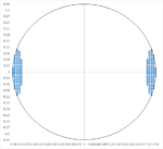
For 0.55 NA systems, the hope has been that single exposure can pattern both horizontal and vertical 22nm pitch features simultaneously, with pupil fill over 20%. However, some 2D features, such as 31 nm pitch staggered contacts/vias (Figure 2), are not conveniently compatible with this exposure, due to the obscuration eliminating the lowest diffracted order [4].
Figure 2. A quasar illumination shape is required for satisfying both 22 nm horizontal and vertical pitches in the layout, but 31 nm staggered features would restrict the illumination further, to below 20% of the pupil.
A smaller portion of the 22 nm pitch quasar illumination such that the lowest diffracted order avoids the obscuration is safe to use, but fills less than 20% of the pupil, again meaning extra condenser absorption and reduced throughput as in the 0.33 NA case. This pattern incompatibility has not featured in prior lithography systems, as they do not have any obscuration. But for the 0.55 NA EUV system, if this staggered 2D pattern needs to be kept along with the horizontal and vertical features, it has to be exposed separately.
Even bigger concerns for single exposure?
22 nm (or smaller) pitch 0.55 NA single exposure will require the use of ultrathin (≤20 nm) resists, due to the reduced depth of focus. For a 20 nm resist thickness, the absorption would go down to 10% for chemically amplified resists (5/um) and a third for metal-oxide resists (20/um), meaning most energy would be absorbed underneath the resist. A limited portion of this energy may be returned to the resist as returning photoelectrons and secondary electrons, since these electrons are, in fact, emitted preferentially parallel to the resist/underlayer interface [5,6] (Figure 3).
Figure 3. At resist thicknesses below 30 nm, most EUV photons (black) are absorbed underneath the resist film (orange), with photoelectrons (red) and secondary electrons (green) emitted largely parallel to the interface. Photoelectron emission is preferentially directed along the electric field direction (purple), with subsequent secondary electron emission preferentially maintaining the photoelectron direction.
EUV exposure thus becomes less energetically efficient as resists grow thinner. Moreover, stochastic effects are aggravated by the reduced absorption. Consequently, multipatterning is expected to be significantly used even for EUV at 3nm. The environmental impact of EUV use therefore should be reconsidered [7].
References
[1] https://semiengineering.com/transistors-reach-tipping-point-at-3nm/
[2] https://www.allaboutcircuits.com/news/world-first-3nm-tapeout-lithography-Cadence-Design-Systems-Imec/
[3] https://semiwiki.com/forum/index.php?threads/nxe-3400c-euv-throughput-vs-dose.13707/
[4] E. van Setten et al., “High NA EUV lithography: Next step in EUV imaging “, Proc. SPIE 10957, 1095709 (2019).
[5] https://www.linkedin.com/pulse/demonstration-dose-driven-photoelectron-spread-euv-resists-chen/; M. Kotera et al., “Extreme Ultraviolet Lithography Simulation by Tracing Photoelectron Trajectories in Resist,” Jpn. J. Appl. Phys. 47, 4944 (2008).
[6] F. Tacoggna, “Secondary Electron Emission Models for PIC Simulations”, https://htx.pppl.gov/exb2018presentations/Friday/2%20Taccogna_SEE.pdf
[7] L-A. Ragnarsson et al., “Environmental Impact of CMOS Logic Technologies,” EDTM 2022.
This article originally appeared in LinkedIn Pulse: EUV’s Pupil Fill and Resist Limitations at 3nm
Also Read:
ASML- US Seeks to Halt DUV China Sales
Obscuration-Induced Pitch Incompatibilities in High-NA EUV Lithography