There are many exciting technologies that are expected to shape the future, the following are some of the technologies that will impact our lives in the coming 5 years at different levels and depth:
Generative AI, also known as generative artificial intelligence, is a type of #AI that is designed to generate new content or data based on a set of input parameters or a sample dataset. This is in contrast to traditional AI, which is designed to analyze and interpret existing data.
There are several different types of generative AI, including generative models, which use machine learning algorithms to learn the underlying patterns and structures in a dataset, and then generate new data based on those patterns; and generative adversarial networks (GANs), which are a type of machine learning model that consists of two neural networks that work together to generate new data.
Generative AI has a wide range of potential applications, including image and video generation, music composition, and natural language processing. It has the potential to revolutionize many industries, including media and entertainment, advertising, and healthcare.
A voice user interface (VUI) is a type of user interface that allows people to interact with devices, applications, or services using voice commands. VUIs are becoming increasingly popular due to their ease of use and the increasing capabilities of natural language processing (NLP) technology, which enables devices to understand and respond to human speech.
VUIs are used in a variety of applications, including smart speakers, virtual assistants, and home automation systems. They allow users to perform tasks or access information simply by speaking to the device, without the need for manual input or navigation.
#VUIs can be designed to understand a wide range of commands and queries, and can be used to control various functions and features, such as setting reminders, playing music, or turning on the lights. They can also be used to provide information and answer questions, such as providing weather updates or answering queries about a particular topic.
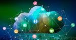
Edge computing is a distributed computing paradigm that brings computing and data storage closer to the devices or users that need it, rather than relying on a central server or cloud-based infrastructure.
In edge computing, data is processed and analyzed at the edge of the network, where it is generated or collected, rather than being sent back to a central location for processing. This can help to reduce latency, improve performance, and increase the scalability of systems that require real-time processing or decision-making.
Edge computing is used in a variety of applications, including the Internet of Things (IoT), where it allows devices to process and analyze data locally, rather than sending it over the network to a central server. It is also used in applications that require low latency, such as video streaming and virtual reality, as well as in industrial and military applications where a central server may not be available.
5G networks use a range of technologies and frequencies to provide coverage, including millimeter wave bands, which are high-frequency bands that can provide very fast data speeds, but have limited range. They also use lower-frequency bands, which can provide wider coverage but lower data speeds.
#5G networks are expected to offer data speeds that are much faster than previous generations of mobile networks, with some experts predicting speeds of up to 10 gigabits per second. They are also expected to offer lower latency, or the time it takes for a signal to be transmitted and received, which is important for applications that require real-time responses, such as video streaming and online gaming.
5G technology is still in the early stages of deployment, and it is expected to roll out gradually over the coming years. It is likely to be used in a variety of applications, including mobile devices, IoT devices, and a wide range of other applications that require fast, reliable connectivity.
A Digital Twin is a virtual representation of a physical object or system. It is created by using data and sensors to monitor the performance and characteristics of the physical object or system, and using this data to create a digital model that reflects the current state and behavior of the physical object or system.
Digital twins can be used in a variety of applications, including manufacturing, healthcare, and transportation. In manufacturing, for example, a digital twin can be used to simulate the performance of a production line or equipment, allowing manufacturers to optimize their operations and identify potential issues before they occur. In healthcare, digital twins can be used to model the body or specific organs, allowing doctors to better understand the patient’s condition and plan treatment.
Digital twins are created using a combination of sensors, data analytics, and machine learning techniques. They can be used to visualize and analyze the behavior of the physical object or system, and can be used to optimize performance, identify issues, and make decisions about how to improve the physical object or system.
Quantum Computers are different from classical computers, which use bits to store and process information. Quantum computers can perform certain types of calculations much faster than classical computers, and are able to solve certain problems that are beyond the capabilities of classical computers.
One of the key benefits of quantum computers is their ability to perform calculations that involve a large number of variables simultaneously. This makes them particularly well-suited for tasks such as optimization, machine learning, and data analysis. They are also able to perform certain types of encryption and decryption much more quickly than classical computers.
Quantum computing is still in the early stages of development, and there are many challenges to overcome before it becomes a practical technology. However, it has the potential to revolutionize a wide range of industries, and is likely to play an increasingly important role in the future.
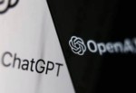
A Chat Bot is a type of software that is designed to engage in conversation with human users through a chat interface. Chat bots are typically used to provide information, answer questions, or perform tasks for users. They can be accessed through a variety of platforms, including messaging apps, websites, and social media.
There are several different types of chat bots, including rule-based chat bots, which are designed to respond to specific commands or queries; and artificial intelligence (AI)-powered chat bots, which use natural language processing (NLP) to understand and respond to more complex or open-ended queries for example #ChatGPT.
Chat bots are commonly used in customer service, where they can handle routine inquiries and help customers resolve simple issues without the need for human intervention. They are also used in marketing, where they can help businesses to connect with customers and provide information about products and services.
XR is a term that is used to refer to a range of technologies that enable immersive experiences, including virtual reality (VR), augmented reality (AR), and mixed reality (MR).
Virtual reality (VR) is a technology that allows users to experience a simulated environment as if they were physically present in that environment. VR is typically experienced through the use of a headset, which allows users to see and hear the virtual environment, and sometimes also to interact with it using handheld controllers or other input devices.
Augmented reality (AR) is a technology that allows users to see virtual elements superimposed on their view of the real world. #AR is often experienced through the use of a smartphone or other device with a camera, which captures the user’s surroundings and displays virtual elements on top of the real-world view.
Mixed reality (MR) is a technology that combines elements of both VR and AR, allowing users to interact with virtual elements in the real world. #MR typically requires the use of specialized hardware, such as a headset with a built-in camera, which captures the user’s surroundings and allows virtual elements to be placed within the real-world environment.
Distributed ledger technology (DLT) is a type of database that is distributed across a network of computers, rather than being stored in a central location. It allows multiple parties to share and update a single, tamper-evident record of transactions or other data, without the need for a central authority to oversee the process.
One of the most well-known examples of #DLT is the blockchain, which is a decentralized, distributed ledger that is used to record and verify transactions in a secure and transparent manner. Other examples of DLT include distributed databases, peer-to-peer networks, and consensus-based systems.
DLT has a wide range of potential applications, including financial transactions, supply chain management, and identity verification. It is also being explored for use in the development of new products and services, such as smart contracts and decentralized applications (dApps).
The Internet of Things (IoT) is a network of connected devices that are able to communicate and exchange data with each other. These devices can range from simple sensors and actuators to more complex devices such as smart thermostats and appliances.
The #IoT is made possible by the widespread availability of broadband internet, as well as the development of low-cost sensors and other technologies that enable devices to be connected to the internet. These devices are often equipped with sensors that allow them to gather data about their environment or their own operation, and are able to communicate this data to other devices or systems.
The IoT has the potential to transform many aspects of our lives, including how we live and work. For example, smart home systems that use IoT technology can allow users to control and monitor their home appliances and systems remotely, and can provide alerts and notifications about potential issues. The IoT is also expected to play a significant role in the development of smart cities, which are urban environments that use technology to improve the quality of life for residents.
Ahmed Banafa, Author the Books:
Secure and Smart Internet of Things (IoT) Using Blockchain and AI
Blockchain Technology and Applications
Quantum Computing
References
1. “Secure and Smart IoT Using Blockchain and AI “ Book by Prof. Ahmed Banafa
2. “Blockchain Technology and Applications “ Book by Prof. Ahmed Banafa
3. ChatGPT (Chat of Generative Pre-training Transformer)
Also Read:
CES 2023 and all things cycling
9 Trends of IoT in 2023
Microchips in Humans: Consumer-Friendly App, or New Frontier in Surveillance?