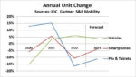
Banner 800x100 0810

Radiodays Europe: Emotional Keynote

Radiodays Europe: Emotional Keynote
by Roger C. Lanctot on 05-21-2022 at 6:00 am

Radiodays Europe Emotional Keynote

One doesn’t expect to get emotional at the kickoff keynote for an industry event, but Radiodays Europe 22 flipped the script with live music and a bulletin from Ukrainian broadcasters beamed in from a bunker in Ukraine. The bunker broadcast followed speeches from Swedish and Finnish broadcasting executives including Cille Benko, director general and CEO of Swedish Radio.

Benko noted in her comments that the local broadcaster in Sweden went live eight minutes after the start of Russia’s invasion at 4 a.m., Feb. 24th, with a 48-hour live broadcast of bulletins from the front. Benko noted a boost of up to half a million radio listeners out of a total population of 10M reflecting the power of live radio broadcasts in such emergency circumstances.

Benko’s insight was made even more powerful by the fact that both print and television media have seen a steady audience erosion. In the current environment, radio is shining as a source of immediate and trusted information.

The choice of Malmo, Sweden, for the Radiodays Europe 22 event was particularly prescient given the announced intent of Sweden and Finland to join the North Atlantic Treaty Organization (NATO) in the wake of the Ukrainian invasion. Benko gave a strong boost to the notion of radio as a live and local medium, calling for the broadcasters in attendance to leverage technology for more content creation outside the studio and for taking advantage of podcasts and on-demand engagement with listeners.

Far from being passe or secondary to video content, Benko pronounced audio as ascendant and with decided advantages over other forms of content. Helsinki-based Stefan Moller, President of the Association of European Radio, added to the emotional undercurrent with his own comments regarding the urgency of radio’s role in the current environment.

But the most powerful message came from the sub-terranean Ukrainians, Andriy Tarano and Dmytro Khorkin, representing Ukrainian Public Broadcasting, who joined the event via video to thank their international supporters and describe their ongoing efforts to broadcast via all means available including mobile apps. They also noted that only AM broadcasts were currently available in Mariupol.

Radio advocates have long noted radio’s ability to endure and deliver critical information in times of crisis such as earthquakes and hurricanes, when cellular and Internet communications are often knocked offline. The Radiodays Europe keynote highlighted the extent to which political events can reshape the media environment and alter the conventional wisdom governing public perceptions. There are few positive messages to be taken from the disastrous invasion of Ukraine by Russia, but one such message is the enduring power and relevance of broadcast radio.

SOURCE: Dmytro Khorkin and Andriy Taranov of Public Broadcasting Company of Ukraine speaking via video to Radiodays Europe 22 opening session in Malmo, Sweden.

Also Read:

Why Traceability Now? Blame Custom SoC Demand

Taxis Don’t Have a Prayer

The Jig is Up for Car Data Brokers


Podcast EP81: The Future of Neural Processing with Quadric’s Steve Roddy

Podcast EP81: The Future of Neural Processing with Quadric’s Steve Roddy
by Daniel Nenni on 05-20-2022 at 10:00 am

Dan is joined by Steve Roddy, chief marketing officer of Quadric, a leading processor technology intellectual property (IP) licensor. Roddy brings more than 30 years of marketing and product management expertise across the machine learning (ML), neural network processor (NPU), microprocessor, digital signal processor (DSP) and semiconductor IP industries.

Dan and Steve discuss the current state of AI deployment, today and tomorrow. Steve provides an overview of the products being developed by Quadric – how they fit today and a bit about where the company will take the industry tomorrow.

The views, thoughts, and opinions expressed in these podcasts belong solely to the speaker, and not to the speaker’s employer, organization, committee or any other group or individual.


Intel to present Intel 4 process at the VLSI Technology Symposium

Intel to present Intel 4 process at the VLSI Technology Symposium
by Scotten Jones on 05-20-2022 at 8:00 am

VLSI Symposium 2022 SemiWiki 1

The VLSI Symposium on Technology & Circuits will be held in Hawaii from June 12th to June 17th. You can register for the conference here.

The tip sheet for the conference has been released and one thing that caught my eye is some data from the Intel 4 paper that Intel will be presenting at the conference.

Intel’s old roadmap had 14nm, 10nm and then 7nm processes with 7nm being the first EUV based process and providing a 2x density improvement over 10nm. Intel eventually updated their roadmap to be more consistent with the numbering scheme used by Samsung and TSMC.

Intel has several versions of their 10nm process, the original version (or two) and then the super fin and enhanced super fin versions. Under the new scheme Intel’s 10nm enhanced super fin version became Intel 7, and the former 7nm process was replaced by Intel 4.

Intel 10nm has a transistor density of approximately 100 million transistors per millimeter squared, that is consistent with the density of Samsung and TSMC’s 7nm processes. I also believe Intel’s enhanced super fin process has performance as good or better than either of the foundry 7nm processes. Renaming Intel’s 10nm enhanced super fin to Intel 7 is therefore a designation more consistent with the foundry numbers.

When Intel announced Intel 4 they said it would provide a 20% performance per watt improvement and a significant density improvement but they didn’t provide a number. I thought this might mean they were relaxing the 2x density improvement, but the tip sheet disclosed that it is still 2x relative to 7nm. This would put the density between TSMC’s 5nm and 3nm processes, so Intel 4 is once again a name consistent with the foundry naming convention.

Does this mean Intel 4 will be around 200 million transistors per millimeter squared? This is actually a less straight forward question than you might think. When companies disclose dimensions for their processes, they often disclose values that are smaller than what are seen in standard cells. For example, TSMC says their 7nm process has a 54nm contacted poly pitch (CPP) but our strategic partner TechInsights measured 57nm in standard cells on actual designs. When we characterize a process what we have standardized on is using the densest standard cell seen on an actual part (once parts are available for analysis). TechInsights first saw 10nm Intel parts in 2018 in what TechInsights referred to as generation 1.

Generation 1 had a 54nm CPP consistent with what Intel claims. TechInsights saw generation 2 parts in 2019 that also had a 54nm CPP (the fins were taller than generation 1 suggesting is was a new generation). When Intel introduced the super fin version of 10nm they added an optional 60nm CPP for high performance cells. TechInsights analyzed these parts (generation 3) and saw both 54nm and 60nm CPP cells. Based on our convention this still works out to approximately 100 million transistor per millimeter squared. Where this gets interesting is the recent analysis TechInsights did on the enhanced super fin process (10nm generation 4, now known as Intel 7). This process also has an optional 60nm CPP, but what is interesting is in the standard cell logic, TechInsights only saw the 60nm CPP, no 54nm CPP and a taller track height. This results in a calculated density of approximately 60 million transistors per millimeter squared. So is Intel 4 going to be 200 million transistors per millimeter squared (100 x 2) or 120 million transistor per millimeter squared (60 x 2)?

My belief is it will be 200 million transistor per millimeter squared but it will be interesting to see how much of an actual design utilizes that density.

There is more data in the tip sheet to help answer this. The tip sheet discloses that the CPP is 50nm and the minimum metal pitch is 30nm. Current leading-edge processes all use a single diffusion break so we will assume that here as well. The only remaining question is track height, if I assume a 1 fin per cell 5-track cell then the density is right around 200 million transistors per millimeter squared. A single fin cell would likely require aggressive performance enhancements to meet Intel’s performance requirements, there might also be other design-technology-co-optimization in the process. A 5-track cell is possible for FinFETs without Buried Power Rail so this could be a solution.

It will be interesting to see what other data is included in the full paper. The fact that Intel is giving this paper does add additional weight to Intel being on track to introduce Intel 4 late this year.

SemiWiki blogger Tom Dillinger will be attending the event so you can read more from him after the event.

Also read:

The Lost Opportunity for 450mm

Intel and the EUV Shortage

Can Intel Catch TSMC in 2025?


CEO Interview: Vaysh Kewada of Salience Labs

CEO Interview: Vaysh Kewada of Salience Labs
by Daniel Nenni on 05-20-2022 at 6:00 am

Salience Vaysh Kewada

Vaysh Kewada is cofounder and CEO at Salience Labs, a company developing an ultra high-speed multi-chip processor that packages a photonics chip together with standard electronics to enable exascale AI. Salience is funded by Oxford Sciences Enterprise, Cambridge Innovation Capital, Arm-backed Deeptech Labs, former Dialog Semiconductor CEO Jalal Bagherli and former Temasek board member Yew Lin Goh. Prior to launching Salience Labs, Vaysh worked at Oxford Sciences Enterprises, a $745M VC fund focused on deep-tech investments. Prior to that, she was a management consultant at McKinsey & Company. Vaysh holds an undergraduate and Masters degree in Physics from Imperial College London, where her thesis focussed on genetic algorithms.

Tell us about Salience Labs?
Salience Labs was spun out of Oxford and Münster universities in 2021 to commercialise an ultra-high-speed multi-chip processor that packages a photonics chip together with standard electronics. By using light to execute operations, we can deliver massively parallel processing performance – bringing ultra-high speed compute to a wide array of new and existing AI processes and applications.

The compute requirements of AI double every 3-4 months, as the world needs ever-faster chips to grow AI capability. The current semiconductor industry can’t keep pace with this demand. What’s required now is not further incremental innovations on transistor technology. If we are to realise the tremendous potential of AI, nothing short of a paradigm shift in the way we compute will do. One that delivers an immediate step change in performance and speed, while also offering a long-term future roadmap of scaling improvements.

Multi-chip processors – ones that package together several platform technologies – is that step-change, allowing us to package electronics together with silicon photonics, and to move compute from electronics to the realm of light. By using light to execute operations, it’s possible to achieve massively parallel performance and deliver high throughput, low latency matrix maths – at the root of almost all AI applications. And it’s possible to do this with clocking speeds in the 10s of GHz – where currently the limitation of even the most cutting-edge chips is just 2-3 GHz.

Why was Salience Labs founded?
Salience was founded with the vision of creating an exa-scale processor, by packaging a photonics chip together with standard electronics. The technology is based on decades of research at University of Oxford and Münster University in Germany.

The key inventors and researchers of the technology: Professor Wolfram Pernice, Professor Harish Bhaskaran and Dr. Johannes Feldmann, are co-founders in the company, giving Salience Labs significant depth of knowledge in this field.

What makes Salience Labs technology unique?
While other photonic chip companies execute operations in the phase of light, we use a proprietary amplitude-based approach to photonics, resulting in modular, dense computing chips clocking at 10’s of GHz. It also allows for high levels of parallelization, by using different wavelengths of light to send many calculations through the chip. Salience uses a multi-chip design, with the photonic processing mapping directly on top of the Static Random Access Memory (SRAM). This novel ‘on-memory compute’ architecture allows for the fast compute in the photonic domain to be fully utilized, delivering an exceedingly dense computing chip without having to scale the photonics chip to large sizes. This architecture can be adapted to the application-specific requirements of different market verticals, making it ideal for realising AI inference use-cases in communications, robotics, vision systems, healthcare and other data workloads.

How has the company evolved since you founded it?
We originally spun-out of the University of Oxford and the University of Münster in 2021 and have just closed our seed round of $11.5 million from a number of leading VCs including Cambridge Innovation Capital, Oxford Science Enterprises and Arm-backed Deeptech Labs participating, plus some leading names in the semiconductor industry including former CEO of Dialog Semiconductor Jalal Bagherli and Yew Lin Goh. Since closing our seed round, our focus has been on the tape out of our next test chip, developing our software models and packaging solutions. We are also building relationships with customers across a range of market verticals.

You are participating in the Silicon Catalyst incubator programme. What has been the impact on the business?
We joined the Silicon Catalyst programme in 2021, right after spinning out from Münster and Oxford Universities. The greatest benefit is the access it gives us to advisors – individuals who have made a significant impact on the global semiconductor industry. In fact, we met our chairman Dan Armburst through the programme, who is a Silicon Catalyst Co-founder and Board Director. Through those advisors, we gained highly valuable commercial introductions to foundries, IP providers, and EDA providers at a very early-stage of the company. It has given Salience Labs’ a commercial jump start. For example, we’ve just closed our seed round but we’re already working with production level foundries on the fabrication of our next test chip. Silicon Catalyst has been a tremendous accelerator for our business.

What can we hope to see from Salience Labs in the future?
We’re at a very interesting point in time where the industry is recognising the potential of multi-chip processors to solve the tremendous processing bottleneck currently hampering AI growth. Salience Labs’ technology has the potential for breakthrough performance and power capability beyond what the established CMOS roadmap offers. We’re talking to customers across a range of market verticals who are excited about the performance improvements silicon photonics will offer and the new AI processes and applications this will enable. We welcome any additional approaches from potential customers who are interested in understanding the capabilities of silicon photonics.

Also read:

CEO Interview: Chuck Gershman of Owl AI

CEO Interviews: Dr Ali El Kaafarani of PQShield

CEO Interview: Dr. Robert Giterman of RAAAM Memory Technologies


Joseph Sawicki of Siemens EDA at User2User

Joseph Sawicki of Siemens EDA at User2User
by Daniel Payne on 05-19-2022 at 10:00 am

Joseph Sawicki

I attended the annual user group meeting called User2User in Santa Clara this year, hosted by Siemens EDA, with 51 presentations by customers in 11 tracks, and keynotes during each lunch hour from semiconductor executives. Joseph Sawicki, Executive VP, IC Segment, at Siemens EDA presented on a Tuesday, along with Prashant Varshney, Microsoft, and Mahesh Tirupattur, Analog Bits. This blog focuses on what I heard from Mr. Sawicki.

The host Harry Foster said that each keynote was like a Ted Talk, and they certainly lived up to that.  Joseph’s topic was, From ICs to Systems – New Opportunities for the Semiconductor Industry. Digitalization is driving across all industries: Aerospace, auto, consumer, electronics and semi, energy, heavy, medical, marine, industrial.

There is now a pervasive AI enablement; in sensors, edge computing, 5G/wireless comm, cloud and data centers. The share of semiconductors in electronic systems from the time period of 1992- 2014 was 16%, but now has grown to about 24%, and predictions show that electronic systems will reach $3.2T revenue by 2025, so quite the growth market.

Systems companies are becoming IC designers, and there are many examples: Apple, Amazon, Google, ZTE, Tesla, Bosch, Huawei, Facebook. Foundries have seen the Systems companies grow from just 1% of revenue in 2011, now to 21% in 2021, that’s big growth and Apple has become the number one customer of TSMC. At the Hot Chips conference in 2006 just 16% of the accepted papers came from systems companies, while by 2021 that number had grown to 33% of the papers. So the systems companies are driving innovation in chip design.

Consider the history of Apple, their first 64 bit application processor was introduced way back in 2013, but why do that? Even in 2022 you still don’t need 64 bits for the larger RAM address space. The answer was for performance, an ARM core can run either in 32 or 64 bit modes, and running in 64 bit mode has 31% better performance.

Apple A7, Source: Chipworks

There’s some new trends in automotive, Cars as a Service, where Volvo plans to reach 50% of their revenue through services by 2025. Tesla provides OTA (Over The Air) update services and new feature upgrades, adding revenue after the initial sales. Gartner Group reports that half of the top 10 auto OEMS will be designing some of their own chips by 2025, with 7 of 10 already announced by 2021. Ford and Globalfoundries will partner in IC design in order to smooth out the supply chain issues that have hurt the industry since the COVID pandemic started in 2020.

The gradual electrification of vehicles is a major driver of new IC design starts, and the semiconductor revenue per vehicle should reach $500 per car by 2028, so that’s a $24B market. 5G communication will be important to automotive for OTA updates and services, and is growing 3X per year.

The total number of sensors connected to Internet was 1.6B in 2015, exploding in growth to 29.6B sensors by 2025, so that’s big growth of video, data, and data center.

Source: IC Insights

Semiconductor content inside of Data Centers is growing to $242B by 2030, which is a 14% CAGR, per IBS, Sept. 2021.

With all of these demands on semiconductors in growth markets, how is our industry going to meet the them? Joseph summarized that there are three trends to meet demand:

  1. Technology scaling – new nodes and 3D IC
  2. Design scaling – silicon integration
  3. System scaling – digital twin, verifying a device against spec and the full SW stack with apps

For technology scaling we can look at Moore’s Law, it’s not quite dead, because look at the A-series from Apple over time. From 2013 to 2021, we saw transistor counts growing from 1 billion to 15 billion, so it’s still scaling pretty well at 15X. Dennard Scaling has died – so clock cycle rates are not improving by 16X over that 8 year time frame. Looking at single core CPU performance , the Geekbench scores have ranged from 269 to 1734, so it’s growing on track. Even the foundries have another 8 years to grow process technology in their road maps.

Monolithic integration is growing, yes, but 3D design is coming along too, combined with innovative packaging. System in a Package is a new trend. System and design technology co-optimization is needed to be successful.

On design scaling there are charts that claim that 7nm designs cost $280M, but is that reality? That number sounds too big, yet the trend line is true, as small nodes drive up the design and verification costs. One method to counter that increase in costs is to move from RTL up to C level design for systems designs. Consider the example of NVIDIA, where a small team of just 10 engineers in 6 months taped out a new chip for deep learning inference accelerator by using C++ with an HLS (High Level Synthesis) methodology, as reported at Hot Chips in Aug 2019. Google is another systems company using HLS to help manage SoC design costs.

For System Scaling the idea is to create a true digital twin. One example of digital twin is something called PAVE360 – it’s a way to validate automotive models with traffic, people and vehicles. You can run this digital twin in order to validate virtual models, or run SW for your ADAS system, to model power, vehicle modeling (power train, chassis, seating, effect of road on occupants). It’s a way to safely validate before production starts.

The final topic was lifecycle management, so consider a data center with hundreds of thousands of blades, where you can actually monitor all of the blades in real time, debug any reliability issues in that data center, and you can analyze all of the embedded sensor data, literally tracking the health of the data center.

Summary

A trillion dollar semiconductor industry is shortly approaching us, so this is an exciting time to be part of the EDA industry which enables all of this growth, as systems designers are taking on new design starts, AI is everywhere, electrification of vehicles continues, and digital twins are being adopted. The mood of the presentation was quite upbeat, and well received by the audience.

Related Blogs


TSMC N3 will be a Record Setting Node!

TSMC N3 will be a Record Setting Node!
by Daniel Nenni on 05-19-2022 at 6:00 am

waferr007 2518 Q9Wf 0

With the TSMC Technical Symposium coming next month there is quite a bit of excitement inside the fabless semiconductor ecosystem. Not only will TSMC give an update on N3, we should also hear details of the upcoming N2 process.

Hopefully TSMC will again share the number of tape-outs confirmed for their latest process node. Given what I have heard inside the ecosystem, N3 tape-outs will be at a record setting number. Not only has Intel joined TSMC for multi-product high volume N3 production, it has been reported that Qualcomm and Nvidia will also use N3 for their leading edge SoCs and GPUs. In fact, it would be easier to list the companies that will not use TSMC for 3nm but at this point I don’t know of any. It is very clear that TSMC has won the FinFET battle by a very large margin, absolutely.

“The most outstanding news of TSMC in 2021 was the success in attracting more new business from Intel, while being able to maintain great relationships with existing customers such as AMD, Qualcomm and Apple. With its 3 nm N3 entering volume production later in 2022 with good yield and 2 nm N2 development being on track for volume production in 2025, TSMC is expected to continue its technology leadership to support its customer innovation and growth. Thanks to the demand of bleeding-edge technologies, TSMC’s foundry leadership position seems to have become even more concrete in recent years.”

Samuel Wang, analyst with Gartner, from their recent analyst report: “Market Share Analysis: Semiconductor Foundry Services, Worldwide, 2021” that went live on May 9, 2022.

Now that live events have started up again in Silicon Valley the information flow inside the semiconductor ecosystem has returned to pre pandemic levels. I have attended (6) live semiconductor events thus far in 2022 and have several more to go before the biggest foundry event The 2022 TSMC Technology Symposium which kicks off at the Santa Clara Convention Center on June 16 followed by events in Europe (6/20), China (6/30), and Taiwan (6/30).

SemiWiki has covered the TSMC events for the past 11 years and we will have bloggers attending this year as well. This is the number one networking event for TSMC customers, partners, and suppliers so I can assure you there will be a lot to write about.

Here is the most recent update on technology development from TSMC:

  • TSMC’s 3nm technology development is on track with good progress, and the company has developed complete platform support for HPC and smartphone applications. TSMC N3 is entering volume production in the second half of 2022, with good yield.
  • TSMC N3E will further extend its 3nm family, with enhanced performance, power, and yield. The Company also observed a high level of customer engagement at N3E, and the volume production for N3E is scheduled for one year after N3
  • Faced with the continuous challenge to significantly scale up semiconductor computing power, TSMC has focused its R&D efforts on contributing to customers’ product success by offering leading-edge technologies and design solutions. In 2021, the company started risk production of 3nm technology, the 6th generation platform to make use of 3D transistors, while continuing the development of 2nm, the leading-edge technology in the semiconductor industry today. Furthermore, the company’s research efforts pushed forward with exploratory studies for nodes beyond 2nm. TSMC’s 2nm technology has entered the technology development phase in 2021, with development being on track for volume production in 2025.

TSMC also introduced N4P process in October 2021, a performance-focused enhancement of the 5nm technology platform. N4P delivers an 11% performance boost over the original N5 technology and a 6% boost over N4. Compared to N5, N4P will also deliver a 22% improvement in power efficiency as well as a 6% improvement in transistor density.

TSMC introduced N4X process technology at the end of 2021, which offers a performance boost of up to 15% over N5, or up to 4% over the even faster N4P at 1.2 volt. N4X can achieve drive voltages beyond 1.2 volt and deliver additional performance. TSMC expects N4X to enter risk production by the first half of 2023. With N5, N4X, N4P, and N3/N3E, TSMC customers will have multiple and compelling choices for power, performance, area, and cost for their products.

Bottom line: This will be one of the more exciting TSMC Technical Symposiums. TSMC N2 has been under NDA while the IDM foundries have been leaking details about their upcoming 2nm processes. This is a classic marketing move, when you don’t have a competing product today, talk about tomorrow.

One thing we should all remember is that all of the leading semiconductor companies, with the exception of Samsung, are collaborating with TSMC. The TSMC ecosystem consists of 100s of customers, partners, and suppliers and it is like no other. If you think another foundry will have a higher yielding 2nm process that can support a wide range of products you would be wrong.

Also read:

Can Intel Catch TSMC in 2025?

TSMC’s Reliability Ecosystem

Self-Aligned Via Process Development for Beyond the 3nm Node


Webinar – 112 Gbps PAM4 Implementation with Real-World Case Studies

Webinar – 112 Gbps PAM4 Implementation with Real-World Case Studies
by Mike Gianfagna on 05-18-2022 at 10:00 am

Webinar – 112 Gbps PAM4 Implementation with Real World Case Studies

Are 112G PAM4 channels in one of your current or future designs? If you’re focusing on advanced products, the answer is likely YES. Design of these channels is quite challenging. Silicon design, SerDes, PCB traces, and interconnect all need to be balanced to achieve success. As they say, getting there is half the fun. An upcoming webinar tackles these challenges head-on, with no less than six real-world case studies to show how it’s done. The speakers are world-class, as are their companies. This is where you find the tricks of the trade that save you time, and perhaps save your project. The webinar is in early June, so there’s plenty of time to register. Read on if you want to learn more about 112 Gbps PAM4 implementation with real-world case studies.

The presenters, and their companies

Clint Walker

Clint Walker, VP of marketing at Alphawave IP. Clint has over 24 years of semiconductor experience. Before moving to Alphawave IP, Clint was a principal engineer and senior director at Intel where he worked for 22 years focused on high-speed I/O systems and circuit architecture. Clint has participated and contributed to JEDEC DDR, PCI-SIG, and IEEE 802.3 standards development and is the former chair of USB3.0 Electrical Work Group.

Alphawave IP is a global leader in high-speed connectivity for the world’s technology infrastructure. Its IP solutions meet the needs of global tier-one customers in data centers, compute, networking, AI, 5G, autonomous vehicles, and storage. Its mission is to focus on the hardest-to-solve connectivity challenges.  You can learn more about Alphawave IP on SemiWiki here.

Matt Burns

Matthew Burns, technical marketing manager at Samtec. Matt develops go-to-market strategies for Samtec’s Silicon to Silicon solutions. Over the course of 20+ years, he has been a leader in design, technical sales and marketing in the telecommunications, medical and electronic components industries. He holds a B.S. in Electrical Engineering from Penn State University.

Founded in 1976, Samtec is a privately held, global manufacturer of a broad line of electronic interconnect solutions, including High-Speed Board-to-Board, High-Speed Cables, Mid-Board and Panel Optics, Precision RF, Flexible Stacking, and Micro/Rugged components and cables. Samtec Technology Centers are dedicated to developing and advancing solutions to optimize both the performance and cost of a system from the bare die to an interface 100 meters away. You can learn more about Samtec on SemiWiki here.

What you’ll see

The six real-world test cases include Samtec’s 112 Gbps PAM4 connector systems. They include board-to-board connector sets, as well as two Samtec Flyover® cable systems. One is a mid-board to cable backplane configuration, and the other is mid-board to front panel. These cable systems are emulating real-world data center system architectures.

Each board also has four Alphawave AlphaCORE Multi-Standard SerDes. For each connector set, the Alphawave SerDes is transmitting 112 Gbps PAM4 PRBS data, and Samtec is receiving and analyzing the signal performance on the other board.

The six connector systems are on two boards. The two boards are communicating bidirectionally at 112 Gbps PAM4. All of the cable assemblies use Samtec Eye Speed® ultra-low skew twinax. The tight coupling between signal conductors in this co-extruded cable, made by Samtec, improves signal integrity performance, bandwidth, and reach.

These configurations are using cutting-edge, 112 Gbps PAM4 data. The results presented in the webinar are spectacular. If high-performance channels are in your future, you really need to see this. Precision, high-performance SerDes, advanced channel design and aggressive signal integrity methods all play a role here.

To learn more

The results presented in this webinar will wow you. These are real, live physical systems, not simulations. The implementations presented will give you courage to embark on your next close-to-impossible design project. Those are the best kind.

The webinar will be broadcast on Thursday, June 2, 2022, from 11:00 AM – 12:00 PM EDT. You can view the replay here. Now you know how to become an expert on 112 Gbps PAM4 implementation with real-world case studies.


Podcast EP80: The Future of Silicon Photonics with Dr. Anthony J. Yu

Podcast EP80: The Future of Silicon Photonics with Dr. Anthony J. Yu
by Daniel Nenni on 05-18-2022 at 8:00 am

Dan is joined by Dr. Anthony J. Yu, vice president of the Computing and Wired Infrastructure (CWI) Business Unit at GlobalFoundries (GF), where he is responsible for providing differentiated photonic manufacturing services and solutions to clients across multiple industries. Prior to being named VP of CWI, Dr. Yu was vice president of GF’s Aerospace and Defense Business Unit. Before joining GF, he held multiple executive positions at IBM, including vice president of Semiconductor Technology for Engineering and Technology Services.

Dan and Anthony explore the applications of silicon photonics, both today and what will be coming soon. The applications, both current and future as well as the players, current and emerging are all discussed. The impact of this technology is substantial.

The views, thoughts, and opinions expressed in these podcasts belong solely to the speaker, and not to the speaker’s employer, organization, committee or any other group or individual.


Why Traceability Now? Blame Custom SoC Demand

Why Traceability Now? Blame Custom SoC Demand
by Bernard Murphy on 05-18-2022 at 6:00 am

Traceability abstract min

In the SoC world, we can’t believe our good luck. Every product maker now wants bespoke silicon solutions with the most advanced AI, communications, SLAM, etc. Which is fantastic for business, but this level of demand also drags us into a new level of accountability, especially in requirements traceability. Time was that only software teams had to worry about the headaches of traceability. Hardware platforms used branded devices such as microprocessors with proven track records; variability at most was in board design. However, in a scramble for functional differentiation at acceptable power and cost, product builders now demand both custom software and hardware stacks. Inevitably, traceability then crosses into hardware. Which is why SoC developers are now hearing about this topic.

A review

Traceability is a concept which mandates tracking between initial requirements and implementation as represented in logic design, verification and documentation. This method is used widely in logistics, food processing and many other domains. In electronic systems development, system builders first pushed traceability to control compliance in software development and verification, and more recently into SoC design as well. This level of tracking is active already in safety-critical automotive, aerospace and medical markets. Expect to see similar moves around security-sensitive products also.

An enforceable system must be based on structured requirements rather than unstructured natural language specifications. In support of this objective, systems designers have adopted tools like IBM DOORS and Jama Connect. Using such tools, they can describe hierarchically and concisely what they expect to satisfy their objective for the complete system. A supplier architect will typically further elaborate a subset of these requirements applicable to the supplier’s deliverable. Leveraging prior understanding of their own organization’s products and strengths. Further elaboration is possible inside subsystems.

Top-level requirements are decomposed hierarchically, concise at each level, simplifying locating and checking correspondence between a requirement and its implementation. This structure also makes it easy to isolate–if something went wrong–where and why it went wrong. Was it a problem in software, a sensor or one of multiple SoCs? Maybe there was a bug in the memory map? Requirements systems provide a system designer the means to pin down a possible cause without having to read through countless manuals written by multiple suppliers, with the imprecision of natural language. And without having to depend on appeals to trust from suppliers.

Entry-level traceability support

The simplest solution for traceability is a traceability matrix. This is typically a spreadsheet, listing one requirement per row with collateral information (e.g., related files and line numbers) in columns. Spreadsheets can be organized hierarchically and can become quite large and sophisticated.

Manual solutions like this are an obvious starting point but quickly run out of gas. Tracking 100 requirements isn’t a problem. Tracking 10,000 across multiple design, verification and documentation teams would be a huge problem without some level of semantic connection between the spreadsheet, design, test and documentation data. From system developers to SoC architects, translating higher-level requirements to lower-level requirements is a manual step; spreadsheets won’t catch mistakes at these transitions. What happens if a designer makes what seems a harmless change, without being aware of some dependency in another spreadsheet? Can the product maker see the disconnect or will they only trip over it when they run their application software and find it doesn’t work?

There isn’t an infallible answer to these questions, but there is a better answer than spreadsheets. That’s where Harmony Trace™ from Arteris IP comes in.

Professional traceability support

Clearly, a professional solution must support semantically aware connections between requirements and all aspects of the design implementation. Some of these will be derivable connections, given sufficient understanding of the design. In modern SoC design, that generally means down to the IP level. Others will require expert design understanding of system objectives. Generally, the majority will be derivable from a sufficiently structured starting point; think of memory map and register map detail as examples.

Semantically Aware SoC Traceability

These data and traceability connections should remain current as the design evolves, which requires that they should be semantically aware. Traceability can’t simply be to design files and line numbers. If an IP or an address offset changes, that detail should track automatically in traceability without need for designer updates to keep links current.

The link should be bidirectional. Requirements evolve through improved understanding or though necessary updates at the OEM level. Such changes should trickle down, automatically flagging affected design teams. Conversely, if a designer, verifier or documentation writer makes a change on an artifact within the scope of a requirement but on which the requirement is silent, perhaps the system designer should be notified anyway. Maybe that change is safe, maybe not?

There is great opportunity for SoC design organizations but that opportunity comes with more accountability. In being able to prove they built what they were told to build, down to a quite fine level of detail. Arteris IP has a solution for those design teams.


Meet Kandou’s Frank Lavety, Behind the Scenes Point Person for Timely Product Delivery

Meet Kandou’s Frank Lavety, Behind the Scenes Point Person for Timely Product Delivery
by Lauro Rizzatti on 05-17-2022 at 10:00 am

Frank Lavety

I learned about Kandou a year ago and liked what I heard, as should anyone who wants higher res displays and faster downloads from their electronic devices. I’ve been tracking Kandou since and believe it’s living up to its goal to be the undisputed innovator in high-speed, energy-efficient chip-to-chip link solutions to improve the way the world connects and communicates.

My blog last year looked at Kandou’s Matterhorn USB-C multiprotocol retimers with USB4 support. Two variations of Matterhorn, named for the famous Alps Mountain, are already adopted and successfully implemented by OEMs and ODMs developing mobile and desktop PCs. Matterhorn often overshadows Kandou’s equally impressive Chord signaling technologies optimized for high-speed, ultra-low power chiplet and chip-to-chip interconnects delivered as blocks of IP.

Recently, I chatted with Frank Lavety, Kandou’s General Manager and point person behind the scenes ensuring timely delivery of its entire product line. He recently described to me how USB4, the latest USB standard, will do even more to help quench our thirst for information. And noted as an aside, with a worldwide workforce, Frank said it’s nothing short of remarkable that Kandou’s interconnections worked efficiently and with little productivity impact in a pandemic scenario few of us imagined.

Frank joined Kandou in 2018 as VP Operations initially responsible for building Kandou’s fabless manufacturing operations and in 2019 assumed the role of General Manager, leading engineering, manufacturing and the commercialization of Kandou’s Matterhorn product family.

Here is a condensed version of our conversation.

Q: Frank, tell us about your background.

A: After graduating from University, I spent seven years with the medical device manufacturer Haemonetics Corporation, where I learned so much about high-quality, cost-efficient manufacturing. After finishing my MBA, I returned to Scotland from Boston, joining Wolfson Microelectronics in 2001, a fabless semiconductor start-up based in Edinburgh. Wolfson successfully IPO’d on the FTSE in 2003, eventually reaching a market cap of more than $1.5 billion.

During my 10 years at Wolfson, I established global manufacturing operations to support annual revenues in excess of $230 million. As VP Operations, shipped billions of mixed-signal ICs to the world’s largest consumer electronics brands, establishing Wolfson as a world leader in audio technologies.

In 2012, I was looking for a new technology challenge and joined Adlens Ltd., an Oxford University (Oxford, U.K.) spin out developing adaptive lens technologies used in eyewear and AR/VR applications, where I was COO and CEO before joining Kandou two years ago.

What attracted you to Kandou?

A: It reminded me of my early days at Wolfson and the satisfaction I had building a very successful global business from the ground up. I also saw similarities to my time at Oxford and the fact that Kandou is an EPFL spin out.

Furthermore, when I met with CEO and founder Amin Shokrollahi and the Board, I was inspired by the energy behind the vision. I felt strongly that I could add a depth of experience and a broad range of skills to help Kandou navigate from start-up to market leader.

What surprised you most about Kandou?

A: The passion and ideas around revolutionizing wired connectivity, the talent pool we built and the genuine interest from customers in our technologies.

What differentiates Kandou?

A: The vision around disrupting wired connectivity and challenging the status quo. Also, the charisma of Amin Shokrollahi and the culture he and the team have developed.

How have the semiconductor supply chain challenges affected Kandou’s ability to deliver products?

A: We correctly anticipated strong demand for Matterhorn and secured foundry capacity and backend IC packaging and testing services to meet all 2022 customer requirements. We worked hard to secure capacity commitments to support our customers’ volume requirements through 2022 and began engaging with our tier 1 supply chain early.

What keeps you up at night?

A: I’m constantly thinking about what our customers really want. I then reflect on our decisions and their significance to our business. I strongly believe that being vigilant and nimble drives innovation which in turn creates radically successful businesses. Flawless execution is key!

Thanks for your time, Frank.

About Kandou
Kandou, an innovative leader in high-speed, energy-efficient chip-to-chip link solutions to improve the way the world connects and communicates, is revolutionizing wired connectivity with greater speed and efficiency. It enables a better-connected world by offering disruptive technology through licensing and standard products for smaller, more energy efficient and cost-effective electronic devices. Kandou has a strong IP portfolio that includes Chord™ signaling, adopted by the OIF and JEDEC standards organizations. Kandou offers fundamental advances in interconnect technology that lower power consumption and improve the performance of chip links, unlocking new capabilities for customer devices and systems. Kandou is a fabless semiconductor company founded in 2011 and headquartered in Lausanne, Switzerland, with offices in Europe, North America and Asia.

Also Read:

CEO Interview: Chuck Gershman of Owl AI

CEO Interviews: Dr Ali El Kaafarani of PQShield

CEO Interview: Dr. Robert Giterman of RAAAM Memory Technologies