Modern day chips are increasingly complex with stringent quality requirements, very demanding performance requirement and very low power consumption requirement. Verification of these chips is very time consuming and accounts for approximately 70% of the simulation workload on EDA server farms. As software-based simulators are too slow for many requirements, hardware assisted verification (HAV) technologies are finding increased use for many different purposes. Emulators are used for pre-silicon software development, hardware/software co-verification, debugging and in-circuit emulation (ICE). While emulators improve throughput, they are expensive as even a single emulator can cost millions of dollars. Add to this the cost of a dedicated team to support the specialized workflows, and we are talking of a very expensive proposition.
Given the large investment involved with using emulators, it is natural to expect to maximize the return on investment (ROI), which means the emulators must be used very efficiently. If only running ICE jobs, the emulators may remain idle overnight and during weekends, translating to very low utilization of this expensive resource. Utilization can be increased by running both ICE jobs and overnight batch jobs. For this, designs must be compiled from RTL code and emulation boards must be allocated and programmed. And virtual target devices such as PCI, USB and video controllers must be soft-assigned before jobs can run.
According to Global Market Insights, the HAV market is expected to exceed $15 billion by 2027, representing a CAGR of over 15%. Investments in HAV tools is on the rise and investments in hardware emulation now exceed software-based verification, growing to $718 million in 2020. With this growth trend, optimizing the use of HAV resources takes on added importance.
HAV Optimization Challenges
Organizations often use hard-partitioning strategies to allocate emulator resources among teams. However, these allocations may be incompatible with the needs of simulation acceleration (SA) jobs. Emulation users refer to the challenge of efficiently packing workloads as the Tetris problem. There is also the need to manage the time required to cut over between workloads. And often the emulation environment involves hardware from multiple emulation vendors. This compounds the scheduling challenge as different emulators have different topology characteristics.
Schedulers need to:
- Account for existing utilization and interactive jobs when placing new workloads
- Schedule and share a limited number of emulated peripheral devices
- Consider long lead times and workflows required to compile designs and load them into the emulator
- Accommodate design teams requesting hard usage windows and future resource reservations
Because of all these challenges, emulation workloads are still managed manually in many environments. When multiple groups compete for the same emulation resources, manual management becomes an issue. The allocation of hardware emulation resources should be automated for greater efficiency and throughput.
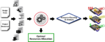
Altair’s Hardware Emulator Resource Optimizer (Hero)
Altair® Hero™ is an end-to-end solution designed specifically for hardware emulation environments, addressing all aspects of emulation flow including design compilation, emulator selection, and software and regression tests. Hero’s vendor-independent architecture and comprehensive policy management features provide organizations with flexibility and control.
Hero supports a variety of hardware-assisted verification platforms, including traditional software-based tools as well as hardware emulators based on custom processors and FPGAs. It is designed to be emulator-agnostic, providing a generic scheduling model that treats boards and modules as “leaf” resources, making it adaptable to most commercially available emulation platforms.
Key features of Hero 2.0 include policy management including FairShare and preemption, soft reservations enabling users to reserve blocks of time on an emulator in advance, visibility to emulator-specific metrics for hardware asset optimization and organizational planning, a rich GUI to simplify monitoring and determine the root cause of failing jobs, and support for emulation and prototyping platforms from multiple vendors.
Hero enables emulator users to benefit from the same kinds of policy-based controls common in software verification environments, such as attaching different priorities to different emulation jobs, applying FairShare policies to manage sharing of emulator resources, and preemption ensuring the resources are available during business hours for interactive ICE activities. Hero also provides granular, real-time visibility to emulator resources, including visibility to runtime host allocations and the boards and modules used across the various emulators.
Summary
As per Altair, Hero is the only scheduler to optimize use of resources across multiple emulators and hardware-assisted verification platforms. Altair has published two whitepapers around Hero to address the topic of optimizing the use of emulation resources. Those involved with running workloads on emulators would find these two whitepapers very informative.
The first whitepaper covers the details of how Hero helps maximize the ROI of customers’ emulator resources. This whitepaper goes into many intricate details as they relate to hardware emulation. For example, it identifies a number of business tangible metrics to track to evaluate the utilization efficiency of emulation resources rather than the simplistic metric of percentage of emulator gates used. The second whitepaper is more like an application notes on how users can apply the features of Hero for their emulation jobs.
For more details, visit the Altair Hero product page.
Also Read:
Measuring Success in Semiconductor Design Optimization: What Metrics Matter?
Load-Managing Verification Hardware Acceleration in the Cloud