Those of you who have been in the industry for a little while will remember that the recipe for reliable electronics in cars (and other vehicles) used to be simple. Stick to old (like 10 years old) and well-proven processes and tweak rather than tear up and restart well-proven designs to the greatest extent possible. Because incrementing from a well-characterized base should ensure that reliability and other KPIs will not drift too far from expectations.
That recipe went out the window when we demanded that our vehicles turn into phones on wheels, offering ADAS, autonomy, advanced infotainment, requiring state of the art processes and architectures. Throwing out the rulebook gets us all the functionality; however, we don’t expect our phones to be ultra-safe or work reliably for 20 years or more. How do we bridge the gap between all the technology goodies we want and our safety and durability expectations?
proteanTecs recently hosted a webinar I rate a must-watch on this and related topics. Packed with information and informed opinion, it measurably increased my understanding of challenges and directions towards bringing high reliability to advanced technologies. More generally it helps build greater understanding of the need for electronics lifetime monitoring and adaptation. Participants were Heinz Wagensonner (Senior SoC designer at Cariad, the automotive software branch of Volkswagen), Jens Rosenbusch (Senior Principal Engineer, SoC safety architecture at Infineon), Robert Jin (Automotive safety architect at NXP), Gal Carmel (Senior VP/GM for automotive at proteanTecs), and moderator Ellen Carey (Chief External Affairs Officer at Circulor).
What Auto Reliability Means Today
One aspect of enhanced reliability is in fail-safe or fail-degraded systems. Real systems can and will fail. Acknowledging this reality, when a system is failing or expected to fail, a redundant system can take over or the system can fall back to reduced functionality, still safe enough to allow the car to limp home or perhaps to the side of the freeway. This reasoning is already well understood, though is expected to be applied more widely in future designs.
Another aspect – the subject of this webinar – recognizes that high reliability cannot be assured in a system which fails to evolve over time. Devices age, use-cases change, the environment changes, and feature capabilities will be upgraded. Few of these changes can be accounted for in the t=0 (product release) system. Systems must become intelligently self-monitoring, responding in part through locally determined adaptation but also through a feedback loop to a central resource which can synthesize broader learning for dissemination back to vehicles.
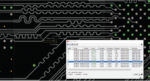
In short, for continued high reliability in these advanced systems, closing the spec for t=0 is only the start. You move to Arizona (hot) and your daily commute doubles. You are now pulling a trailer and have downloaded a software upgrade to your vehicle (now 10 years old) which promises to improve your range (ICE or EV). The “spec” keeps changing yet reliability plus safety must continue to measure up to the highest standards. This demands in-system and in-circuit monitoring through embedded sensors for workload, temperature, voltage, interconnect, and delay monitoring (for example) together with on-board ML-driven intelligence to interpret that data. This should capture not only immediate problems but also anomalous signatures which might indicate the beginning of a future problem. Allowing us to supplement now routine safety mitigations with the beginnings of predictive maintenance.
What constitutes a problem or a suspicious signature depends on mission profiles. One size does not fit all, for example a robotaxi, a city business vehicle, a personal car in the city or in rural use, will have different profiles. An important aspect of profiles will be factors affecting power: voltages and frequencies for example. Lowering power improves thermal reliability of course but will also extend range in an EV, also a positive for reliability.
Profiles can’t be programmed into a product at release, not least because we have no idea (yet) what those profiles should be. The t=0 spec must somehow accommodate the full range of possibilities, which designers accomplish through margins, margins everywhere which is expensive. In use, it will become clear for a certain profile that some margins can be tightened, whereas others perhaps should be loosened. Intelligent systems can learn their way to profile optimization, even better if they can share data with other cars.
From Theory to Practice
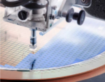
Naturally proteanTecs plays an important part in this solution. During chip design, they build and insert low impact agents, guided by detailed analysis, into the design to assure high coverage data in use. Working in partnership with proteanTecs, NXP have written a paper which became a driver for the ISO/TR:9839 standard on predictive maintenance. This is expected to fold into or alongside the next rev of the ISO 26262 standard.
This method for capturing and utilizing in-use behaviors is a starting point, however all participants agree that the next interesting/challenging step to derive full value is to collaboratively share this data, certainly within a brand, even across brands for common subsystems, say for engine and braking. Complementary value could be found in considering reliability of total system (the car) rather just individual component or subsystems. In both cases there is rich potential for AI to detect signature patterns in this collective data, patterns which perhaps appear only in multi-factor correlations that we would find hard to detect ourselves.
Sharing data is always a tricky topic these days. Since the types of data discussed here is relatively low-level, I would think so privacy concerns may not be as big an issue as brand competitive concerns. All panelists agreed on the need to build an ecosystem together with regulatory bodies to develop and support standards in this area.
There were several other interesting points raised. Will Tier1s disappear as OEMs build their own silicon? (no). How will this approach simplify analysis for field failures? (massively). Can chiplets help with reliability? (Maybe in the next decade after multi-die system reliability has been proven to automotive expectations for temperature, vibration and humidity).
Watch the replay for more detail on all points.