
In our interconnected world, systems ranging from smart cities and autonomous vehicles to industrial control systems and healthcare devices have become everyday components of our lives. This fusion of physical and digital systems has led to a term called cyber-physical system (CPS). Ubiquitous connectivity is exposing the systems to a wide range of cyber-threats and robust security measures are needed to safeguard the systems.
Securing the Chip, the Cloud and the Communications
At the heart of cyber-physical systems are the chips that control various functions. Securing these chips is crucial because compromised hardware can lead to vulnerabilities that are nearly impossible to detect. Cryptography plays a role at this level by ensuring that the communication between different components of a chip is secure and the data is protected. One of the exciting developments in chip-level security is the integration of hardware-based security features that work in tandem with cryptographic protocols. These features can include physically unclonable functions (PUFs), secure enclaves, and tamper-resistant designs. Such measures not only protect data at rest but also help prevent attacks on the chip’s operation. In the context of CPS, secure communication between devices and the cloud is paramount. Whether it’s transmitting data from sensors in an industrial setting or updating the software on an autonomous vehicle, the integrity of this communication is imperative. And, the cloud is where the data from CPS is often processed, stored, and analyzed and is a prime target for cyberattacks. Leveraging cryptography in cloud security protocols is vital to safeguarding the data and services hosted on the cloud. This ensures that even if bad actors gain access to the cloud infrastructure, they won’t be able to decipher sensitive information.
The field of cryptography is quite advanced and time-tested encryption algorithms such as RSA and ECC have been widely-deployed to ensure cyber-security of connected systems. But dedicated hardware support is very important as secure processing and management cannot be accomplished solely with software.
But the onset of quantum computing poses a significant threat to current cryptographic methods.
Post-Quantum Cryptography (PQC)
To counter the quantum threat, researchers are developing post-quantum cryptography, a new generation of cryptographic techniques that are designed to withstand attacks from quantum computers. These cryptographic methods are being designed to be quantum-resistant, ensuring that the confidentiality and integrity of data remain intact in a quantum-powered world. Post-quantum cryptographic algorithms can be employed to secure the communication channels, ensuring that data remains confidential and protected from quantum eavesdropping. Techniques like lattice-based cryptography, code-based cryptography, and hash-based cryptography offer robust security even against quantum adversaries. While PQC is in various stages of standardization currently, what customers need now are solutions that can be easily upgraded to incorporate PQC.
The ease of upgrading CPS to incorporate PQC protection is essential in order to expect rapid adoption of cyber-threat safeguards across a very wide base of systems. This means deploying embedded security systems that are PQC ready. Secure-IC offers solutions that fit this criterion.
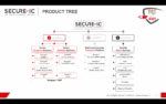
Secure-IC’s Securyzr: Ultimate Solution for Embedded Security
Securyzr delivers state-of-the-art hardware and software security solutions, designed to meet the demands of a wide range of applications, from IoT devices and automotive systems to critical infrastructure and smart cards. With a focus on adaptability, scalability, and efficiency, Securyzr seamlessly integrates into existing systems while ensuring they remain impervious to attacks. Securyzr’s quantum-resistant cryptographic algorithms, ensure data remains safe and confidential even in the era of quantum computing. Its hardware-based Root of Trust, protects against unauthorized access and tampering and its secure boot and firmware update mechanisms prevent malicious code injection. Evolving threats can be handled with ease by employing dynamic security policies that can be updated remotely, ensuring that devices can stay secure throughout their lifecycle. Embedded systems can meet evolving industry-specific security standards and certifications easily.
Secure-IC’s Laboryzr: Unlock the Power of Security Testing
Laboryzr is a comprehensive security testing platform that enables thorough evaluation of the robustness of integrated circuits (ICs), embedded systems, and software applications. With a powerful suite of testing modules and an intuitive user interface, Laboryzr simplifies the complex process of security assessment. Laboryzr provides in-depth security analysis and identifies vulnerabilities and weaknesses in your products, allowing you to address them proactively. By simulating real-world cyberattacks, Secure-IC performs penetration testing to evaluate a system’s resistance to external threats. It performs side-channel analysis to detect potential information leakage through side-channel attacks and allowing to mitigate them, securing sensitive data from unauthorized access. Laboryzr also provides detailed, actionable reports that help you understand the security posture of your systems and make informed decisions to enhance protection.
Secure-IC’s Expertyzr: Elevate Your Expertise in Embedded Security
Expertyzr is a cutting-edge educational platform, crafted to empower professionals, engineers, and security enthusiasts with the expertise needed to navigate the complex landscape of embedded security. With a wealth of resources, hands-on labs, and expert insights, Expertyzr is a gateway to mastering the art of secure embedded systems. The educational platform covers a wide scope from standardization to design principles, evaluation, and certification schemes among many other topics of interest.
Summary
As we continue to embrace cyber-physical systems in our daily lives, the security of these interconnected systems becomes paramount. While quantum computing poses a significant threat to current cryptographic methods, PQC offers a promising solution to protect CPS, from the hardware level in chips to the cloud.
To learn more about solutions for implementing secure CPS systems for the post-quantum era, visit www.secure-ic.com.
Also Read:
How Do You Future-Proof Security?
Points teams should consider about securing embedded systems


